Children's toy on logic elements
In this, if I may say so, article I want to tell about my first project in electrical engineering. I must say that I am far from circuit engineering and radio electronics by the nature of my activities, but my interest in this topic has given me no peace from an early age. For people with experience, the information below may seem too obvious, and a lot of things made by me - the invention of the bicycle. But maybe some noob, like me, will be able to discover something new and interesting. Who cares, I ask under the cat.
It all started with the idea to make a development board for my little daughter. First of all, I wanted to stretch my arms and do something myself. Secondly, I wanted to stretch the brain and come up with something that is not on ordinary boards of this type.
After observing what the child likes to do most in everyday life, it was decided that in addition to the standard handle-latch chains, you need to add buttons for pressing and some device that reflects the response to pressing. Since it should have been displayed something simple, but bright, the choice fell on a red LED matrix 8x8.
Before the creation of the toy, I had been collecting dust for some time on the shelf of the Arduino Uno - I waited until I could come up with something useful besides the system of watering the flowers, which, apart from the pitch boredom itself, was a little less than I didn’t need. I thought that it was her (Arduino) hour, because you need to start somewhere. After reading the manuals for the matrix, I learned that in addition to not simply connecting it to the Arduino (only for it you need 16 pins, which are not in my Arduino), you cannot control all the LEDs at the same time. You can simultaneously shine certain diodes or in one line, or in one column (control of a common cathode, or a common anode). And if you do this consistently and quickly enough, the person stops perceiving the blinking and sees a stable picture. I also found out that for Arduino there are ready-made drivers and libraries that take the pain of managing this process. And the fact of the absence of such a driver at that time predetermined the outcome of the entire project.
While I was all over the process and postponed the choice of the best place to buy a driver, I was struck by an article about the operation of trigger systems. For my brain of the humanities, it became a real discovery, giving an understanding of how memory is arranged at a primitive level. It was then that I wondered if I could do without the Arduino and make my project based on triggers and logic circuits.
So, first you had to decide what to show and how to do it. It was clear that it was necessary to take turns signaling on eight rows of the matrix and for each iteration to feed a parallel signal to specific columns. Well, it gave me an understanding of the three main components — a pulse generator, a clock pulse converter into eight consecutive signals, and a converter that for each of the eight signals will output a certain combination of parallel signals. Everything is not so difficult.
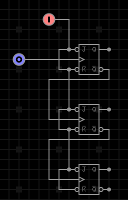
After some thought, a circuit was formed in which a clock signal is converted into a binary code using three successively connected JK-flip-flops, and then using logical circuits into an octal one. Details on this type of trigger can be read at least on Wikipedia. In short, it has two inputs (J and K) and two outputs (Q and Q̄), as well as a synchronization input (CLK). When applying a logical unit to one of the inputs at the next synchronization pulse, the unit will be displayed on the corresponding output and remain on it regardless of whether a synchronizing pulse is applied again and the value on the selected input changes, provided that there is zero on the second input. If you submit the unit to the second input, and the first zero, then at the next synchronization pulse, the value of the first output will change to zero, and the second one to one. But if a unit is applied to both trigger inputs, then with each synchronization pulse, the unit will alternately appear on one of the outputs. And if you take two triggers, apply a clock pulse to the sync input of the first, and to the sync input of the second signal from the output Q̄ of the first, as a result, the output of Q1 will output one every two clock cycles, and Q2 every four. This will result in a two-digit binary counter. And if you add the third trigger in the same way, then at the expense of the third digit you can count up to eight with a binary code - that is necessary.
Next, it was necessary to create a truth table and select a set of logical keys so that the binary code can be turned into eight consecutive signals. If for someone truth tables and boolean operations are something new and unknown, then you can read about them again on Wikipedia here and here .
It would seem that there is half the battle, but in fact, it was not so simple. When I assembled the first part of the scheme for the test on the layout and presented how to implement the second part in the same way, my imagination drew many months (and maybe years - the time to practice a hobby is a little more than an hour after work) of drawing schemes and compiling truth tables. After all, for eight rows of each picture you need to generate a unique combination of columns. And the more pictures there are, the more monstrous the scheme will be. I realized that it would not work to make my plans on logical keys alone. It was necessary to look for something that could simplify the process.
The solution was a memory chip. EEPROM (Electrically Erasable Programmable Read-Only Memory), a programmable memory with the possibility of electrical erasure with parallel input / output, was well suited for my task. Memory has as far as address inputs, which, in essence, are bits of the binary address of memory cells. That is, if the memory has n address inputs, you can program 2 ^ n cells. The number of memory pins is the so-called "word length", or the actual length of a binary string that can be written to each cell. The product of the number of cells by the length of the words determines the amount of memory in bits.
The incoming signal in the form of a binary code was available at the output of JK-flip-flops. It remains to supplement it with bits from the buttons, which should be responsible for the output of different pictures, and it's in the bag.
Again, the lack of experience did not give me an adequate assessment of the complexity of the process. After all, the memory must be programmed, and for this you need a programmer - the device is noticeably expensive in order to purchase it for a one-time toy crafts. Googling showed that theoretically it could be done with the help of Arduino. But for programming, it is necessary to simultaneously send signals to the address inputs of the memory chip and to the pins, which subsequently must reproduce the signal. And still need control signals recording chip. That is, again more than the available pins. Additional googling has opened for me a shift register - a chip that remembers the specified sequence of zeros and ones and displays them on parallel outputs. Often, these chips also work as a buffer and have an output that can consistently reproduce the signals at the input. I.e, If you connect to it the next same register, then you can simultaneously display a twice as large sequence than for one. As you enter a string, the first part of it will go through the first register as a buffer to the second, and the rest will remain in the first register. By adding a third register, you can triple the length of the string, etc. To implement this, it was necessary to write a sketch in an unfamiliar programming language. But having some experience in Python and many examples on the Internet, after a series of trial and error, this task turned out to be quite feasible. Sketch can be taken on By adding a third register, you can triple the length of the string, etc. To implement this, it was necessary to write a sketch in an unfamiliar programming language. But having some experience in Python and many examples on the Internet, after a series of trial and error, this task turned out to be quite feasible. Sketch can be taken on By adding a third register, you can triple the length of the string, etc. To implement this, it was necessary to write a sketch in an unfamiliar programming language. But having some experience in Python and many examples on the Internet, after a series of trial and error, this task turned out to be quite feasible. Sketch can be taken ongithabe .
And here the sketch is written, the microcircuit is connected, running and ... nothing - the memory is not programmed. Some samples, change of parameters of record, and any results. The chip I had was a W27C512-45Z. A careful reading of the manuals showed an unpleasant moment. To write to a specific contact on the chip, you must apply a current of 0.03A with a voltage of 12V. I thought I just bought a not quite suitable chip. But having gone through the counters of local electrical component stores, I made sure that 12V is necessary for everyone. Laboratory power supply I did not have. There are lots of 12V blocks in the house, but they are all pulsed, besides the current is about 1A. Forgive me for experienced engineers for such blasphemy, but in desperation, I decided to try, if a miracle would happen to those blocks that were at hand. Did not happen. The first two passes of the recording yielded nothing
On the Internet, I found references to a certain ST662AB microcircuit — a 5V-12V converter — which, when assembled with the necessary set of capacitors, should produce the necessary current and voltage. In fact, it was not easy to find a microcircuit. As a result, I ordered it from China, also SMD. And what to do from four to six weeks of delivery? Right, learn. Scrolling through the articles on memory programming, I came across the mention of a microchip that can be programmed at 5V. It was about AT28C256. And indeed, in the datasheets to her no mention of 12V was not. Need to take! True, the chip for my needs was a bit redundant, since it allowed me to save 256Kb: 8-bit output for 32K addresses, which, given the busy three address pins for string synchronization signals, left the possibility to encode as many as 4096 images (10 would suffice me). Besides, delivery had to do as much from the UK. But I did not find any other options, and in the end, the memory can be reprogrammed, and when the toy loses its relevance, the chip can be used somewhere else. So after four days I had a memory. Test run of the sketch, and happiness - everything works.
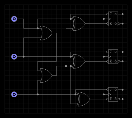
The last thing left is to decide how many buttons there will be, draw 8x8 pictures and realize adding signals from the buttons to the scheme. Having estimated the place on the board, I stopped at five buttons. Considering the worthless demand in comparison with the memory resource, the easiest way was to send a signal from each button directly to a separate input without applying any coding. True, I also had to solve the problem of switching between pictures. You could use the buttons with a latching pressure. But such an implementation was not suitable for use by a one-year-old child, because then, before pressing the next button, it was necessary to press the working one, and it was rather primitive in itself. I wanted to come up with a scheme for non-latching buttons, in which the pressing of each button would be saved, and even canceling the pressing of the previous one. I read about the features of the use of different types of triggers, hoping that some of them can solve this problem on their own, but alas. After sitting a little with a piece of paper and a pencil, I came up with the following scheme (an example for three buttons).
First you need to connect all the buttons to a collector, which at the output will give a unit when you click on any of the buttons. The OR key is suitable for this. Since most key chips have only two inputs, it is necessary to connect the first two buttons to one key, then to connect its output to the first input of the second key, and to its second input - the third button. In this way, you can continue to connect more buttons, adding a new key for each subsequent one. In addition, each button must be connected to a separate XOR key and to J an input of a separate JK-flip-flop. Connect the output of the OR buffer to the second input of the XOR keys, and the output of each XOR key to the K input of the corresponding JK-trigger. Thus, by pressing, for example, button 1, one will be fed to J1, and XOR1 will not work, since one is fed to it from the button, and from the OR buffer. At the output of Q1, the unit will also appear and will be saved. At the same time, XOR2 and XOR3 will work, giving a unit to K2 and K3. And if Q2 or Q3 was previously one, it will change to zero.
Coming up with 8x8 images was also a separate challenge. Too few points to reproduce a recognizable image. But turning on the fantasy, still managed to draw a few, for example such an android.

For pictures, I created truth tables. But since it is necessary to supply a unit to the matrix for the rows, and for the columns it is zero, the table had to be inverted. I wrote the resulting binary code in hexadecimal encoding for more convenient use in the Arduino sketch.
To build the whole scheme, I wanted to order a ready-made board. But from the list of available firms offering layout services for the layout, the cheapest version of double-sided board was offered to me for almost $ 25. I do not know, maybe this is a normal price, but it seemed to me a bit too much. In addition, I have absolutely no experience in designing layouts. And I also find the soldering process very pleasant and soothing. Therefore, I bought a universal fee, a roll of colored wire, the necessary components and sat down for a few evenings at the assembly. Since all components operate on voltages from 5V to 12V. For convenience, I made power from a 9V battery.
How everything works as a result, you can see here , the full scheme is available on github .
As a "heart" of the whole circuit, I used a pulse generator. I was not sure what exactly the frequency of the clock pulse is needed, so I used the finished circuit with the adjustment. I, unfortunately, do not have an oscilloscope, but by comparison of the adjustments and the datasheet of the scheme, it is used somewhere 1KHz. Here the video shows how the frequency changes from low to higher, you can see how the rows of the matrix are drawn.
Thanks for attention.