NES, implementation on FPGA
Good day!
I want to talk about the project of the Nintendo Entertainment System (NES) game console in the implementation on FPGA. In the post-Soviet space, she is known as Dendy.
For those who want to watch the video and nostalgia, please, under the cat.
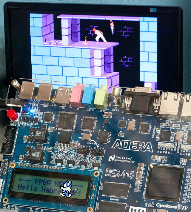
I think most people of my age remember this game console well. She was with me. In the 90s there was not very much money in our family, so I didn’t even have Dandy, but a completely Chinese clone of Subor. I must say that he worked without any complaints, except for the often breaking joysticks, which had to be repaired many times. Of course, after a short period, I could not resist the temptation and dismantled the prefix. It was made on two printed circuit boards, one - an RF modulator and a power supply on the LM7805, installed without a heatsink, it was very hot, and the second processor board, which, unfortunately, was made on a single chip - a drop. As far as I remember, there was nothing more than quartz, a pair of capacitors and a cartridge connector on it. In those days, it was very difficult to find any information, and I did not even know which processor Dandy was running on. Only once I saw NES in a "discrete" implementation with a neighbor - a radio amateur.
A little over six months ago, I ordered an eBay STM32 debug board and saw relatively inexpensive Altera Cyclone II FPGAs, without thinking twice, I ordered it. In general, judging by the forums and opinions of familiar electronic engineers, the FPGA theme is still shrouded in a halo of inaccessibility and the complexity of working with it. I, too, at one time was “seduced” by this error and did not pay due attention to the FPGA topic, as it turned out, completely in vain. I fell in love with FPGA at first sight! Inaccessible for an ordinary amateur radio enthusiast who was engaged in microcontrollers, things suddenly became a reality. For example, full-fledged work with SDRAM, connecting a laptop matrix with the LVDS interface (and the frequencies there are simply killer). My appetites grew, and I bought myself an Altera DE2-115 board, which is used for the NES project. Now I am very sorry that I did not deal with the topic of FPGAs 10 years ago, do not repeat my mistakes, FPGAs are fun and not at all difficult!
Having blinked an LED (by the way, unlike the same STM32, where you need to configure a bunch of peripherals for this, it’s just obscene on FPGA), I decided to do something more serious with a monitor and playing with sound.
What is all this for? As they say, Just for fun. Of course, someone may say that this is already a very ancient platform and there is no particular reason to recreate it on the FPGA, but for me personally it was very pleasant to engage in this project and see the final result. This, if I may say so, how to accidentally find and restore a toy from my childhood, which is associated with fond memories.
In addition, according to the sensations at work, the hardware implementation is significantly different from software simulators. This is partly, of course, the psychological effect, but NES on the FPGA more accurately “keeps” the timings, there are no subtle delays and video artifacts, which in software implementation are caused by attempts to optimize the GPU operation algorithm, which is rather complicated.
In Russian on the network you can find a description of the NES architecture, for example, here .
In principle, the description is pretty good, but you cannot create a working emulator using it, since PPU registers are very superficially described in that article - very important points are omitted.
In this article, I will not describe in detail the architecture and each control register, but I will try to point out possible problems in the implementation of emulators and describe the solutions that I applied in my project. Here is an
electrical diagram of the Nintendo Famicom:

Image from nesdev.com
The core of the A203 (U6) processor is based on the eight-bit microprocessor MOS Technology 6502. On one chip with 6502 is a DMA controller and an audio processor.
On the chip 74LS139 (U3), a CPU address decoder is implemented. The address bus is 16-bit, so the processor can address up to 64 KB. The address space is distributed as follows.

Graphics processor (PPU) 2C02 - U5 chip. To save PPU pins, the lower 8 bits of the address bus are multiplexed with the data bus, so it spends two clock cycles on memory access. For address demultiplexing, the U2 chip is used - register-latch 74LS373 (our analogue of IR22).
To store one video page, 1 KB of memory is required (the background image is composed of blocks (tiles) of 8x8 pixels, and 30 rows of 32 tiles are placed on the screen). The PPU architecture provides for the use of 4 video pages, but only 2KB of video memory (U4 chip) is installed on the NES itself, and the missing 2KB, if necessary, use all 4 pages should be located on the cartridge (page reflection and PPU address space will be discussed below). Honestly, for me, as an engineer, it looks a little wild. It is clear that during the development of the set-top box, such measures were taken for marketing reasons and the cost of the set-top box at the cost of increasing the cost of the cartridge. I don’t know how much 4 KB SRAM cost at that time, but perhaps because of this there are not many games using 4 pages.
The master oscillator is made on transistors Q2, Q3 and generates a frequency of 21.47727 MHz for the NTSC version and 26.6017 MHz for PAL. The CPU core operates at a frequency of about 1.79 MHz, and the PPU pixel frequency is three times higher than the CPU frequency and approximately equal to 5.37 MHz. A relatively high frequency of the generator - 24.47727 MHz is required for encoding color information in a composite video signal and generating a “flash” of the color subcarrier.
Initially, I wanted to find the original NES cartridges and use them, but I did not succeed and this is good, because I had to emulate the cartridge. In the simplest version, a cartridge is just two ROM chips - CPU program memory (PRG ROM) and PPU character generator memory (CHR ROM), in this case the maximum amount of PRG ROM is 32 KB, and CHR ROM is 8 KB. So you can run simple games like Super Mario Bros. 1, Lode Runner, Popeye, etc. Of course, 32 KB is extremely small for a more or less serious game, therefore special solutions (mappers) are used to switch memory banks, which allows expanding the available volume to several megabytes. There are a lot of options for the mappers, as on the discrete logic of the 74 series, for example, the UxROM mapper is built on the counter 74HC161, which is used as a latch and 74HC32 - 4 OR elements, as well as specialized ASIC solutions, for example MMC3. Now the project implements only these two mappers. MMC3 was not chosen by chance, since it was on it that the bulk of everyone’s favorite games were released.
The average cartridge size is about 256 KB, cartridges with a volume of more than 1 MB are very rare. The DE2-115 has 2 MB of SRAM (1M x 16) and 128 MB of SDRAM. I decided that640KB is enough for everyone, 2MB for a cartridge is more than enough and allocated 1 MB for PRG ROM and 1 MB for CHR ROM. The address space is common, in the high byte of the word PRG data is stored, and in the low byte - CHR. Images are downloaded from an SD card from iNES files. For servicing FAT and downloading files, I used the Nios II processor (in terms of NES itself, everything is implemented in hardware, Nios is not used).
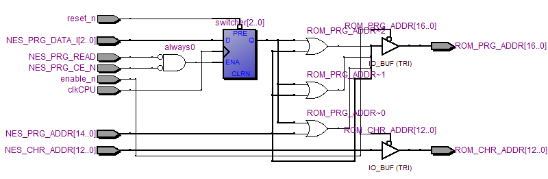
The diagram shows the cartridge emulation unit:

The unit is connected to the Nios II processor with a 4-bit address bus and an 8-bit data bus. The block controller has 7 control registers with which you can control the state of NES - pause, perform a hardware reset, set options for the reflection of video pages, type of mapper, resolution of address buses PRG and CHR ROM. To download the image, there are commands to select the boot area (CHR or PRG), reset the address. After the next byte is written, the address is automatically incremented.
Since the address bus is common for PPU and CPU, the multiplexer unit operates at an increased frequency, in my case it is 32.22 MHz - 6 times higher than the PPU frequency. Further, separate address buses go to the block of mappers, where MMC3 and UxROM are implemented, and the choice of the active mapper sets the state of the control register. If necessary, adding support for any other mapper is very easy.
For example, the UxROM implementation looks like this:
In the original NES, from the hardware point of view, nothing prevents the cartridge from installing the RAM instead of the character generator ROM and initializing it during the program execution, writing through the PPU registers. Such cartridges and games exist, for example, Contra, Castlevania and many other games on UxROM. This approach has its advantages, for example, part of the character generator icons can be synthesized programmatically, you can also store the contents of the character generator in a compressed form and decompress in CHR RAM, this will save a lot of space on the cartridge.
Since I already use RAM to store CHR, this function turned out to be my default.
A USB joystick is used as an input device. USB maintenance is also carried out by the Nios II processor: The
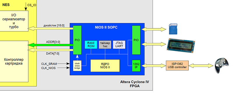
state of all the joystick buttons is packed into a word and enters the serializer block via a parallel bus. The NES processor, recording at address 0x4016, generates a strobe pulse, and the status byte (8 buttons) is loaded into the shift register. Further, when accessing 0x4016 (for the first joystick) and 0x4017 (for the second), the state of the next button is shifted and read. The “Turbo” buttons in the original NES are implemented in the joystick itself and simulate the frequent pressing of the A / B buttons, that is, in fact, the NES does not distinguish which button is pressed, “Turbo A” or “A”. In the project, this function is performed in the serializer block, the frequency is about 20 Hz.
Functionally, PPU can be divided into a background rendering unit and a sprite rendering unit.
If we talk about software emulators, I want to note that although the rendering algorithm itself is simple, but due to the fact that the CPU and PPU work synchronously, creating the correct software emulator is quite a difficult task. More precisely, then implementing a PPU software emulator forehead is quite simple, but such an implementation will consume a lot of resources and will not work optimally. I think that any programmer will be the first to think that if there is an array of tiles on the screen and there is a character generator, then you can draw the entire frame, or at least part of it. Of course, you can draw, but here the problems with the synchronous operation of PPU and CPU will begin. The thing is that to create graphic effects, the CPU can change the PPU control registers directly in the process of rendering the frame and can switch the character generator memory bank, more than once during the frame. Such actions are implemented scrolling the screen with a gap, both vertical and horizontal, fixed areas, the output of all kinds of static information. Therefore, these points must be taken into account, up to the number of cycles for which each CPU command is executed, in order to know exactly at what point in time the CPU performs actions on the PPU control registers.
Due to such features, some software emulators sin with visual artifacts in games, especially those that non-standard use the capabilities of PPU.
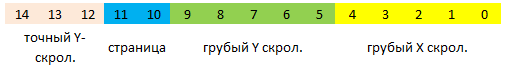
The PPU address space is distributed as follows:
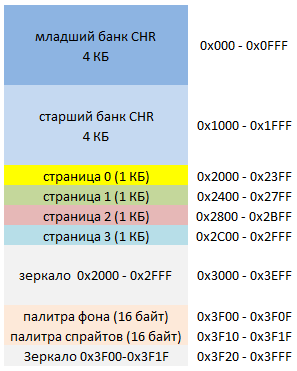
Video pages are arranged in such a way that, for example, with horizontal or vertical scrolling, the screen will show the contents of two pages at once, and with a diagonal - four. The location of the pages and the coordinates are shown in the figure:

As I wrote above, on the NES itself there is 2 KB of RAM for the page memory. Therefore, if a missing memory is not installed on the cartridge, page reflection is applied. Vertical, when the second page reflects zero, and the third - the first, and horizontal - the first page reflects zero, the third - the second.
There is no point in saving 2 KB in a FPGA project, so all 4 KB are allocated for video memory. Hardware reflection is very simple: in the case of vertical reflection at the address bus, the RAM is torn off from the PPU and the 11th bit line is connected to zero, and in the case of the vertical, the 11th and 10th bits are interchanged, and the oldest line is also connected to zero:
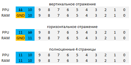
Some mappers can dynamically change page reflection options by switching address bus lines. An example is the game Super Mario Bros. 2, where at the very beginning of the game when falling, horizontal reflection is used, and then switching to vertical.
For interaction with PPU 8 registers are used (meaning the address space of the CPU).
This register monitors the status of the PPU, for example, sets the size of sprites (8x8 or 8x16), the video memory page, and the permission to generate an NMI interrupt.
Register sets the permission to draw sprites and background. Also, it can be used to prohibit rendering at all, and then the CPU will be able to access PPU memory areas at any time, this is used by games during initial initialization of pages when changing the game environment and filling in CHR RAM if RAM was used instead of ROM. Without prohibition, access to the PPU memory is possible only in the VBLANK period, when the PPU does not access it.
This register contains the PPU status flags. This is the fact that the first opaque pixel of the zero sprite began to be drawn, the beginning of the VBLANK period and the flag indicating that more than 8 sprites fall on the current line.
Specifies the address for subsequent manipulation of the sprite memory (Object Attribute Memory - OAM).
Read and write OAM data. After the operation, an auto-increment of the address value occurs. Typically, games do not write to OAM in this way, but use DMA.
Scrolling register. In the first write operation to the register, the value of horizontal scrolling is set, in the second - vertical.
Specifies the address for the subsequent memory operation of video pages. In the first operation, the highest part of the address is specified, in the second - the youngest.
Reading and writing data from the video page memory. After the operation, the address value is automatically incremented by 1 (next column) or 32 (next line), it depends on the state of bit 2 of register 0x2000.
Duplicate registers use a common trigger, so you cannot, for example, write once to 0x2005, then to 0x2006, and then return to 0x2005 again. More precisely, you can, but you need to understand while doing this. If the trigger state is unknown, you can read register 0x2002, and the trigger is reset.
It sounds simple! But there is an extremely important feature that is not indicated in the above-mentioned Russian-language description.
The fact is that the listed registers, so to speak, are not completely independent.
There are two 15-bit registers:
vVRAM- current video memory address (hereinafter simply “v”);
tVRAM - temporary address (hereinafter simply “t”);
and 3-bit register of "exact" scrolling on X (fine X scroll). Sets scrolling (0..7) within 1 tile.
Addresses v and t are formed as follows:
Thus, setting a page by writing to register 0x2000 changes bits 11,10 of register t. Writing to register 0x2005 sets the value of bits 4: 0 and 9: 5/14: 12 of register t and the value of "exact" scrolling in X. But writing to register 0x2006 can ruin everything, since in this way you can change the value of all bits at once register t, and in the second write operation, v = t is copied.
In the process of drawing a line, PPU increases the values of coarse scrolling by X in the register v and accordingly changes the address of the video page when the coarse scrolling value is overflowed. At the end of the visible line (pixels 256-257), the PPU increases the Y value and copies the components related to horizontal scrolling (v [4: 0] = t [4: 0] and v [10] = t [10]). Before starting a new frame (pre-render), the components of the vertical scrolling are copied (v [9: 5] = t [9: 5], v [14:12] = t [14:12], v [11] = t [ eleven]). And it all starts again.
Now it’s clear how, by changing the values of the PPU registers, you can get various background tear effects.
The color of each pixel is selected from the palette. There are separate palettes for background and sprites. A palette is a 16-byte memory area. The zero element of the background palette sets the color of the canvas. When rendering a background pixel, a 4-bit address is generated that points to a color element in the palette. The two most significant bits of the address are the value of the attribute of the tile group, and the two least significant bits are set by the image from the character generator. By changing the attributes of a group, you can change the color of tiles using the same element of the character generator.
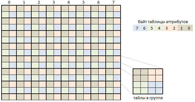
The first 960 bytes of the video page (name table) specify the addresses of the tiles from the CHR character generator located on the page. Each of the remaining 64 bytes of the attribute page sets an attribute to a group of 16 tiles (32x32 pixel area).
16 bytes are used to store the image of one icon in the memory of the character generator. Each pixel, as mentioned above, is encoded in two bits. The first 8 bytes refer to the low-order bit of the pixel, and the next 8 bytes to the high-order bit. That is, a pair of bytes 0 + 8, 1 + 9, etc. line icons set.
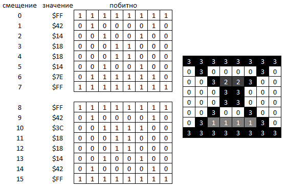
The colors in the example are selected conditionally. Elements that are equal to zero are transparent and the attribute value does not affect them.
Group attributes are set as follows:
One pixel must be drawn in one clock cycle of the PPU. You need to understand that on the original NES, for 2 cycles of PPU we can get only 1 value from memory. Therefore, before the beginning of the line at the end of the HBLANK period, data is sampled for the first two tiles of the new line.
The data necessary for the output of the tile line is sampled in 8 cycles of PPU. First, from the video memory, we get the tile address in the character generator (2 measures), then the group attribute value (2 measures), then the low byte of the tile line from the character generator (2 measures), and, finally, the highest byte of the tile (also 2 measures). And it all starts again.
Since I do not multiplex the address bus with the data bus, in my project I can receive data on each PPU clock.
In the section describing the PPU registers, the area of sprite memory was mentioned - Object Attribute Memory (OAM). Its size is 256 bytes, it is located on a PPU chip in a separate address space, which means that simultaneous and independent of, for example, VRAM and CHR ROM access to this area is possible.
4 bytes are allocated for each sprite in OAM - therefore, no more than 64 sprites can be displayed on the screen at a time.
Images of sprites are also stored in the character generator (CHR ROM).
Each sprite on the screen is described by its position on the screen in X and Y, the address of the icon in the character generator, the attribute (the same as the group attribute when rendering the background), horizontal and vertical reflection flags of the sprite (you can use halves of one icon to display symmetrical objects generator) and the flag of priority.
Sprites can be 8x8 and 8x16 pixels in size.
Sprite image formation is no different from background image formation. However, the hardware implementation again has its own peculiarities.
At the same time as the line is drawn, a search is made for sprites that will be visible (fall) to the next line (in range evaluation). There is a secondary OAM in the PPU that can store information about 8 sprites. If during the search it turns out that there are more than 8 sprites on the next line, then the extra sprites are ignored and a flag is raised in the PPU register 0x2002 to signal this.
Since the CHR ROM bus is busy during line drawing, the data from the symbol generator about the pixel color of these 8 sprites is sampled in the HBLANK period.
NES forms a picture with a resolution of 256x240 pixels. To display the image, I use the standard resolution of VGA 640x480. PPU renders the image into a frame buffer. Data from the frame buffer enters the block in which the resolution is doubled (upscaler). In the future I want to implement hq2x. Before applying data to the video DAC, the color is converted to RGB.
To quickly fill in OAM, the NES processor can use the DMA controller. The DMA controller is implemented very simply. Before starting the copy operation, the CPU must set the OAM start address (register 0x2003), or rather reset it to 0. Then the CPU writes to the address 0x4014 the value of the start address (0x ?? 00) in the address space of the CPU. The DMA controller stops the CPU and starts copying 256 bytes from the area 0x ?? 00 - 0x ?? FF (where ?? is the value specified by the CPU) to the PPU register 0x2004. The PPU increments the OAM address by one for each write operation. At the end of the procedure, the DMA returns control to the CPU.
The final pixel color value is formed as follows:

It is quite possible and often happens that more than one sprite is in the same area.
In this case, the priority of the output to the screen is affected by two factors - this is the value of the sprite address in OAM and the priority flag (0 - foreground, 1 - background). For example, a sprite in which the priority flag indicates that it belongs to the background, but the value of the address in OAM is less than that of the foreground sprite, then the background sprite can close the front sprite, which will lead to the output of the background pixel, but only if it is not transparent.
When rendering the first opaque pixel of the sprite with address 0 (the background at this point should also be opaque), a flag is raised in register 0x2002 indicating that the Sprite 0 hit event has occurred. An example of the application of this flag is the Super Mario Bros. 1, in it it is used to break the screen and separate static information about points and time from the playing area. The coin image serves as the background, and its shadow as the zero sprite. The CPU periodically checks the value of the flag, and when an event occurs, the output of the playing field begins.

Mapper MMC3 includes a line counter, the value of which decreases when the next PPU line is displayed. Upon reaching zero, the counter is reloaded with a value that can be set by pre-writing to the corresponding register of the mapper and, if the enable flag is set, a CPU interrupt occurs. The counter clocking line is organized in a rather original way - it is connected to the address line A12 of the GPU. For storing background tiles, the lower bank is usually used (region 0x000 - 0x0FFF), and for sprites, the senior bank (region 0x1000 - 0x1FFF). When drawing a visible line, PPU refers to one bank, and when fetching sprite image data in HBLANK, the period refers to another. Therefore, the frequency on line A12 will correspond to the line output frequency.
You can look at examples on video.
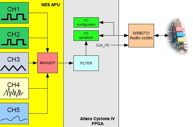
The NES audio processor is on the same chip as the CPU. Functionally, the APU is a set of control registers, a frame counter and 5 blocks of audio channels.
From a hardware point of view, the APU is a bunch of counters, there are no pitfalls there, so the description will be brief.
The frame counter generates clock pulses with a frequency of approximately 240 Hz, 120 Hz for APUs, as well as IRQ interrupt for the CPU. Interrupt generation can be turned off by setting APU registers. The concept of “frames” should not be confused, in this case it has nothing to do with PPU.
By the way, an unpleasant incident occurred during development, the APU frame counter was already implemented and I messed up the interrupt enable flag (it turned out to be inverted), so the interrupt was generated with a frequency of about 60 Hz. Outwardly, this manifested itself very unexpectedly - in the game “Prince of Persia”, on the left side of the screen, the doorway with a grill was not displayed, and this was the only graphic artifact. I broke my head until I found the real reason. And I thought, of course, on PPU - I checked the code a hundred times, looking in ModelSim. It was unpleasant!
The APU has five channels:
Two rectangular channels, as the name implies, they form a square wave, one triangular channel, one noise channel and a delta modulation channel (DMC).
Rectangular channels can form a signal with variable duty cycle (4 gradations) and a period, with the ability to set the duration, and also have sweep and envelope blocks. The sweep block can change (sequentially increase or decrease) the signal period in time, and the envelope block (envelope) - reduce the signal amplitude in time with the possibility of looping, the envelope shape in this case is sawtooth.
The triangular channel generates a triangular signal with a variable frequency and duration, however, it does not have the ability to adjust the volume.
The noise channel generates a pseudo-random signal with a variable duration. As well as a rectangular channel, the noise channel has an envelope control unit.
The channel of delta modulation in the project has not yet been implemented.
Mixing of channels is carried out in a tabular way, so as not to use “heavy” operations in terms of consumption of LE.
After mixing, the signal enters the domain synchronization block and the filter, after which it goes to the WM8731 audio codec via the I2S serializer block.
When implementing the project, I used the Verilog 2001 hardware description language.
Anticipating questions regarding the source code, I can say that, since this is my first big FPGA project, I probably implemented many things in a very inefficient way. In addition, this is the very first version, the code needs to be optimized and cleaned up, because I rewrote many blocks several times. Therefore, I would not want to provide it in this form. If I find the time, get together and put the code in order, then maybe it will be posted under the GNU GPL license.
Thanks for attention!
I want to talk about the project of the Nintendo Entertainment System (NES) game console in the implementation on FPGA. In the post-Soviet space, she is known as Dendy.
For those who want to watch the video and nostalgia, please, under the cat.
I think most people of my age remember this game console well. She was with me. In the 90s there was not very much money in our family, so I didn’t even have Dandy, but a completely Chinese clone of Subor. I must say that he worked without any complaints, except for the often breaking joysticks, which had to be repaired many times. Of course, after a short period, I could not resist the temptation and dismantled the prefix. It was made on two printed circuit boards, one - an RF modulator and a power supply on the LM7805, installed without a heatsink, it was very hot, and the second processor board, which, unfortunately, was made on a single chip - a drop. As far as I remember, there was nothing more than quartz, a pair of capacitors and a cartridge connector on it. In those days, it was very difficult to find any information, and I did not even know which processor Dandy was running on. Only once I saw NES in a "discrete" implementation with a neighbor - a radio amateur.
A little over six months ago, I ordered an eBay STM32 debug board and saw relatively inexpensive Altera Cyclone II FPGAs, without thinking twice, I ordered it. In general, judging by the forums and opinions of familiar electronic engineers, the FPGA theme is still shrouded in a halo of inaccessibility and the complexity of working with it. I, too, at one time was “seduced” by this error and did not pay due attention to the FPGA topic, as it turned out, completely in vain. I fell in love with FPGA at first sight! Inaccessible for an ordinary amateur radio enthusiast who was engaged in microcontrollers, things suddenly became a reality. For example, full-fledged work with SDRAM, connecting a laptop matrix with the LVDS interface (and the frequencies there are simply killer). My appetites grew, and I bought myself an Altera DE2-115 board, which is used for the NES project. Now I am very sorry that I did not deal with the topic of FPGAs 10 years ago, do not repeat my mistakes, FPGAs are fun and not at all difficult!
Having blinked an LED (by the way, unlike the same STM32, where you need to configure a bunch of peripherals for this, it’s just obscene on FPGA), I decided to do something more serious with a monitor and playing with sound.
What is all this for? As they say, Just for fun. Of course, someone may say that this is already a very ancient platform and there is no particular reason to recreate it on the FPGA, but for me personally it was very pleasant to engage in this project and see the final result. This, if I may say so, how to accidentally find and restore a toy from my childhood, which is associated with fond memories.
In addition, according to the sensations at work, the hardware implementation is significantly different from software simulators. This is partly, of course, the psychological effect, but NES on the FPGA more accurately “keeps” the timings, there are no subtle delays and video artifacts, which in software implementation are caused by attempts to optimize the GPU operation algorithm, which is rather complicated.
In Russian on the network you can find a description of the NES architecture, for example, here .
In principle, the description is pretty good, but you cannot create a working emulator using it, since PPU registers are very superficially described in that article - very important points are omitted.
In this article, I will not describe in detail the architecture and each control register, but I will try to point out possible problems in the implementation of emulators and describe the solutions that I applied in my project. Here is an
electrical diagram of the Nintendo Famicom:
Image from nesdev.com
The core of the A203 (U6) processor is based on the eight-bit microprocessor MOS Technology 6502. On one chip with 6502 is a DMA controller and an audio processor.
On the chip 74LS139 (U3), a CPU address decoder is implemented. The address bus is 16-bit, so the processor can address up to 64 KB. The address space is distributed as follows.
Graphics processor (PPU) 2C02 - U5 chip. To save PPU pins, the lower 8 bits of the address bus are multiplexed with the data bus, so it spends two clock cycles on memory access. For address demultiplexing, the U2 chip is used - register-latch 74LS373 (our analogue of IR22).
To store one video page, 1 KB of memory is required (the background image is composed of blocks (tiles) of 8x8 pixels, and 30 rows of 32 tiles are placed on the screen). The PPU architecture provides for the use of 4 video pages, but only 2KB of video memory (U4 chip) is installed on the NES itself, and the missing 2KB, if necessary, use all 4 pages should be located on the cartridge (page reflection and PPU address space will be discussed below). Honestly, for me, as an engineer, it looks a little wild. It is clear that during the development of the set-top box, such measures were taken for marketing reasons and the cost of the set-top box at the cost of increasing the cost of the cartridge. I don’t know how much 4 KB SRAM cost at that time, but perhaps because of this there are not many games using 4 pages.
The master oscillator is made on transistors Q2, Q3 and generates a frequency of 21.47727 MHz for the NTSC version and 26.6017 MHz for PAL. The CPU core operates at a frequency of about 1.79 MHz, and the PPU pixel frequency is three times higher than the CPU frequency and approximately equal to 5.37 MHz. A relatively high frequency of the generator - 24.47727 MHz is required for encoding color information in a composite video signal and generating a “flash” of the color subcarrier.
Cartridge emulation
Initially, I wanted to find the original NES cartridges and use them, but I did not succeed and this is good, because I had to emulate the cartridge. In the simplest version, a cartridge is just two ROM chips - CPU program memory (PRG ROM) and PPU character generator memory (CHR ROM), in this case the maximum amount of PRG ROM is 32 KB, and CHR ROM is 8 KB. So you can run simple games like Super Mario Bros. 1, Lode Runner, Popeye, etc. Of course, 32 KB is extremely small for a more or less serious game, therefore special solutions (mappers) are used to switch memory banks, which allows expanding the available volume to several megabytes. There are a lot of options for the mappers, as on the discrete logic of the 74 series, for example, the UxROM mapper is built on the counter 74HC161, which is used as a latch and 74HC32 - 4 OR elements, as well as specialized ASIC solutions, for example MMC3. Now the project implements only these two mappers. MMC3 was not chosen by chance, since it was on it that the bulk of everyone’s favorite games were released.
The average cartridge size is about 256 KB, cartridges with a volume of more than 1 MB are very rare. The DE2-115 has 2 MB of SRAM (1M x 16) and 128 MB of SDRAM. I decided that
The diagram shows the cartridge emulation unit:
The unit is connected to the Nios II processor with a 4-bit address bus and an 8-bit data bus. The block controller has 7 control registers with which you can control the state of NES - pause, perform a hardware reset, set options for the reflection of video pages, type of mapper, resolution of address buses PRG and CHR ROM. To download the image, there are commands to select the boot area (CHR or PRG), reset the address. After the next byte is written, the address is automatically incremented.
Since the address bus is common for PPU and CPU, the multiplexer unit operates at an increased frequency, in my case it is 32.22 MHz - 6 times higher than the PPU frequency. Further, separate address buses go to the block of mappers, where MMC3 and UxROM are implemented, and the choice of the active mapper sets the state of the control register. If necessary, adding support for any other mapper is very easy.
For example, the UxROM implementation looks like this:
In the original NES, from the hardware point of view, nothing prevents the cartridge from installing the RAM instead of the character generator ROM and initializing it during the program execution, writing through the PPU registers. Such cartridges and games exist, for example, Contra, Castlevania and many other games on UxROM. This approach has its advantages, for example, part of the character generator icons can be synthesized programmatically, you can also store the contents of the character generator in a compressed form and decompress in CHR RAM, this will save a lot of space on the cartridge.
Since I already use RAM to store CHR, this function turned out to be my default.
Enter
A USB joystick is used as an input device. USB maintenance is also carried out by the Nios II processor: The
state of all the joystick buttons is packed into a word and enters the serializer block via a parallel bus. The NES processor, recording at address 0x4016, generates a strobe pulse, and the status byte (8 buttons) is loaded into the shift register. Further, when accessing 0x4016 (for the first joystick) and 0x4017 (for the second), the state of the next button is shifted and read. The “Turbo” buttons in the original NES are implemented in the joystick itself and simulate the frequent pressing of the A / B buttons, that is, in fact, the NES does not distinguish which button is pressed, “Turbo A” or “A”. In the project, this function is performed in the serializer block, the frequency is about 20 Hz.
PPU
Functionally, PPU can be divided into a background rendering unit and a sprite rendering unit.
If we talk about software emulators, I want to note that although the rendering algorithm itself is simple, but due to the fact that the CPU and PPU work synchronously, creating the correct software emulator is quite a difficult task. More precisely, then implementing a PPU software emulator forehead is quite simple, but such an implementation will consume a lot of resources and will not work optimally. I think that any programmer will be the first to think that if there is an array of tiles on the screen and there is a character generator, then you can draw the entire frame, or at least part of it. Of course, you can draw, but here the problems with the synchronous operation of PPU and CPU will begin. The thing is that to create graphic effects, the CPU can change the PPU control registers directly in the process of rendering the frame and can switch the character generator memory bank, more than once during the frame. Such actions are implemented scrolling the screen with a gap, both vertical and horizontal, fixed areas, the output of all kinds of static information. Therefore, these points must be taken into account, up to the number of cycles for which each CPU command is executed, in order to know exactly at what point in time the CPU performs actions on the PPU control registers.
Due to such features, some software emulators sin with visual artifacts in games, especially those that non-standard use the capabilities of PPU.
The PPU address space is distributed as follows:
Video pages are arranged in such a way that, for example, with horizontal or vertical scrolling, the screen will show the contents of two pages at once, and with a diagonal - four. The location of the pages and the coordinates are shown in the figure:
As I wrote above, on the NES itself there is 2 KB of RAM for the page memory. Therefore, if a missing memory is not installed on the cartridge, page reflection is applied. Vertical, when the second page reflects zero, and the third - the first, and horizontal - the first page reflects zero, the third - the second.
There is no point in saving 2 KB in a FPGA project, so all 4 KB are allocated for video memory. Hardware reflection is very simple: in the case of vertical reflection at the address bus, the RAM is torn off from the PPU and the 11th bit line is connected to zero, and in the case of the vertical, the 11th and 10th bits are interchanged, and the oldest line is also connected to zero:
Some mappers can dynamically change page reflection options by switching address bus lines. An example is the game Super Mario Bros. 2, where at the very beginning of the game when falling, horizontal reflection is used, and then switching to vertical.
PPU registers
For interaction with PPU 8 registers are used (meaning the address space of the CPU).
Register 0x2000 (write only)
This register monitors the status of the PPU, for example, sets the size of sprites (8x8 or 8x16), the video memory page, and the permission to generate an NMI interrupt.
Register 0x2001 (write only)
Register sets the permission to draw sprites and background. Also, it can be used to prohibit rendering at all, and then the CPU will be able to access PPU memory areas at any time, this is used by games during initial initialization of pages when changing the game environment and filling in CHR RAM if RAM was used instead of ROM. Without prohibition, access to the PPU memory is possible only in the VBLANK period, when the PPU does not access it.
Register 0x2002 (read only)
This register contains the PPU status flags. This is the fact that the first opaque pixel of the zero sprite began to be drawn, the beginning of the VBLANK period and the flag indicating that more than 8 sprites fall on the current line.
Register 0x2003 (write only)
Specifies the address for subsequent manipulation of the sprite memory (Object Attribute Memory - OAM).
Register 0x2004 (write / read)
Read and write OAM data. After the operation, an auto-increment of the address value occurs. Typically, games do not write to OAM in this way, but use DMA.
Register 0x2005 (write only)
Scrolling register. In the first write operation to the register, the value of horizontal scrolling is set, in the second - vertical.
Register 0x2006 (write only)
Specifies the address for the subsequent memory operation of video pages. In the first operation, the highest part of the address is specified, in the second - the youngest.
Register 0x2007 (write / read)
Reading and writing data from the video page memory. After the operation, the address value is automatically incremented by 1 (next column) or 32 (next line), it depends on the state of bit 2 of register 0x2000.
Duplicate registers use a common trigger, so you cannot, for example, write once to 0x2005, then to 0x2006, and then return to 0x2005 again. More precisely, you can, but you need to understand while doing this. If the trigger state is unknown, you can read register 0x2002, and the trigger is reset.
It sounds simple! But there is an extremely important feature that is not indicated in the above-mentioned Russian-language description.
The fact is that the listed registers, so to speak, are not completely independent.
There are two 15-bit registers:
vVRAM- current video memory address (hereinafter simply “v”);
tVRAM - temporary address (hereinafter simply “t”);
and 3-bit register of "exact" scrolling on X (fine X scroll). Sets scrolling (0..7) within 1 tile.
Addresses v and t are formed as follows:
Thus, setting a page by writing to register 0x2000 changes bits 11,10 of register t. Writing to register 0x2005 sets the value of bits 4: 0 and 9: 5/14: 12 of register t and the value of "exact" scrolling in X. But writing to register 0x2006 can ruin everything, since in this way you can change the value of all bits at once register t, and in the second write operation, v = t is copied.
In the process of drawing a line, PPU increases the values of coarse scrolling by X in the register v and accordingly changes the address of the video page when the coarse scrolling value is overflowed. At the end of the visible line (pixels 256-257), the PPU increases the Y value and copies the components related to horizontal scrolling (v [4: 0] = t [4: 0] and v [10] = t [10]). Before starting a new frame (pre-render), the components of the vertical scrolling are copied (v [9: 5] = t [9: 5], v [14:12] = t [14:12], v [11] = t [ eleven]). And it all starts again.
Now it’s clear how, by changing the values of the PPU registers, you can get various background tear effects.
A bit about image formation
The color of each pixel is selected from the palette. There are separate palettes for background and sprites. A palette is a 16-byte memory area. The zero element of the background palette sets the color of the canvas. When rendering a background pixel, a 4-bit address is generated that points to a color element in the palette. The two most significant bits of the address are the value of the attribute of the tile group, and the two least significant bits are set by the image from the character generator. By changing the attributes of a group, you can change the color of tiles using the same element of the character generator.
The first 960 bytes of the video page (name table) specify the addresses of the tiles from the CHR character generator located on the page. Each of the remaining 64 bytes of the attribute page sets an attribute to a group of 16 tiles (32x32 pixel area).
16 bytes are used to store the image of one icon in the memory of the character generator. Each pixel, as mentioned above, is encoded in two bits. The first 8 bytes refer to the low-order bit of the pixel, and the next 8 bytes to the high-order bit. That is, a pair of bytes 0 + 8, 1 + 9, etc. line icons set.
The colors in the example are selected conditionally. Elements that are equal to zero are transparent and the attribute value does not affect them.
Group attributes are set as follows:
One pixel must be drawn in one clock cycle of the PPU. You need to understand that on the original NES, for 2 cycles of PPU we can get only 1 value from memory. Therefore, before the beginning of the line at the end of the HBLANK period, data is sampled for the first two tiles of the new line.
The data necessary for the output of the tile line is sampled in 8 cycles of PPU. First, from the video memory, we get the tile address in the character generator (2 measures), then the group attribute value (2 measures), then the low byte of the tile line from the character generator (2 measures), and, finally, the highest byte of the tile (also 2 measures). And it all starts again.
Since I do not multiplex the address bus with the data bus, in my project I can receive data on each PPU clock.
Sprites
In the section describing the PPU registers, the area of sprite memory was mentioned - Object Attribute Memory (OAM). Its size is 256 bytes, it is located on a PPU chip in a separate address space, which means that simultaneous and independent of, for example, VRAM and CHR ROM access to this area is possible.
4 bytes are allocated for each sprite in OAM - therefore, no more than 64 sprites can be displayed on the screen at a time.
Images of sprites are also stored in the character generator (CHR ROM).
Each sprite on the screen is described by its position on the screen in X and Y, the address of the icon in the character generator, the attribute (the same as the group attribute when rendering the background), horizontal and vertical reflection flags of the sprite (you can use halves of one icon to display symmetrical objects generator) and the flag of priority.
Sprites can be 8x8 and 8x16 pixels in size.
Sprite image formation is no different from background image formation. However, the hardware implementation again has its own peculiarities.
At the same time as the line is drawn, a search is made for sprites that will be visible (fall) to the next line (in range evaluation). There is a secondary OAM in the PPU that can store information about 8 sprites. If during the search it turns out that there are more than 8 sprites on the next line, then the extra sprites are ignored and a flag is raised in the PPU register 0x2002 to signal this.
Since the CHR ROM bus is busy during line drawing, the data from the symbol generator about the pixel color of these 8 sprites is sampled in the HBLANK period.
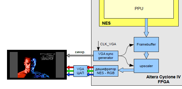
NES forms a picture with a resolution of 256x240 pixels. To display the image, I use the standard resolution of VGA 640x480. PPU renders the image into a frame buffer. Data from the frame buffer enters the block in which the resolution is doubled (upscaler). In the future I want to implement hq2x. Before applying data to the video DAC, the color is converted to RGB.
DMA controller
To quickly fill in OAM, the NES processor can use the DMA controller. The DMA controller is implemented very simply. Before starting the copy operation, the CPU must set the OAM start address (register 0x2003), or rather reset it to 0. Then the CPU writes to the address 0x4014 the value of the start address (0x ?? 00) in the address space of the CPU. The DMA controller stops the CPU and starts copying 256 bytes from the area 0x ?? 00 - 0x ?? FF (where ?? is the value specified by the CPU) to the PPU register 0x2004. The PPU increments the OAM address by one for each write operation. At the end of the procedure, the DMA returns control to the CPU.
Priority and Sprite 0 Hit
The final pixel color value is formed as follows:
It is quite possible and often happens that more than one sprite is in the same area.
In this case, the priority of the output to the screen is affected by two factors - this is the value of the sprite address in OAM and the priority flag (0 - foreground, 1 - background). For example, a sprite in which the priority flag indicates that it belongs to the background, but the value of the address in OAM is less than that of the foreground sprite, then the background sprite can close the front sprite, which will lead to the output of the background pixel, but only if it is not transparent.
When rendering the first opaque pixel of the sprite with address 0 (the background at this point should also be opaque), a flag is raised in register 0x2002 indicating that the Sprite 0 hit event has occurred. An example of the application of this flag is the Super Mario Bros. 1, in it it is used to break the screen and separate static information about points and time from the playing area. The coin image serves as the background, and its shadow as the zero sprite. The CPU periodically checks the value of the flag, and when an event occurs, the output of the playing field begins.
Interruption from the mapper MMC 3
Mapper MMC3 includes a line counter, the value of which decreases when the next PPU line is displayed. Upon reaching zero, the counter is reloaded with a value that can be set by pre-writing to the corresponding register of the mapper and, if the enable flag is set, a CPU interrupt occurs. The counter clocking line is organized in a rather original way - it is connected to the address line A12 of the GPU. For storing background tiles, the lower bank is usually used (region 0x000 - 0x0FFF), and for sprites, the senior bank (region 0x1000 - 0x1FFF). When drawing a visible line, PPU refers to one bank, and when fetching sprite image data in HBLANK, the period refers to another. Therefore, the frequency on line A12 will correspond to the line output frequency.
You can look at examples on video.
APU
The NES audio processor is on the same chip as the CPU. Functionally, the APU is a set of control registers, a frame counter and 5 blocks of audio channels.
From a hardware point of view, the APU is a bunch of counters, there are no pitfalls there, so the description will be brief.
The frame counter generates clock pulses with a frequency of approximately 240 Hz, 120 Hz for APUs, as well as IRQ interrupt for the CPU. Interrupt generation can be turned off by setting APU registers. The concept of “frames” should not be confused, in this case it has nothing to do with PPU.
By the way, an unpleasant incident occurred during development, the APU frame counter was already implemented and I messed up the interrupt enable flag (it turned out to be inverted), so the interrupt was generated with a frequency of about 60 Hz. Outwardly, this manifested itself very unexpectedly - in the game “Prince of Persia”, on the left side of the screen, the doorway with a grill was not displayed, and this was the only graphic artifact. I broke my head until I found the real reason. And I thought, of course, on PPU - I checked the code a hundred times, looking in ModelSim. It was unpleasant!
The APU has five channels:
Two rectangular channels, as the name implies, they form a square wave, one triangular channel, one noise channel and a delta modulation channel (DMC).
Rectangular channels can form a signal with variable duty cycle (4 gradations) and a period, with the ability to set the duration, and also have sweep and envelope blocks. The sweep block can change (sequentially increase or decrease) the signal period in time, and the envelope block (envelope) - reduce the signal amplitude in time with the possibility of looping, the envelope shape in this case is sawtooth.
The triangular channel generates a triangular signal with a variable frequency and duration, however, it does not have the ability to adjust the volume.
The noise channel generates a pseudo-random signal with a variable duration. As well as a rectangular channel, the noise channel has an envelope control unit.
The channel of delta modulation in the project has not yet been implemented.
Mixing of channels is carried out in a tabular way, so as not to use “heavy” operations in terms of consumption of LE.
After mixing, the signal enters the domain synchronization block and the filter, after which it goes to the WM8731 audio codec via the I2S serializer block.
When implementing the project, I used the Verilog 2001 hardware description language.
Anticipating questions regarding the source code, I can say that, since this is my first big FPGA project, I probably implemented many things in a very inefficient way. In addition, this is the very first version, the code needs to be optimized and cleaned up, because I rewrote many blocks several times. Therefore, I would not want to provide it in this form. If I find the time, get together and put the code in order, then maybe it will be posted under the GNU GPL license.
Thanks for attention!