SamsPcbGuide Part 7: Tracing Signal Lines. Differential pairs
This is the seventh article from the cycle and the last in the block on the tracing of signal lines. Then there is an idea to develop the project and go to the manual for the design of printed circuit boards in the form of a convenient book, so it is possible for publications. there will be a pause. The article deals with an important topic - the differential data transfer scheme, which is becoming more and more common in modern systems, and offers recommendations on the tracing of differential pairs, allowing to ensure the advantages of this scheme.
In the previous one , it was shown that the cross connection between independent signal lines is a source of unwanted interference. However, in the case of a differential transmission scheme, a strong cross connection, on the contrary, makes the signal more resistant to interference. In this scheme, two lines are used (differential pair), the signal sources of which are out of phase, and the receiver reacts to the voltage difference on the V lines DIFF = V + -V - (Fig. 1). The common mode signal (English common signal) is defined as V COMM = 1/2 ∙ (V + + V - ) and may be non-zero, for example, as in the widespread LVDS standard. Differential pair is characterized by two resistances:


The introductory theory of differential signaling is described in many sources, for example, in [1]. From the point of view of the design of printed circuit boards, it is important to dwell on the advantages of the differential circuit with respect to the asymmetric (eng. Single-ended) and on the requirements for the topology of differential pairs that provide these advantages.
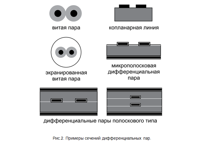
First of all, the ideal differential pair is symmetric, that is, throughout the entire length, its cross section should be constant and have an axis of symmetry (Fig. 2). This, as well as in the case of an asymmetric transmission line, ensures the constancy of the characteristic impedance of the differential pair, which significantly reduces line reflections and signal distortion.

Reducing the distance between the lines to s≤2 h results in a significant increase in the mutual coupling and overlapping of the distributions of the return currents in the supporting layer (Fig. 3-B). Such a differential pair is called a tightly coupled differential line. Differential impedance becomes more dependent on the distance between tracks. Its value decreases, therefore, to maintain the previous value, narrower paths are required, which slightly increases ohmic losses. However, it is this topology of the differential pair that provides the following advantages with respect to the asymmetric line:
These advantages should be called potential benefits, because they are fully realized only when two conditions are met simultaneously:
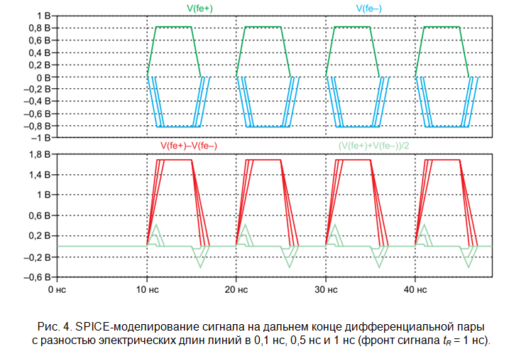
If you do not take into account the non-ideality of the signal source, then the first requirement is ensured by compliance with recommendation P.1 and coordination of both differential and common-mode signals on the load side. However, in practice, due to the limitations imposed by the location and geometry of the contact pads of components and vias, the need for turns, the strict constancy of the cross section of a differential pair is difficult to implement, which is also expressed in the difference in the lengths of lines of the pair. The difference in lengths of the pair leads to a phase run, distorting the differential signal and interfering with the common-mode signal (Fig. 4).
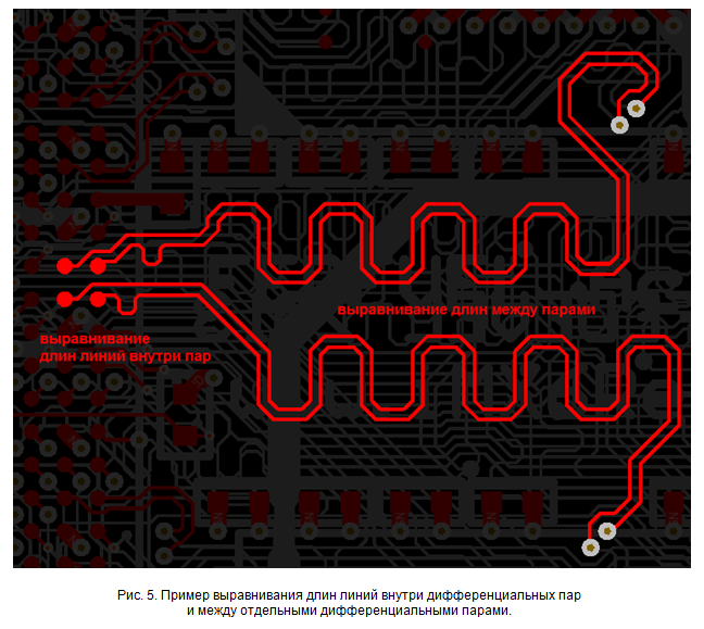
A common practice of aligning the lengths of lines (born length matching, tuning) is to increase the length of the shorter lines due to the additional bends that can form a regular structure (Fig. 5). It is obvious that in this case the distance between the lines of the pair inevitably changes. This, in turn, leads to a local change in the impedance of the pair and the occurrence of reflections. D. Brooks in one of the articlessuggests that the task of aligning the lengths of a pair of lines is of greater importance in terms of signal integrity and EMC. And the choice of bending geometry is not critical, with the only proviso that long and narrow bends are not recommended, as they can lead to distortions due to the strong interconnection of sections. However, this thesis is not a universal rule. The fact is that there is a more advanced method of aligning the lengths of the lines, which consists in simultaneously maintaining the impedance of the pair in places of bends (due to changes in the width of the lines, the use of local cuts in the support layer, etc.). However, the construction of such alignment geometry is a rather complicated task, requiring the use of specialized CAD systems, and is justified only for gigahertz signal lines. Another option is a local increase in the distance between the lines of the pair and alignment due to bends on one of the lines. In other words, the implementation of a local transition to a differential pair with a weak coupling, for which the impedance is not so strongly dependent on the distance between the lines (which is observed in places of bends). Examples and more detailed information on these techniques can be found in the materials presented on the website of Simberian, Inc.
The criterion of a sufficient degree of equality of the lengths of the lines is given in [1]: “The lengths of the lines of the differential pair must be aligned with each other with an accuracy of ∆L <0.1 ∙ t R ∙ v. It is recommended that the alignment section be located in the part of the differential pair where the symmetry is already broken (for example, by the location of the IC pins). ” By analogy with asymmetric lines, the influence of local inhomogeneity of the differential impedance is smaller, the shorter the electrical length of the equalization section is compared to the duration of the signal front.
The task is complicated by the fact that the alignment works fine only for a strip line, for which the propagation speeds of the common-mode and differential signals are equal. For a microstrip line, even the perfect alignment of the lengths of the lines of a pair does not ensure the absence of distortion, but is only a method of reducing them. But since the strip line requires a transition to the inner layers with the use of vias, which themselves are heterogeneous, it cannot be said for sure that the microstrip line has no advantages. Of course, the significance of these effects increases with increasing upper bound of the frequency band of the signal. And if at frequencies below 1 GHz, the alignment provides a low level of distortion,
Common mode interferences can occur as in the differential pair itself due to any asymmetry of it, and so can be induced from other signal lines. It is impossible to eliminate distortions, but by matching the line, which prevents the occurrence of repeated reflections and oscillations, one can minimize their consequences. The main methods for matching the differential pair at the far end are presented in Table 1. The scheme without matching the common mode signal is simple and therefore is used quite often, however, in the presence of common mode noise in the lines, simplicity turns into potential problems. Unlike the differential signal, the common mode signal is a good source of EMR. Especially common mode noise becomes critical when using an unshielded twisted pair to transmit the signal,
Table 1. Signal line matching methods.
Notes:
1. When calculating the values of matching resistances, it is convenient to use the values of the impedance of even Z EVEN (eng. Even mode) and odd Z ODD (eng. Odd mode) operating modes of the differential pair. By definition, these are the impedance values of one of the lines in special modes of operation, when the signal is not distorted during propagation in a differential pair. In the case of a symmetrical pair of differential signals is equal to V + = V - for an even mode and antiphase signals V + = -V - for odd mode. At the same time, they are associated with the values of characteristic impedances of a differential pair by the following relations: Z DIFF = 2 ∙ Z ODD, Z COMM = 1/2 ∙ Z EVEN .
2. For a differential pair with a weak mutual coupling, Z ODD ≈ Z EVEN ≈ Z 0 and T-shaped matching schemes degenerate into a parallel matching scheme of each of the lines.
The differential scheme has many advantages relative to the asymmetric one and is fundamental for reliable and high-speed data transmission standards, including for systems with a large number of nodes. With the continuation of the clock growth rate, developers will have to deal more and more with the tracing of differential pairs, so this competence is strategically important and should be based not only on general recommendations, but supported by simulation results in specialized CAD systems and experimental data.
[1] Bogatin E. “Signal and power integrity - simplified”, 2nd ed., Pearson, 2010 The
article was first published in the journal Components and Technology 2018, No. 5. The publication on Habr is coordinated with the editors of the journal.
I again appeal to readers, of whom, after moving with “Geektimes,” he said less, for feedback, which can be expressed in comments, in personal messages, as you like. This applies to this article, and all previous ones. I would like to make a cool handy reference guide, with which someone will successfully start in the design of printed circuit boards with fewer errors, someone will deepen and improve their quality. Join us, constructively criticize, make a contribution to the development of the industry.
In the previous one , it was shown that the cross connection between independent signal lines is a source of unwanted interference. However, in the case of a differential transmission scheme, a strong cross connection, on the contrary, makes the signal more resistant to interference. In this scheme, two lines are used (differential pair), the signal sources of which are out of phase, and the receiver reacts to the voltage difference on the V lines DIFF = V + -V - (Fig. 1). The common mode signal (English common signal) is defined as V COMM = 1/2 ∙ (V + + V - ) and may be non-zero, for example, as in the widespread LVDS standard. Differential pair is characterized by two resistances:
The introductory theory of differential signaling is described in many sources, for example, in [1]. From the point of view of the design of printed circuit boards, it is important to dwell on the advantages of the differential circuit with respect to the asymmetric (eng. Single-ended) and on the requirements for the topology of differential pairs that provide these advantages.
First of all, the ideal differential pair is symmetric, that is, throughout the entire length, its cross section should be constant and have an axis of symmetry (Fig. 2). This, as well as in the case of an asymmetric transmission line, ensures the constancy of the characteristic impedance of the differential pair, which significantly reduces line reflections and signal distortion.
Each line of the differential pair has its own distribution of return current in the supporting layer. If the mutual connection between the lines of the pair is significantly less than their connection with the supporting layer, then the distribution of the return currents do not intersect (Fig. 3-A). Such a differential pair is called a loosly coupled differential line (weak coupling) differential pair. Since the distribution of high-frequency components of the signal is concentrated in the reference layer in the region of ± 3 ∙ h, a practical criterion for weak coupling is the condition that the distance between the edges of the printed tracks is s> 6 ∙ h or s> 3 ∙ w. Since the differential impedance of a pair with weak coupling is almost independent of the distance between the tracks Z DIFF ≈2 ∙ Z 0, then this distance may vary along the length of the line - for example, if there are obstacles in the path of the differential pair. This simplifies the requirements for the topology of a differential pair, but such lines lack the main advantages of differential data transfer.R.1.
The cross section of a differential pair should be maximally (ideally mirror) symmetrically and uniformly throughout its length. Between the lines of the pair there should not be elements of the topology of other signal chains.
Reducing the distance between the lines to s≤2 h results in a significant increase in the mutual coupling and overlapping of the distributions of the return currents in the supporting layer (Fig. 3-B). Such a differential pair is called a tightly coupled differential line. Differential impedance becomes more dependent on the distance between tracks. Its value decreases, therefore, to maintain the previous value, narrower paths are required, which slightly increases ohmic losses. However, it is this topology of the differential pair that provides the following advantages with respect to the asymmetric line:
- Greater stability of the differential signal to induced interference, including cross-interference and interference in the reference layer. The proximity and symmetry of the lines leads to the fact that the induced noise on each of the lines is almost equal to V NOISE + ≈V NOISE - , therefore the differential interference is small V NOISE DIFF = V NOISE + -V NOISE - ≈0. This interference is the less, the farther from the differential pair is its source.
- Lower EMR and generated crosstalk. Since the signals V + and V - are in antiphase, the electromagnetic fields emitted by them are approximately equal in magnitude and have the opposite direction to each other. This leads to the fact that the superposition of fields in the far field tends to zero. The same effect significantly reduces the near-field crosstalk generated by the differential pair.
- Less impact of gaps in the bearing layer. The return currents I + and I - are also in antiphase, while due to the geometric symmetry of their distribution in the supporting layer are symmetrical. In this regard, the total current in the reference layer I REF = I + + I -decreases, and in the overlap region becomes equal to zero. In the case of complete overlap, when the differential pair is at a distance from the support layer h> 2 (s + w) and the interconnection of the lines significantly exceeds their connection with the support layer, there is no current in the support layer (Fig. 3B). Such a situation may arise, in particular, when a differential pair crosses a wide gap in the support layer. Despite the fact that the impedance at the intersection undergoes a local change, the distortion of the differential signal is small compared to the distortion of the asymmetric signal in such a case [1].
These advantages should be called potential benefits, because they are fully realized only when two conditions are met simultaneously:
- strict antiphase signals throughout the line,
- no common mode noise.
If you do not take into account the non-ideality of the signal source, then the first requirement is ensured by compliance with recommendation P.1 and coordination of both differential and common-mode signals on the load side. However, in practice, due to the limitations imposed by the location and geometry of the contact pads of components and vias, the need for turns, the strict constancy of the cross section of a differential pair is difficult to implement, which is also expressed in the difference in the lengths of lines of the pair. The difference in lengths of the pair leads to a phase run, distorting the differential signal and interfering with the common-mode signal (Fig. 4).
A common practice of aligning the lengths of lines (born length matching, tuning) is to increase the length of the shorter lines due to the additional bends that can form a regular structure (Fig. 5). It is obvious that in this case the distance between the lines of the pair inevitably changes. This, in turn, leads to a local change in the impedance of the pair and the occurrence of reflections. D. Brooks in one of the articlessuggests that the task of aligning the lengths of a pair of lines is of greater importance in terms of signal integrity and EMC. And the choice of bending geometry is not critical, with the only proviso that long and narrow bends are not recommended, as they can lead to distortions due to the strong interconnection of sections. However, this thesis is not a universal rule. The fact is that there is a more advanced method of aligning the lengths of the lines, which consists in simultaneously maintaining the impedance of the pair in places of bends (due to changes in the width of the lines, the use of local cuts in the support layer, etc.). However, the construction of such alignment geometry is a rather complicated task, requiring the use of specialized CAD systems, and is justified only for gigahertz signal lines. Another option is a local increase in the distance between the lines of the pair and alignment due to bends on one of the lines. In other words, the implementation of a local transition to a differential pair with a weak coupling, for which the impedance is not so strongly dependent on the distance between the lines (which is observed in places of bends). Examples and more detailed information on these techniques can be found in the materials presented on the website of Simberian, Inc.
The criterion of a sufficient degree of equality of the lengths of the lines is given in [1]: “The lengths of the lines of the differential pair must be aligned with each other with an accuracy of ∆L <0.1 ∙ t R ∙ v. It is recommended that the alignment section be located in the part of the differential pair where the symmetry is already broken (for example, by the location of the IC pins). ” By analogy with asymmetric lines, the influence of local inhomogeneity of the differential impedance is smaller, the shorter the electrical length of the equalization section is compared to the duration of the signal front.
The task is complicated by the fact that the alignment works fine only for a strip line, for which the propagation speeds of the common-mode and differential signals are equal. For a microstrip line, even the perfect alignment of the lengths of the lines of a pair does not ensure the absence of distortion, but is only a method of reducing them. But since the strip line requires a transition to the inner layers with the use of vias, which themselves are heterogeneous, it cannot be said for sure that the microstrip line has no advantages. Of course, the significance of these effects increases with increasing upper bound of the frequency band of the signal. And if at frequencies below 1 GHz, the alignment provides a low level of distortion,
Common mode interferences can occur as in the differential pair itself due to any asymmetry of it, and so can be induced from other signal lines. It is impossible to eliminate distortions, but by matching the line, which prevents the occurrence of repeated reflections and oscillations, one can minimize their consequences. The main methods for matching the differential pair at the far end are presented in Table 1. The scheme without matching the common mode signal is simple and therefore is used quite often, however, in the presence of common mode noise in the lines, simplicity turns into potential problems. Unlike the differential signal, the common mode signal is a good source of EMR. Especially common mode noise becomes critical when using an unshielded twisted pair to transmit the signal,
Table 1. Signal line matching methods.
| Name and scheme | Loss level | Comments |
|---|---|---|
 | low |  |
 | tall |  |
 | tall | |
 | average |  |
Notes:
1. When calculating the values of matching resistances, it is convenient to use the values of the impedance of even Z EVEN (eng. Even mode) and odd Z ODD (eng. Odd mode) operating modes of the differential pair. By definition, these are the impedance values of one of the lines in special modes of operation, when the signal is not distorted during propagation in a differential pair. In the case of a symmetrical pair of differential signals is equal to V + = V - for an even mode and antiphase signals V + = -V - for odd mode. At the same time, they are associated with the values of characteristic impedances of a differential pair by the following relations: Z DIFF = 2 ∙ Z ODD, Z COMM = 1/2 ∙ Z EVEN .
2. For a differential pair with a weak mutual coupling, Z ODD ≈ Z EVEN ≈ Z 0 and T-shaped matching schemes degenerate into a parallel matching scheme of each of the lines.
The differential scheme has many advantages relative to the asymmetric one and is fundamental for reliable and high-speed data transmission standards, including for systems with a large number of nodes. With the continuation of the clock growth rate, developers will have to deal more and more with the tracing of differential pairs, so this competence is strategically important and should be based not only on general recommendations, but supported by simulation results in specialized CAD systems and experimental data.
Literature
[1] Bogatin E. “Signal and power integrity - simplified”, 2nd ed., Pearson, 2010 The
article was first published in the journal Components and Technology 2018, No. 5. The publication on Habr is coordinated with the editors of the journal.
PS
I again appeal to readers, of whom, after moving with “Geektimes,” he said less, for feedback, which can be expressed in comments, in personal messages, as you like. This applies to this article, and all previous ones. I would like to make a cool handy reference guide, with which someone will successfully start in the design of printed circuit boards with fewer errors, someone will deepen and improve their quality. Join us, constructively criticize, make a contribution to the development of the industry.