Samsung introduced the Exynos 9 8895 mobile chip - 8 cores, 10 nm, gigabit LTE

While manufacturers of desktop processors cannot master the 10 nm process technology while continuing to produce the most powerful processors using the 14 nm process technology, other electronics manufacturers have already overcome this technological milestone.
On February 23, 2017, Samsung introduced the latest generation of high-performance on-chip systems (SoC, SoC) - Exynos 8895 , the first SoC designed by Samsung for a 10-nm design process (FinFET). This SoC determines the technical characteristics of the most powerful smartphones in the near future, maybe the next Galaxy S8 (April). Similar characteristics will be at the A11 chip in the iPhone 8 (September), the production of which is also on the 10-nm process technology involved TSMC.
Samsung has long been producing the Exynos SoC line, but recently it has clearly staked out its high-end leadership position, which was confirmed by the latest Exynos 7420 and Exynos 8890 chips manufactured using the 14nm process technology. By the way, Exynos 8890 became the first SoC, which is based on Samsung's own Exynos M1 microarchitecture. Compared to the standard ARM architectures, a number of changes and improvements have been made to it.
Exynos 8895 continues this tradition, it is also based on its own micro-architecture and M1 cores.
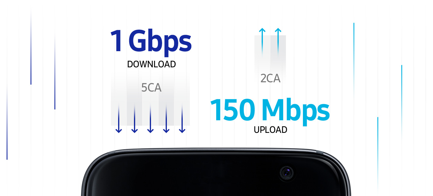
By the name of Exynos 8895 it is clear that it should not differ much from Exynos 8890, but still there are a number of pleasant changes. The most important thing, of course, is the transition to a 10 nm process technology. And in the technical specifications striking radical improvement in image processor (ISP). Signal processing from the front camera has been increased from a resolution of 13 MP to 28 MP at once. The main camera “grew up” from 24 MP to 28 MP, a “dual camera” mode appeared. The characteristics of the modem have improved, which now supports data reception at speeds up to 1 Gbit / s (LTE Cat16) - just like the future LTE modem of Qualcomm X20 .
Seriously improved graphics to Mali G71MP20. This graphics processor can calculate the virtual reality with a resolution of 4K, supports Vulkan API, OpenGL ES and OpenCL. New smartphones will be able to work on displays with a resolution of 3840 × 2400 and 4096 × 2160.
Clock frequencies of the central and graphic processor are not known yet.
Exynos SoC Specs
| SoC | Exynos 8895 | Exynos 8890 | Exynos 7420 |
|---|---|---|---|
| CPU | 4x A53 4x Exynos M2 (?) | 4x A53 @ 1.6 GHz 4x Exynos M1 @ 2.3 GHz | 4x A53 @ 1.5 GHz 4x A57 @ 2.1 GHz |
| GPU | Mali G71MP20 | Mali T880MP12 @ 650 MHz | Mali T760MP8 @ 770 MHz |
| Memory controller | 2x 32-bit (?) LPDDR4x | 2x 32-bit LPDDR4 @ 1794 MHz 28.7 GB / s b / w | 2x 32-bit LPDDR4 @ 1555 MHz 24.8 GB / s b / w |
| Storage | eMMC 5.1, UFS 2.1 | eMMC 5.1, UFS 2.0 | eMMC 5.1, UFS 2.0 |
| Modem | Receive: LTE Cat16 Transmission: LTE Cat13 | Receive: LTE Cat12 Transmission: LTE Cat13 | Unknown |
| ISP | Rear: 28 MP Front: 28 MP | Rear: 24 MP Front: 13 MP | Rear: 16 MP Front: 5 MP |
| Technical process | Samsung 10 nm LPE | Samsung 14 nm LPP | Samsung 14 nm LPE |
Due to the transition to the 10 nm LPE process technology, it was possible to achieve a performance increase of 27% and reduce energy consumption by 40% relative to 14 nm. True, the company does not explicitly indicate that improvements in these two parameters have been achieved simultaneously . A more realistic assessment seems to be about improving performance or reducing energy consumption.
The eight-core Exynos 8895 contains four high-performance “second-generation” cores (M2?) And four energy-efficient cores. It is not yet known what specific changes have been made to the core of the “second generation” compared to M1.
Since the Cortex-A53 energy-efficient cores are also manufactured using the 10-nm process technology, while maintaining the same architecture, they should become quite tiny in size - after all, even at 14 nm they were less than 1 mm².
Exynos 8895 will be the first SoC from Samsung with support for a heterogeneous system architecture (Heterogeneous System Architecture, HSA). This means that the CPU and GPU modules work on the same bus with shared memory, which improves the performance of SoC and facilitates programming. You no longer need to move data from the CPU memory to the GPU memory and back.
Samsung has introduced a more energy efficient memory LPDDR4x, which is an extension of the standard LPDDR4. Its power consumption has been reduced by 20% by reducing the output voltage I / O VDDQ by 45%, that is, from 1.1 V to 0.6 V. LPDDR4x memory has just started to be produced, it is also supported by the recently announced Qualcomm Snapdragon 835.
Other improvements Samsung mentions the Multi-Format Codec (MFC) video decoder, which supports the latest HEVC and VP9 video formats with a decoding speed of 120 frames / s at a maximum resolution of 4K UHD.
In the end, Samsung has integrated into the Exynos 8895 a “security subsystem with a separate computing module” for authentication (recognition of the iris, fingerprints), mobile payments, and the like. According to the description, it sounds like Apple Secure Enclave.
Samsung announced that the mass production of Exynos 8895 has already begun, so the release of the Galaxy S8 is clearly not far off.