Multi-core DSP TMS320C6678. Operating cores: processor computing resources
We continue to consider the device multi-core DSP TMS320C6678. This article is devoted to the device operating processor cores. The core architecture is described briefly with an emphasis on comparing the C66x platform with earlier well-known C6000 models.
The operating core of the signal processor is the main element that directly implements computational actions aimed at implementing signal processing in accordance with the algorithm dictated by the program embedded in the processor. Multi-core processors of the TMS320C66xx family contain a set of operating cores, which is a prerequisite for a corresponding increase in the computing performance of the device compared to single-core processors. Next, we will consider one typical DSP core of the TMS320C66xx processor.
TMS320C66x processors are an evolution of the Texas Instruments C6000 signal processor platform. The fundamentals of building the architecture are the same, however, their capabilities and, in part, the interpretation of their functioning have undergone some modifications.
The core of the TMS320C66xx processor is built on an architecture with a very long instruction word (Very Long Instruction Word - VLIW - “Wi-Al-AI-Double-U”). Each core includes 8 parallel computing units (2 multipliers and 6 ALUs) and a register file of 64 32-bit registers. Compared with the latest models of processors in the TMS320C6000 line, the TMS320C66xx processors have the following features.
Thus, the main emphasis, in terms of processor computing resources, in the C66x architecture is on multicore and on the expansion of the capabilities of vector arithmetic. Due to this, computing performance is increased by more than 30 times (if we compare the TMS320C6455 processor with a clock frequency of 1.2 GHz and a performance of 9600 MMACS and the TMS320C6678 processor with a frequency of 1.25 GHz and a performance of 320 GMACS). The main computing capabilities of the TMS320C66x processors in comparison with the processors of the previous TMS320C674x floating-point family are summarized in Table 1.1. Note that performance, expressed as the number of multiplication operations with accumulation per second, does not fully reflect the processing power of the processor. Vector arithmetic imposes a number of restrictions on operands. One multiplier, realizing 16 multiplications per cycle, it’s not the same as 16 multiplicators, performing seemingly the same 16 multiplications per cycle. Not all tasks can be well supported by vector arithmetic. In such cases, the processor resources may be idle and the architecture gain will not be felt.
The architecture of the TMS320C66x processor core is shown in Figure 1.3. As with any digital signal processor, the TMS320C66xx DSP core includes a set of computing units, a register file, a program machine, program and data memory.
TMS320C66x processors contain a double set of computing units - one on side A (Data Path A); the other on side B (Data Path B). The set of computing units is classic and includes a .M multiplier, ALU .L, a .S shifter, and a .D data address generator. In modern DSPs, the functions of each of these blocks are significantly expanded and may partially overlap, however, to simplify understanding, it is convenient to use classical terminology. All blocks work in parallel, extracting operands from the registers of the register file (A / B Register File) and returning the result of the corresponding operation to one of the registers.
Before entering the register file for processing, the data is stored in the data memory internal or external (L1D, L2 Cache / SRAM, MSM SRAM, DDR3 SRAM). The processing results and intermediate data arrays are also recorded in the memory. The memory subsystem of the TMS320C66x processor will be considered separately in the corresponding section.
Data is processed in accordance with the program downloaded to the processor. During operation, the program is located in the program memory (L1P, L2 Cache / SRAM, MSM SRAM, DDR3 SRAM). A program machine is responsible for reading a program from memory (Instruction Fetch), decoding it (Decode), and distributing it to the corresponding executive elements (Dispatch).
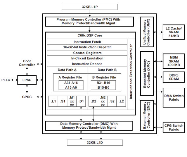
Figure 2 - C66x processor core architecture
Additional hardware modules in the processor core are a set of Control Registers, In-Circuit Emulation logic, an Interrupt and Exception Controller, a memory manager that includes a memory protection module (Program / Data Memory Controller), and a number of other components.
Next, we consider in more detail the computing units and registers of the operating kernel. In this case, we will focus only on the differences between the C66x core and the cores of previous processor models.
The C66x processors use the principle of packed instructions - the most frequently used instructions have a 16-bit length with a base length of 32 bits of the instruction word. This saves program memory. The processor software is able to extract, decode, and distribute up to 15 instructions simultaneously.
Register files of parties A and B contain 32 32-bit registers. It provides the ability to work with 8-, 16-, 32-, 64- and 128-bit data (for the fixed-point format), as well as with 40-bit data. The registers are grouped in pairs or fours.
The exchange bus between the register file and the computing units is expanded to 64 bits. Two 64-bit operands can be simultaneously applied to .L and .S blocks and a 64-bit result is obtained. The multiplier is supplied with two 128-bit operands, formed as two 64-bit input words. The result is 128-bit.
Only 64-bit words can be transmitted through the channels of intersection of sides A and B.
The ability to load operands from memory into registers has not changed - four 32-bit words per cycle. Memory write capabilities are expanded to four 32-bit words per clock cycle compared to TMS320C67x processors.
Commands are always 8 words from the memory, forming a sample packet. However, such a package can actually include up to 14 instructions due to the presence of 16-bit instructions packed in one word.
If the packet contains only regular 32-bit instructions, then every 0th bit of the instruction indicates in parallel that instruction is executed from the next or the next instruction is executed one clock cycle later. That is, the presence of a parallelism bit allows you to specify which of the commands are executed in parallel. As a result, execution packages are generated that can contain from 1 to 8 and 32-bit instructions.
If the sample packet includes packed commands, then such a packet is accompanied by a heading that occupies the 2 high words. The header indicates what is contained in the package, which of the commands are 16-bit, and which of the commands are executed in parallel.
Addressing is done similarly to earlier processor models. It is interesting, however, to note that for cyclic addressing, the possibility of looping out of alignment addresses is implemented.
The operation of the pipeline when processing commands as a whole does not differ from the general approach to organizing program execution for the C6000 platform. The pipeline includes 4 stages of command fetching, 2 stages of decoding and from 1 to 10 stages of command execution. Different commands execute different numbers of measures. Commands that are executed in one stage of execution are called single-cycle. Single-cycle commands include most fixed-point operations. Floating-point commands, even the basic operations of multiplication and addition, are 4-cycle commands. Memory access instructions, transition instructions, and many others are not single-ended. The difference in the execution time of different commands leads to various restrictions on the sharing of commands and processor resources. All this makes the processor programming process, especially at a low level, a rather difficult task. However, this concept, as already mentioned, lies at the heart of the entire C6000 platform.
Work with interrupts is organized similarly to other models of C6000 processors. Types of interrupts: restart, non-maskable interrupt, maskable interrupt and exception. The address of the interrupt vector table is indicated in a special register. The table contains a set of codes for each of the interrupts. If interrupt handling is simple, all relevant code can be written directly to the table itself. If the code does not fit, it is necessary to organize the transition to the interrupt processing procedure.
Usually, when responding to an interrupt, other masked interrupts are disabled. However, it is artificially possible to organize nested interrupt handling due to special code fragments described in the documentation.
All articles in the series:
The operating core of the signal processor is the main element that directly implements computational actions aimed at implementing signal processing in accordance with the algorithm dictated by the program embedded in the processor. Multi-core processors of the TMS320C66xx family contain a set of operating cores, which is a prerequisite for a corresponding increase in the computing performance of the device compared to single-core processors. Next, we will consider one typical DSP core of the TMS320C66xx processor.
TMS320C66x processors are an evolution of the Texas Instruments C6000 signal processor platform. The fundamentals of building the architecture are the same, however, their capabilities and, in part, the interpretation of their functioning have undergone some modifications.
The core of the TMS320C66xx processor is built on an architecture with a very long instruction word (Very Long Instruction Word - VLIW - “Wi-Al-AI-Double-U”). Each core includes 8 parallel computing units (2 multipliers and 6 ALUs) and a register file of 64 32-bit registers. Compared with the latest models of processors in the TMS320C6000 line, the TMS320C66xx processors have the following features.
- The number of multiplication and accumulation operations performed per cycle has been increased 4 times for both fixed and floating points. Each core is capable of performing 32 multiplications of 16x16 bits with a fixed point or 8 multiplications of 32x32 bits in a floating point format in one clock cycle.
- Increased efficiency of floating-point arithmetic: implemented support for the quick implementation of basic floating-point operations; floating-point calculations in SIMD mode (parallel actions on parts of data words); complex multiplication in floating point format; other functional extensions.
- The capabilities of vector arithmetic are expanded in both fixed and floating point formats. Vector arithmetic means the following concept. The operands at the input of arithmetic blocks are represented by 128-bit vectors consisting of 4 32-bit; 8 16-bit or 16 8-bit data words. Arithmetic operations can be performed simultaneously on all operands in vectors (SIMD mode). An example of vector multiplication using the QMPY32 command is shown in Figure 1.

Figure 1 - An example of vector multiplication - There are additional special instruction sets for complex and matrix arithmetic. This functionality is similar to vector multiplication, however, instead of the SIMD mode, more complex schemes are used that allow, in particular, to implement up to two complex multiplications of a vector of dimension (1x2) and a matrix of dimension (2x2) per cycle. Additional operations are also supported, such as, for example, taking a complex conjugate number.
Thus, the main emphasis, in terms of processor computing resources, in the C66x architecture is on multicore and on the expansion of the capabilities of vector arithmetic. Due to this, computing performance is increased by more than 30 times (if we compare the TMS320C6455 processor with a clock frequency of 1.2 GHz and a performance of 9600 MMACS and the TMS320C6678 processor with a frequency of 1.25 GHz and a performance of 320 GMACS). The main computing capabilities of the TMS320C66x processors in comparison with the processors of the previous TMS320C674x floating-point family are summarized in Table 1.1. Note that performance, expressed as the number of multiplication operations with accumulation per second, does not fully reflect the processing power of the processor. Vector arithmetic imposes a number of restrictions on operands. One multiplier, realizing 16 multiplications per cycle, it’s not the same as 16 multiplicators, performing seemingly the same 16 multiplications per cycle. Not all tasks can be well supported by vector arithmetic. In such cases, the processor resources may be idle and the architecture gain will not be felt.
| C674x | C66x | |
|---|---|---|
| The number of multiplications with accumulation per cycle in the format 16x16 bit fixed-point | 8 | 32 |
| The number of multiplications with accumulation per cycle in the format 32x32 bit fixed-point | 2 | 8 |
| The number of multiplications accumulated per cycle in the usual precision floating-point format | 2 | 8 |
| The number of common floating point operations per cycle | 6 | sixteen |
| Read / write bandwidth between core and memory | 2x64 bits | 2x64 bits |
| Dimension of vector operands (SIMD processing capabilities) | 32 bits (2x16 bit, 4x8 bit) | 128 bits (4x32 bits, 4x16 bits, 4x8 bits) |
The architecture of the TMS320C66x processor core is shown in Figure 1.3. As with any digital signal processor, the TMS320C66xx DSP core includes a set of computing units, a register file, a program machine, program and data memory.
TMS320C66x processors contain a double set of computing units - one on side A (Data Path A); the other on side B (Data Path B). The set of computing units is classic and includes a .M multiplier, ALU .L, a .S shifter, and a .D data address generator. In modern DSPs, the functions of each of these blocks are significantly expanded and may partially overlap, however, to simplify understanding, it is convenient to use classical terminology. All blocks work in parallel, extracting operands from the registers of the register file (A / B Register File) and returning the result of the corresponding operation to one of the registers.
Before entering the register file for processing, the data is stored in the data memory internal or external (L1D, L2 Cache / SRAM, MSM SRAM, DDR3 SRAM). The processing results and intermediate data arrays are also recorded in the memory. The memory subsystem of the TMS320C66x processor will be considered separately in the corresponding section.
Data is processed in accordance with the program downloaded to the processor. During operation, the program is located in the program memory (L1P, L2 Cache / SRAM, MSM SRAM, DDR3 SRAM). A program machine is responsible for reading a program from memory (Instruction Fetch), decoding it (Decode), and distributing it to the corresponding executive elements (Dispatch).
Figure 2 - C66x processor core architecture
Additional hardware modules in the processor core are a set of Control Registers, In-Circuit Emulation logic, an Interrupt and Exception Controller, a memory manager that includes a memory protection module (Program / Data Memory Controller), and a number of other components.
Next, we consider in more detail the computing units and registers of the operating kernel. In this case, we will focus only on the differences between the C66x core and the cores of previous processor models.
The C66x processors use the principle of packed instructions - the most frequently used instructions have a 16-bit length with a base length of 32 bits of the instruction word. This saves program memory. The processor software is able to extract, decode, and distribute up to 15 instructions simultaneously.
Register files of parties A and B contain 32 32-bit registers. It provides the ability to work with 8-, 16-, 32-, 64- and 128-bit data (for the fixed-point format), as well as with 40-bit data. The registers are grouped in pairs or fours.
The exchange bus between the register file and the computing units is expanded to 64 bits. Two 64-bit operands can be simultaneously applied to .L and .S blocks and a 64-bit result is obtained. The multiplier is supplied with two 128-bit operands, formed as two 64-bit input words. The result is 128-bit.
Only 64-bit words can be transmitted through the channels of intersection of sides A and B.
The ability to load operands from memory into registers has not changed - four 32-bit words per cycle. Memory write capabilities are expanded to four 32-bit words per clock cycle compared to TMS320C67x processors.
Commands are always 8 words from the memory, forming a sample packet. However, such a package can actually include up to 14 instructions due to the presence of 16-bit instructions packed in one word.
If the packet contains only regular 32-bit instructions, then every 0th bit of the instruction indicates in parallel that instruction is executed from the next or the next instruction is executed one clock cycle later. That is, the presence of a parallelism bit allows you to specify which of the commands are executed in parallel. As a result, execution packages are generated that can contain from 1 to 8 and 32-bit instructions.
If the sample packet includes packed commands, then such a packet is accompanied by a heading that occupies the 2 high words. The header indicates what is contained in the package, which of the commands are 16-bit, and which of the commands are executed in parallel.
Addressing is done similarly to earlier processor models. It is interesting, however, to note that for cyclic addressing, the possibility of looping out of alignment addresses is implemented.
The operation of the pipeline when processing commands as a whole does not differ from the general approach to organizing program execution for the C6000 platform. The pipeline includes 4 stages of command fetching, 2 stages of decoding and from 1 to 10 stages of command execution. Different commands execute different numbers of measures. Commands that are executed in one stage of execution are called single-cycle. Single-cycle commands include most fixed-point operations. Floating-point commands, even the basic operations of multiplication and addition, are 4-cycle commands. Memory access instructions, transition instructions, and many others are not single-ended. The difference in the execution time of different commands leads to various restrictions on the sharing of commands and processor resources. All this makes the processor programming process, especially at a low level, a rather difficult task. However, this concept, as already mentioned, lies at the heart of the entire C6000 platform.
Work with interrupts is organized similarly to other models of C6000 processors. Types of interrupts: restart, non-maskable interrupt, maskable interrupt and exception. The address of the interrupt vector table is indicated in a special register. The table contains a set of codes for each of the interrupts. If interrupt handling is simple, all relevant code can be written directly to the table itself. If the code does not fit, it is necessary to organize the transition to the interrupt processing procedure.
Usually, when responding to an interrupt, other masked interrupts are disabled. However, it is artificially possible to organize nested interrupt handling due to special code fragments described in the documentation.
All articles in the series:
- Processor Architecture Overview
- Operating cores: processor computing resources