First steps with STM32 and mikroC compiler for ARM architecture - Part 1
As a student, I had to very closely generalize with microcontrollers, then it was 8-bit 8051 and AVR. Now, wanting to return to this occupation, he turned his eyes to a very wide family of STM32 controllers. A lot has been written about them on the Web, nevertheless I expressed a desire to write a short series of articles about working with STMs. I would like to start acquaintance with them, as they say, from full 0. For experiments, I purchased a simple and cheap ($ 3) debugging card Maple Mini. The STM32F103CB controller used in it has a very impressive bunch of features. (especially in comparison with solutions in its price category). You can read in detail on the network, and of course, in the datasheet.. The native Arduin-like development environment did not immediately taste me (it tastes and color, as they say ...). Out of the abundance of diverse development environments, I turned my attention to mikroelektronika's mikroC for ARM. Once I came across their compilers (for 8081), I really liked it. Although not without jambs, but decided to try.
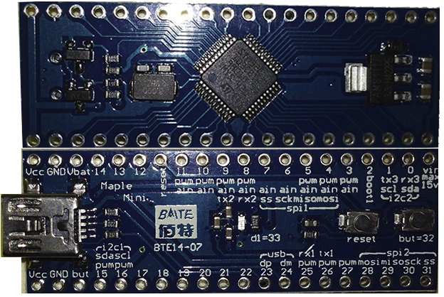
The board looks like this, everything is very simple and concise:
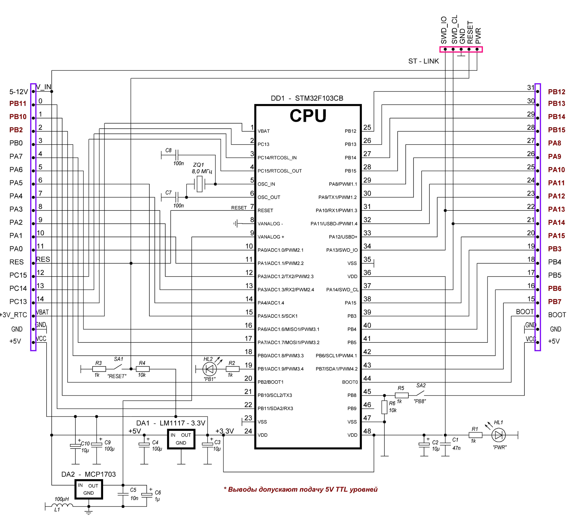
The circuit diagram of the board is also simple, but there is everything you need here:
The programmer selected the Chinese clone ST-LINK2 ($ 3), nevertheless it works great with mikroС

Link to the mikroC demo . Demo version limitation: maximum 4KB binary code. Not much, but enough for familiarization. There shouldn’t be any problems with installing the application, the only thing you need is to install the ST-LINK2 driver before starting the mikroC installer.
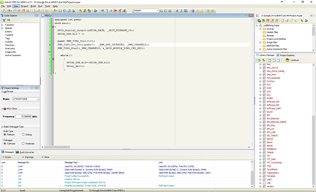
After starting and creating the project, we are greeted by the application window:
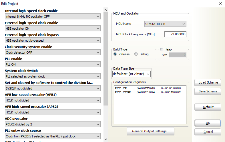
First of all, after choosing the type of microcontroller to use, you need to configure the properties of our project. The mikroC project configuration is invoked by the Shift-Ctrl-E (Project - Edit Project) keyboard shortcut . It is in this window that all the charms associated with the difficult internal organization of the STM32 clock system of microcontrollers are configured. In general, I advise you to at least briefly familiarize yourself with the Reference manual for this family of microcontrollers. We will return to it repeatedly.

Block diagram of a clock system from a datasheet STM32F103
In this window, the configuration of the registers RCC_CR and RCC_CFGR
- Internal high-speed clock enable - Enable or disable the internal 8MHz (HSI) generator (oscillator OFF)
- External high-speed clock enable - Enable or disable the internal 8MHz (HSE) generator (oscillator ON)
- External high-speed clock enable - Ability to connect to the OSC input of a clock generator instead of quartz. We tune to use quartz (HSE oscillator not bypassed)
- Clock seсurity system enable - Inclusion of the clock protection system integrated into the controller; not using yet (Clock detector OFF)
- PLL Enable - Enable / disable the frequency multiplier module (PLL ON)
- System clock switch - Selects the clock signal SYSCLOCK: PLL, external or internal oscillator. We use PLL. It is at the HSE frequency multiplied by the PLL coefficient that the core of our controller works (PLL selected as system clock)
- Set and cleared by software to control the division factor of the AHB clock - Install the SYSCLOCK pre-splitter for the AHB bus that services the peripheral modules of the MK; while disconnecting the pre-splitter * (SYSCLOCK not divided)
- APB low-speed prescaller APB1 - frequency divider for low-speed peripherals of MK, for example, I2C bus, maximum operating frequency: 36 MHz (HCLK divided by 2)
- APB high speed prescaller APB 2 - frequency divider for high-speed peripherals of MK, for example, input-output ports, timers, etc. (HCLK not devided)
- ADC prescaller - prescaler for the ADC module relative to APB 2 (PCLK2 divided by 2)
- PLL entry clock source - a clock source to the PLL input, either 1/2 of the built-in RC generator or an external generator passed through PREDIV1; and use it (Clock from PREDIV1 selected as the PLL input clock)
- HSE divider for PLL entry - setting this very PREDIV1; not using yet (HSE clock not divided)
- PLL multiplication factor - PLL multiplication factor. At the input we have a quartz frequency of 8 MHz, with a coefficient of 9 we have a frequency of 72 MHz for SYSCLOCK (PLL input clock x 9)
- USB prescaller - USB bus frequency. USB, according to the specification, operates at a frequency of 48 MHz, select the 1.5 splitter (PLL clock divided by 1.5)
MSU clock frequency, select the frequency SYSCLOCK - 72 MHz (72.000000)
Now we can save the settings for our MK. Everything is ready for writing 1 program. As always, we blink the LED (connected to the PB1 leg):
To set the GPIO port outputs to microC output there is a function
GPIO_Digital_Output(&GPIOх_BASE, _GPIO_PINMASK_ALL);// Настройка порта на выходit includes clocking of the GPIOx block and registers the values in the configuration register. The data that we write to the port is entered in the register GPIOx_ODR .
GPIOх_ODR = ; // Региcтр записи в портThe compiler allows you to access a specific bit of the register or variable. To do this, write the bit number (starting from 0) after the register name through the dot
REGx.by; // Доступ к отдельному (y) биту регистра (х)To generate delays, we use the built-in Delay_ms () (or Delay_us () ) function of the compiler. Here is our first program:
void main()
{
  GPIO_Digital_Output(&GPIOb_BASE, _GPIO_PINMASK_1);  //Делаем PB1 выходом
  GPIOb_ODR.b1 = 0; //Записываем в регистр GPIOb_ODR в 15 бит = 0
    while(1) // Бесконечный цикл
      {
        GPIOb_ODR.b1=~GPIOb_ODR.b1;  //Инверсия 15 бита
        Delay_ms(500); //Задержка 500 мс
      }
}
In order for one initialization command to be applied immediately to several port legs, we write _GPIO_PINMASKn via the "or" operator, for example:
GPIO_Digital_Output(&GPIOb_BASE, _GPIO_PINMASK_1 | _GPIO_PINMASK_7); //PB1 и PB7 настроены на выход
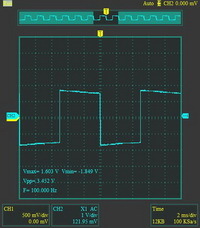
GPIO_Digital_Output(&GPIOa_BASE, _GPIO_PINMASK_ALL ); //Все ноги PA настроены на выходNow let's try to output the meander to one of the MK pins, switching the output state of port PB15 with an interval of 5 ms. :
void main()
{
  GPIO_Digital_Output(&GPIOb_BASE, _GPIO_PINMASK_15);
  GPIOb_ODR.b15 = 0;
   while(1)
      {
        GPIOb_ODR.b15=~GPIOb_ODR.b15;
        Delay_ms(5); // Задержка 5 мс.(Импульс 10 мс, частота 100 Гц)
      }
}
At pin PB15, we have the following signal:
If we need to read the status of the port, then we use the GPIOx_IDR register , after setting up the port for input using the GPIO_Digital_Input (* port, pin_mask) function. On our board there is a button connected to the output of the PB8 port. The following program lights a flashing LED on pin PB1 while the button is pressed.
void main()
{
  GPIO_Digital_Output(&GPIOb_BASE, _GPIO_PINMASK_1);
  GPIO_Digital_Input(&GPIOb_BASE, _GPIO_PINMASK_8); // Настраиваем вывод PB8 на вход
  GPIOb_ODR.b1 = 0;
    while(1)
      {
        if (GPIOb_IDR.b8) //Если кнопка нажата бит 8 регистра GPIOb_IDR равен 1
          {
           GPIOb_ODR.b1=~GPIOb_ODR.b1;
           Delay_ms(500); //Задержка 500 мс
          }
        else
          {
           GPIOb_ODR.b1 = 0; //Если кнопку отпустили, погасить светодиод
          }
      }
}
On this part 1 came to an end. In the second part, I will try to introduce you to the implementation of PWM modulation, working with timers and the function of suppressing contact bounce on the button.