MIPSfpga: out of canon
Over the past three weeks, seminars on the processor on the MIPSfpga FPGA have been held at MIET, MSU, MEPhI, MIPT and other Russian universities. In the framework of the seminars, laboratory work was carried out on which it was demonstrated how to put MIPSfpga into practice.
In the publication, I will talk about my experiments with MIPSfpga, which go beyond the scope of laboratory work, and consider the possibility of integrating the MIPSfpga processor core with IP blocks of opencores.org. I will also tell you about porting MIPSfpga to some Altera FPGA-based boards (Fmax values and FPGA resource usage indicators are given).
I want to make a reservation in advance that I am not at all an experienced FPGA hardware developer, and I began to master FPGAs precisely by working with MIPSfpga. Therefore, the presentation is carried out in a somewhat programmer-centric manner.
Background: What exactly is MIPSfpga
The MIPS Technologies company, the developer of the MIPS processor architecture, has a difficult fate: having started its work as an independent company in 1984, it managed to be part of Silicon Graphics (SGI), then regain independence, and in early 2013 become part of Imagination Technologies, in which quality and is at the time of writing this publication.
Processors with MIPS architecture are traditionally used to teach students the architecture of microprocessors, see, for example, the course of the MIPT-Intel laboratory .
MIPSfpga - is a MIPS32 processor core architecture of the family microAptivspecially designed for educational purposes. MIPSfpga is supplied as source code in Verilog, which makes it suitable for synthesis in FPGAs. It should be noted that at the time of this writing, access to MIPSfpga can only be obtained by students and university professors.
MIPSfpga is not a toy at all, this processor core is fundamentally no different from the microAptiv processor cores that Imagination supplies commercially.
The cores of the microAptive family, to which MIPSfpga belongs, can be classified as entry-level, and although these cores are not aimed at achieving record performance, they are fully software compatible with more advanced cores. The MIPSfpga core complies with the MIPS32 release 3 architecture, incorporates MMU (TLB) and cache memory. If desired, on MIPSfpga it is quite possible to run linux.
Along with the source MIPSfpga Imagination offers a training manual that sets out examples of how to work with MIPSfpga.
mipsfpga-plus: lab-on-a-chip system
Laboratory work (or simply labs) on MIPSfpga in Russia was carried out by Imagination employee Yuri Panchul. Yuri made tangible changes to the original materials of the works, primarily due to the fact that he had to adapt to the capabilities of universities in which labs were held.
For work, it is proposed to assemble a mipsfpga-plus system-on-chip, which includes the MIPSfpga core and a small strapping.
With some simplifications mipsfpga-plus structure is as follows:
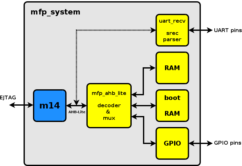
Figure m14 - CPU core MIPSfpga (also known as the core of the family M14Kc microAptiv ). For laboratory work, the interfaces with which the core is connected to the outside world are important: EJTAG and AHB-Lite.
The EJTAG interface is technological and is intended for debugging programs that run on the processor; more details about it can be found in the EJTAG publication : an attraction for hackers .
But the AHB-Lite interface is the main one for connecting the processor with the outside world. The AHB-Lite bus is a simplified version of the AHB bus, and, in particular, AHB-Lite allows only one request initiator ("master") on the bus. For details, refer to the AMBA 3 AHB-Lite Protocol v1.0 Specification (ARM IHI 0033A).
mfp_ahb-light decoder & mux(hereinafter referred to as a decoder ) is a block that decodes processor requests on the AHB-Lite bus and, depending on the address the processor addressed to, forwards the request to one of the IP blocks:- RAM
- boot RAM;
- GPIO
RAM is a memory block for storing programs and data;
boot RAM - a memory block that is completely similar in nature to a RAM block; the difference is that the boot RAM block contains a program that runs immediately after the RESET signal is removed (since this block is mapped to the address 0x1fc00000).
The GPIO block consists of a series of registers, the bits of which are connected to the LEDs and buttons / switches on the board; a program running on the processor core in this way can interact with the outside world.
For laboratory work, Yuri offers to output individual m14 signals to the LEDs of the board (such connections are situational in nature, and are not reflected in the figure).
This is how the decoder maps IP blocks to the physical addresses of the AHB-Lite bus:
| IP block | Base address | Length |
|---|---|---|
| RAM | 0x00000000 | 32K - 256K |
| GPIO | 0x1f800000 | 0x14 |
| boot RAM | 0x1fc00000 | 4K |
Attention: on the AHB-Lite bus, the processor core sets a physical address , which, as a rule, does not coincide with the address the program is operating on ( program address or virtual address ). For more information on the subtleties of addressing in MIPS, see the See MIPS Run book , Basic Address Space section.
During laboratory work, the processor performs test programs, which can be loaded into boot RAM in several ways.
The easiest option is to initialize boot RAM at the stage of creating the bitstream for the FPGA. On the one hand, it is very simple - uploaded the bitstream to the FPGA and the program starts to run. But on the other hand, if you want to make changes to the program, you will have to regenerate the bitstream again, which can be very expensive.
A more advanced way is to use the EJTAG debugging interface to download the program, however this method requires additional software and hardware - a JTAG adapter and openocd software (see an example of using EJTAG to load data into the RAM of a Black Swift board: geektimes.ru/post/249184 )
The YTAG adapter seemed to Yuri too exotic, therefore, especially for mipsfpga-plus in Verilog, he wrote an IP block that implements downloading data in S-record format via the UART interface (indicated as uart_recv srec parser in the figure ). In this case, to load data into boot RAM, it is enough to use an inexpensive USB-UART adapter and standard programs included with Linux or Windows. Immediately after switching on, the uart_recv block starts receiving data via the UART interface, while the processor core is stopped (the reset signal is active). After receiving data, the reset signal for the processor core is deactivated, and the uart_recv block is self-resetting.
For a more detailed description of mipsfpga-plus, see here .
Porting MIPSfpga
The canonical boards for MIPSfpga are the Terasic DE2-115 and Digilent Nexys4 DDR.

However, there are reasons that prompted me to work on porting MIPSfpga to other boards.
For example, I simply could not buy a Digilent Nexys4 DDR board. Here's what the Digilent site issued:

I received a negative response to a request to Terraelectronics about the possibility of buying a board from them.
As for the Terasic DE2-115 board, in my opinion its application for MIPSfpga is partly similar to firing sparrows from a gun: the FPGA is installed on the board with an excessive amount of resources for MIPSfpga, at the same time the cost of the board is quite high.
But most importantly, porting the project to new boards will allow you to better understand working with FPGAs and expand the list of boards suitable for laboratory work!
Portability Criteria
For testing, I conducted a synthesis of the reference project for the DE2-115 board:
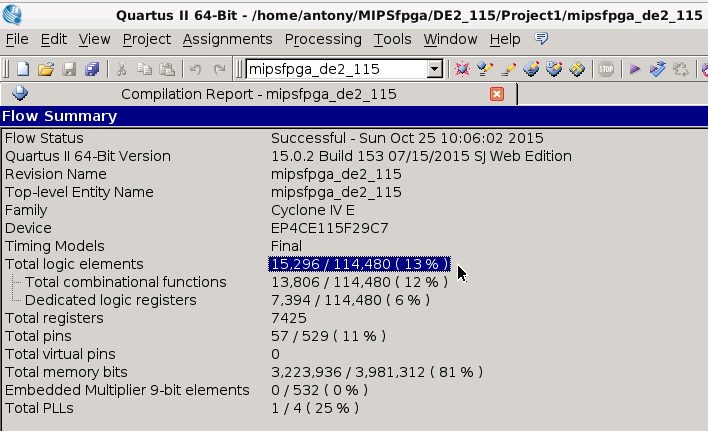
Let it not bother you that the project ate 3 Mbits of crystal memory - this value can be easily reduced. It is enough to reduce the block size of RAM and boot RAM. To save on-chip memory, FPGAs even have the opportunity to sacrifice part of the cache.
As can be seen from the presented report, about 15500 logical elements (LE) are required from FPGAs. This means that you need to focus on FPGAs with LEs over 20,000.
Let's try to find such cards.
Terasic Boards
The Taiwanese company Terasic offers a wide range of Altera FPGA based boards, and some boards purchased for educational purposes can be bought at a discount (Academic price):
 |  |  | |
|---|---|---|---|
| Pay | DE0-Nano | DE0-CV | DE1-SoC |
| FPGA | EP4CE22 | 5CEBA4F23 | 5CSEMA5F31 |
| family | Cyclone iv | Cyclone v | Cyclone V SoC |
| number of LE | 22K | 49K | 85K |
| memory, kbps | 594 | 3080 | 4450 |
| price | $ 79 | $ 150 | $ 249 |
| Academic price | $ 61 | $ 99 | $ 175 |
Fee Mars rover3
Inpro Plus LLC from Taganrog maintains an interesting site, marsohod.org , dedicated to the development of Altera FPGA devices. On the site you can buy the Mars rover3 board , which is quite suitable for MIPSfpga.
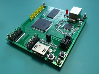
On the Mars rover3 board, the MAX10 FPGA for 50,000 LE with 1600 Kbps of memory is installed, and the board costs 8,000 rubles.
Connect IP blocks with opencores
Labs in which it is proposed to watch what is happening inside the processor core are quite useful and instructive. However, it would be more interesting to me to assemble my system-on-chip based on a real processor core from MIPS. This must be connected to the processor core by a number of peripheral devices. Interacting with the processor by pressing the buttons and looking at the LEDs is certainly good, but I want a more convenient interface. Almost all modern embedded systems use the UART interface for technological purposes, so I decided to add UART to mipsfpga-plus.
Writing from scratch an IP block that implements UART was not my goal, so I decided to use the ready one. It is no secret that opencores.org is the best-known site with free redistributable IP blocks. And of course there was an IP block that interested me. But here's the trouble - for free IP blocks, the standard bus is Wishbone, which is not compatible with the AHB-Lite MIPSfpga bus.
I tried to connect the UART IP block through the "adapter" AHB-Wishbone , which was found on opencores.org; I was counting on such a connection:
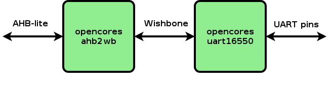
In practice, it turned out that the adapter did not work, as I was counting, so it turned out to be easier to modify the interface part of the UART IP block to support the AHB-Lite bus.
Since some software should work with the UART IP block, I borrowed the nmon nanomonitor from the barebox bootloader . nmon interacts with the user through UART and has only basic capabilities: it allows you to record / print a word at an address, as well as transfer control to an address.
However, nmon does not require RAM (sic!) For its work, it takes less than 1200 bytes, it works from any address in memory.
The small size allows you to put nmon in boot RAM immediately during synthesis. So now, right after removing the reset signal, the nmon prompt is issued to the UART interface, and the user can either use nmon to download and run programs, or manually write / read in the processor's address space, which can be useful for initial debugging of a user IP block. Typical nmon session:

To connect another IP block to AHB-Lite, you had to manually edit the decoder block. The final structure of mipsfpga-plus with a connected UART block looks like this:
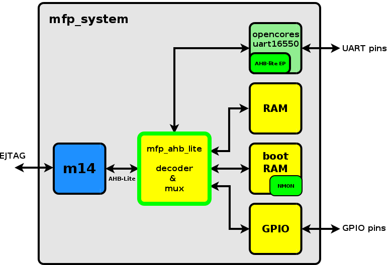
The final project, demonstrating how to connect a UART IP block with opencores to mipsfpga-plus, is called myMIPSfpga. myMIPSfpga works on Terasic DE0-Nano, DE0-CV, DE1-SoC boards, as well as on the Mars rover3 board.
The myMIPSfpga project is published on github: github.com/MIPSfpga/myMIPSfpga .
Using Free Software
Although Altera has to use the proprietary Quartus software to generate the bitstream for FPGAs (and there is nothing to be done about it), for many other tasks when working with MIPSfpga you can get by with freely distributed software.
To compile programs under MIPS, gcc and binutils software are used (you can use the pre-assembled toolchain Sourcery CodeBench Lite 2015.05-18 , or you can build your own using crosstool-ng ).
To work with the MIPS processor on EJTAG, openocd and gdb software are used. openocd can also be used to load bitstreams into the FPGA.
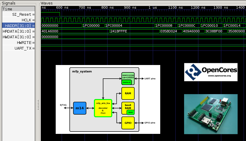
Icarus Verilog is quite suitable for modeling myMIPSfpga, and the timing diagrams based on the simulation results are quite convenient to consider using GtkWave:

myMIPSfpga: using FPGA resources
The seminar participants had questions about the FPGA resource utilization indicators, as well as the Fmax values for myMIPSfpga. Below I present the obtained values of Slow 1200mV 85C Model Fmax Summary in MHz, while the values for different versions of Quartus II software are given:
| Pay | FPGA | Quartus 13.1.4 | Quartus 15.0.2 |
|---|---|---|---|
| DE0-Nano | EP4CE22F17C6 | 31.66 | 31.22 |
| DE0-CV | 5CEBA4F23C7 | 31.24 | 34.06 |
| DE1-SoC | 5CSEMA5F31C6 | 28.24 | 37.17 |
| Mars rover3 | 10M50SAE144C8GES | --- | 06/27 |
But the indicators of the use of resources of different FPGAs:
| Characteristic | Quartus 13.1.4 | Quartus 15.0.2 |
|---|---|---|
| EP4CE22F17C6 | ||
| Total logic elements | 15.342 / 22.320 (69%) | 15,660 / 22,320 (70%) |
| Total combinational functions | 14,161 / 22,320 (63%) | 14,161 / 22,320 (63%) |
| Dedicated logic registers | 7.665 / 22.320 (34%) | 7.665 / 22.320 (34%) |
| Total registers | 7665 | 7665 |
| Total memory bits | 95.872 / 608.256 (16%) | 95.872 / 608.256 (16%) |
| 5CEBA4F23C7 | ||
| Logic utilization (in ALMs) | 7.283 / 18.480 (39%) | 6.972 / 18.480 (38%) |
| Total registers | 7976 | 8127 |
| Total block memory bits | 95.872 / 3,153,920 (3%) | 95.872 / 3,153,920 (3%) |
| 5CSEMA5F31C6 | ||
| Logic utilization (in ALMs) | 7.264 / 32.070 (23%) | 6.978 / 32.070 (22%) |
| Total registers | 7951 | 8104 |
| Total block memory bits | 95,616 / 4,065,280 (2%) | 95,616 / 4,065,280 (2%) |
| 10M50SAE144C8GES | ||
| Total logic elements | 37.206 / 49.760 (75%) | |
| Total combinational functions | 30,763 / 49,760 (62%) | |
| Dedicated logic registers | 25,165 / 49,760 (51%) | |
| Total registers | 25165 | |
| Total memory bits | 78,464 / 1,677,312 (5%) |
Note: Quartus 13.1.4 software does not support the MAX10 FPGA.
How could one use MIPSfpga with IP blocks with opencores
To conveniently work with opencores.org IP blocks, auxiliary tools have been created:
- fusesoc - a tool for controlling the assembly of a system-on-a-chip from separate IP blocks;
- wb_intercon - Wishbone switch generator.
fusesoc allows you to generate a system-on-a-chip using high-level descriptions, while fusesoc not only generates source code on Verilog, but also configuration files for CAD Altera or Xilinx.
wb_intercon allows you to generate the code for the Wishbone switch in Verilog; The configuration file with the parameters of the Wishbone ports and switching rules is used as input.
From experience gained when connecting a UART with a Wishbone bus to mipsfpga-plus, we can conclude that there will be a minimum of problems when assembling a system-on-chip from cores from opencores.org and MIPSfpga if the processor core itself is immediately connected to Wishbone.
Suppose you managed to make a normal adapter between AHB-Lite and Wishbone. Then the system-on-chip could look like this:
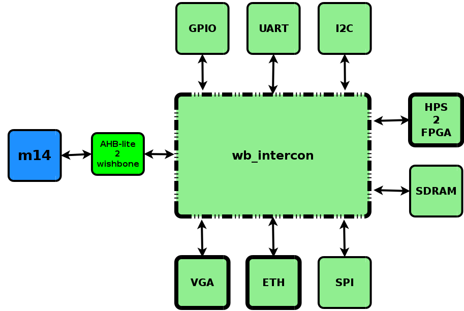
In the figure, GPIO, UART, I2C, VGA, ETH, SPI, SDRAM5, HPC2FPGA blocks are real IP blocks from opencores.org, the generated Wishbone switch is used to connect them to the microprocessor core.
Note: of course the AHB-Lite-in-Wishbone adapter will introduce additional delay; better performance can be achieved if Wishbone support is built into MIPSfpga. Moreover, following the example of OpenRISC cores, individual Wishbone buses for commands and data can be derived.
Afterword
Experience with MIPSfpga suggests that the initial development of FPGA-based systems-on-chip design is not something complicated, costly, and requires a lot of preparation. The availability of affordable motherboards with FPGAs, free CAD, freely distributed tools and manuals (I especially note the site marsohod.org) allows you to master the design of FPGAs even at home.
Acknowledgments
The author thanks Imagination employees Robert Owen and Yuri Panchul for the opportunity to work with MIPSfpga.
Special thanks to Nikolai Kovach and other authors of the site marsohod.org for the Mars rover3 fees, the ETF company for the Terasic DE1-SoC fee, and Alexey Zhukov for the DE0-Nano fee.
For help in developing Quartus II CAD systems, the author thanks the staff of the NIISI RAS: Sergey Aryashev, Andrey Shcherbakov, Alexander Kornilenko and Andrey Arakelov.
The author hopes that in the future the MIPSfpga license will be revised and this processor core will be available to all those interested in the architecture of microprocessors.