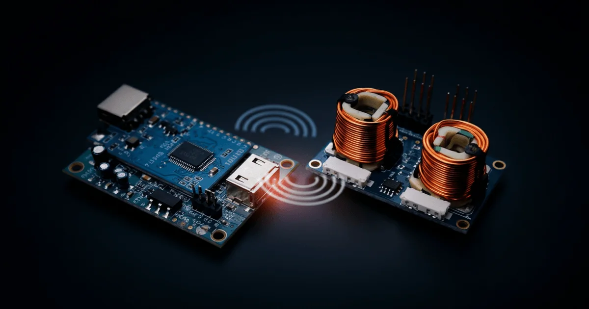
Implementing a Wireless Inductive Coupling Interface for Microcontrollers
When standard wireless modules (Wi-Fi, NFC, RFID) are unsuitable due to enclosure sealing requirements or specific application needs, inductive coupling offers an effective solution for short-range wireless data transmission. This article demonstrates how to create a reliable and compact wireless interface for configuration or data acquisition, operating at distances up to 10-15 centimeters, using basic electronic components like inductors, transistors, and a microcontroller.
Principles of Inductive Coupling and its Application in MCU Systems
Inductive coupling is a method of wireless energy or data transfer based on electromagnetic induction between two coils. This phenomenon is utilized in numerous devices, from transformers to wireless chargers and RFID systems. In the context of microcontroller systems, especially for applications requiring hermetic sealing or minimization of external interfaces, inductive coupling becomes an optimal choice. The absence of a need for an optical window (as with IR communication) or specific antennas for higher-frequency protocols allows such an interface to be integrated into even the most complex designs. The primary advantage lies in the ability to use standard microcontroller functions, such as UART, clock generator, and comparator, for signal generation and detection, minimizing the need for specialized chips. This approach is particularly relevant for embedded systems where cost, size, and power consumption play a crucial role.
Inductive Coupling Transmitter Design
At the heart of an inductive coupling wireless system is the transmitter, which converts a digital signal into radio frequency oscillations. In the proposed scheme, the microcontroller's clock frequency (e.g., PIC16F1823) is used as the carrier, and modulation is achieved using the UART output signal. For this, the clock frequency, output via the microcontroller's CLKOUT pin, is fed to a resonant circuit. However, since direct software control over CLKOUT is absent, additional circuitry is required.
The transmitter circuit uses two transistors (VT1, VT3) to modulate the carrier frequency. When the UART TX line is in a low logic state (logic 0), transistor VT1 turns on, and VT3 turns off, allowing the clock frequency to pass through resistor R3 to the coupling coil L2. This coil is inductively linked to the resonant circuit L3, C2, C5, which is tuned to the clock generator frequency and emits oscillations. When the UART TX is in a high logic state (logic 1), VT1 turns off, and VT3 turns on, blocking the carrier frequency from reaching the circuit. Thus, data is transmitted in an inverted form. The use of two transistors is necessary to prevent oscillation excitation due to the parasitic collector-emitter capacitance of a single transistor in its off state.
Component selection for the resonant circuit is critical. Coil L3 can be either a ready-made inductor (e.g., 470 µH) or a custom-wound one. An inductance of 500 µH on a "dumbbell" type DR2W 14x15 core showed good results, providing optimal circuit Q-factor. The core size affects the communication range, and inductance can vary between 200-500 µH. The coupling coil L2 typically has 5 turns of PEV-0.3 wire for an L3 inductance of 500 µH. Its inductance (0.5-3 µH) depends on the resonant impedance and Q-factor of the circuit.
Calculations for the resonant circuit:
- Resonant frequency:
f = 159 / √(L * C), where L is in µH, C in pF. - Characteristic impedance of the circuit:
p = √(L / C). - Approximate determination of coupling coil L2 inductance:
L2 = L3 Rn / (p Q), where Rn is the load resistance (330 Ohm), Q is the Q-factor.
Alternatively, inductive coupling can be replaced by capacitive coupling by omitting coil L2, but experimental tuning with a coupling coil often proves more convenient.
High-Sensitivity Inductive Coupling Receiver
Despite its critical role, the inductive coupling receiver path can be implemented with a minimal number of components. The presented receiver is based on a single transistor and functions as a high-sensitivity detector. Diode VD4 biases transistor VT7 at the threshold of conduction, significantly increasing the circuit's sensitivity. A distinctive feature of this implementation is its ability to rectify both positive and negative half-waves of the input voltage, thanks to diode VD3, which corresponds to the detector circuit proposed by V.T. Polyakov. A simpler half-wave rectification scheme is also possible, but this would lead to reduced sensitivity.
The detector's output voltage (DATA RX) varies: in the absence of an input signal, it is approximately 1.3-1.4 V, and with a maximum signal, it drops to 0.5-0.6 V. The detector's sensitivity reaches 7-10 mV (peak-to-peak value), at which point the output voltage will be around 0.9 V. The receiver's resonant circuit (L7, L6, C14, C15) should be identical to the transmitter's circuit for maximum efficiency.
The signal from the DATA RX detector output is fed to the microcontroller's comparator input. The microcontroller's internal Fixed Voltage Reference (FVR) is used as the comparator's reference voltage, typically set to 1.024 V. The comparator output (C1OUT) is then connected to the microcontroller's RX UART input, thus closing the wireless communication channel.
Example comparator configuration for a PIC microcontroller:
        //FVR
        FVRCON = 0b11000100; // Configure Fixed Voltage Reference
        //Comparator
        CM1CON0 = 0b10110010; // Enable comparator, select inputs
        CM1CON1 = 0b00100011; // Configure inversion, select reference voltage
The reliable communication range for such a transmitter-receiver pair is 10-15 cm. Sensitivity can be further enhanced by increasing the comparator's reference voltage, for example, to 1.2 V.
Building a Transceiver and Optimization Methods
Combining transmitter and receiver functions into a single transceiver significantly simplifies the design, allowing for the use of a common resonant circuit. This is achieved through circuit solutions that switch the circuit between transmit and receive modes. In the transceiver scheme, transistor VT6 is used to disable the detector during transmitter operation. This prevents high-frequency currents from flowing from the transmitter output into the base of the receiver path's transistor VT5, which could lead to incorrect operation or damage. The transceiver's resonant circuit (L4, L5, C4, C7) is constructed similarly to the previously described transmitter and receiver circuits.
Tuning all described circuits, whether a separate transmitter, receiver, or transceiver, boils down to precise adjustment of the resonant circuit. To do this, you need to:
- Connect an oscilloscope to the resonant circuit via a small capacitance (1-2 pF). A short piece of insulated wire can be used as a capacitor, with one end soldered to the circuit and the other (insulated) serving as the connection point for the oscilloscope probe.
- Turn on the transmitter (or the transceiver in transmit mode), making it generate pulses or continuously emit a signal (e.g., by setting DATA TX = 0).
- Rotate the trimmer capacitor (e.g., C7 for the transceiver circuit) until the maximum oscillation amplitude is achieved at 1 MHz. This ensures optimal energy and data transfer.
Operational Characteristics and Limitations
When working with a transceiver, several aspects are important to consider. During transmission, it is necessary to disable UART receiver interrupts and clear its register after transmission is complete. The receiver's recovery time after transmitter operation is approximately 100-200 µs. The maximum data transfer rate for such circuits typically does not exceed 5000-6000 bits/s and depends on the capacitance of capacitor C11 in the receiver path. The detector's bandwidth is about 3 MHz, which limits the use of excessively high microcontroller clock frequencies.
Since the system's selectivity is provided by a single resonant circuit with a relatively low Q-factor, it is critically important to place it as far as possible from potential sources of interference, such as mains wiring and switching power supplies, especially their inductive components. This will help minimize the impact of external noise and ensure stable operation of the wireless channel.
Key Takeaways:
- Inductive coupling is an effective solution for short-range (10-15 cm) wireless data transmission in sealed or compact devices.
- The system utilizes standard microcontroller functions (UART, CLKOUT, comparator) for signal modulation and demodulation.
- Transmitter and receiver can be combined into a transceiver with a common resonant circuit, requiring careful tuning.
- Key elements include resonant circuits with inductors (200-500 µH) and a high-sensitivity transistor-based detector.
- Data transfer speed is limited (up to 6000 bits/s), and the system is sensitive to electromagnetic interference from external sources.
— Editorial Team










No comments yet.