November 18, 2014 at 17:30
PDP Recovery 11/04
- Transfer
Translation of an article on the restoration of an old interesting machine. A lot of heavy pictures. Italics are my comments.
This PDP 11/04 was originally owned by Ericsson. We received it in the late eighties from EDKX - computer club Ericsson. The computer was handed over in parts, but everything was in place except for a couple of screws. Together with the PDP-11 itself was the TU60 tape station.
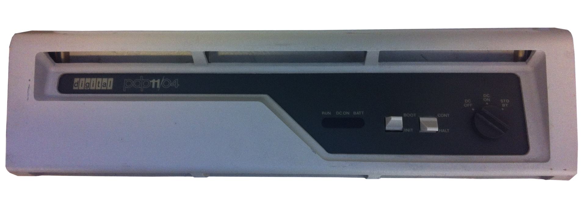
The
PDP-11/04 operator console panel appeared in the mid-seventies as the cheaper PDP-11/05 successor. In this new version, DEC was able to fit all the processor logic on one six-pin board (PDP used several types of boards with various form factors - six-pin, four-pin, two-pin. In the photo just below 6 groups of pins are visible. In addition, the boards were divided according to which bus they are designed for. ) instead of two in the predecessor. The modules were connected to a common cross-board ( backplate ) with nine slots performed by wrap-up. Typically, PDP 11 came with a programming console ( separate panel. PDP was assembled from several blocks. Something like a rack with a set of equipment ), through which the operator could enter simple boot programs and carry out system maintenance. However, this particular instance had only the usual limited operator console.
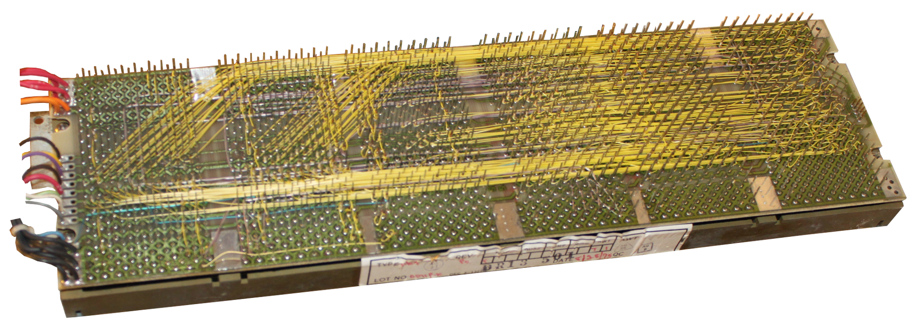
Cross Board
BookComputer Engineering: A DEC view of hardware design The PDP-11 family of machines is described in great detail. The book is scanned and is in the public domain. Very exciting reading!

CPU Board
The processor module consists of 138 chips. A slight simplification of the operational machine ( datapath, the part of the processor that performs operations on any data. For example, these are ALUs, multiplexers, register files, decoders. In general, this is practically the most important part of the processor.) and the use of programmable memory has reduced the number of chips used. The board has five 256x8 bipolar programmable ROM chips allocated for storing microcode, which is packed in 40-bit structures. The first eight bits are allocated to the address of the next microinstruction. An interesting feature is that the line along which these addresses are transmitted is implemented according to an open collector scheme, which allows conditional branching of microcode to be done simply using wired OR connections directly on the bus. As the main ALU, DEC took the well-known 74181, and Intel 3101 16x4 RAM chips were used as scratchpad memory for main registers. There is no separate crystal for clocking, but instead there is a delay line in the feedback circuit.

Memory
Card We got a PDP-11/04 with a 16 kilobyte memory module. It contains 32 MK4096, MOS dynamic memory chips produced by MOSTEK. An entertaining remark - this was the first memory with multi-addressing column / row addressing, a similar scheme is used in modern DDR. Thanks to this innovation, MOSTEK engineers were able to fit 4 kilobits of memory into a 16-pin package.
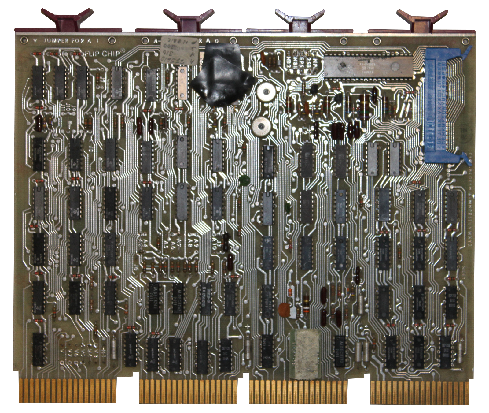
This is the M7800 card, DL11 asynchronous communications module. ( The PDP-11 used its own classification of modules. For example, the diagram indicates MS11-JP, which means a memory module, but specific boards could vary - M7867-XJ, M7847-DJ or some other card that complies with the module standard. In this case DL11 is a classifier, and the M7800 is a specific board. )
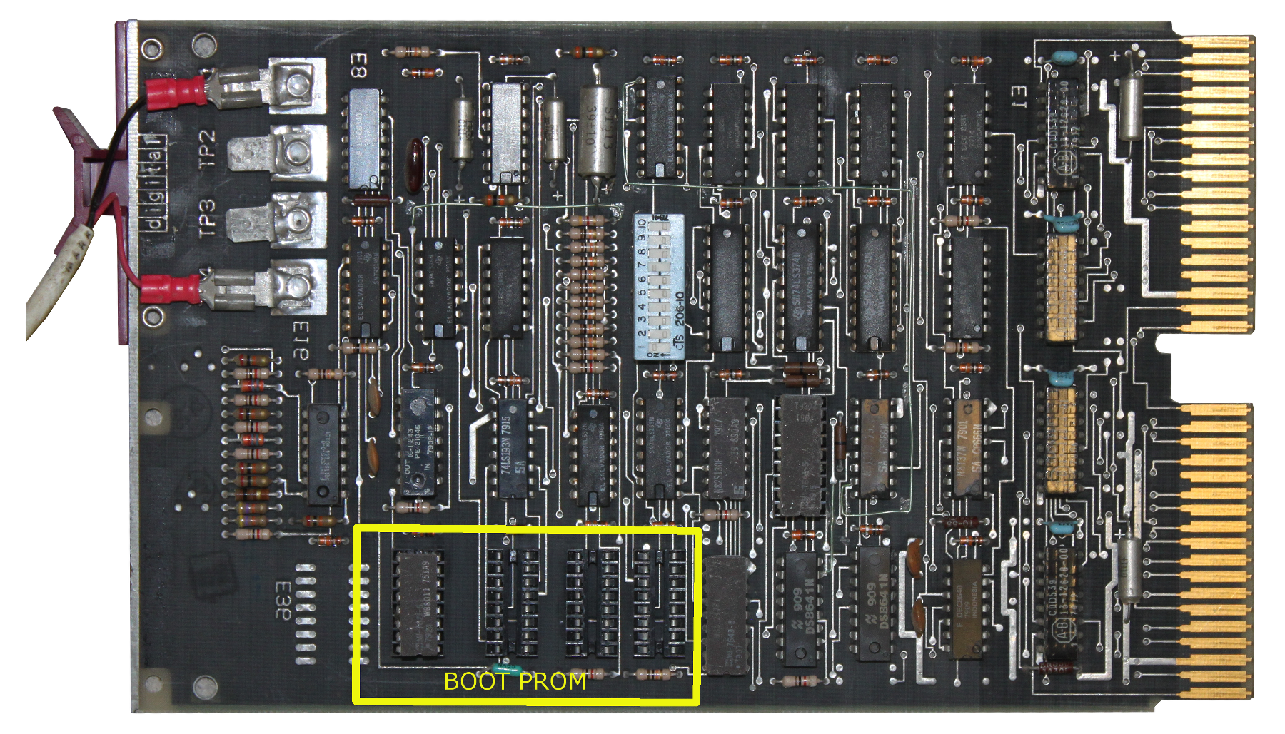
The last board, M9312, is used to boot the system, and also acts as a bus terminator. In general, the system must have two terminators, since the processor module itself does not perform this function. Therefore, another terminator must be installed on the opposite edge of the bus, in this case as close to the processor module as possible. The M9312 has four connectors for bipolar programmable ROMs, which provide support for booting from different devices. In addition, there is an EPROM on the board that contains the console emulator code for communication with the operator through the serial port.
The computer is screwed up in this document .
The first thing you need to start with is to check that everything is in order with the power supply. In particular, it is important to ensure that the capacitors are in good condition. H777 is a switching power supply with a key element in the secondary circuit, which implies that it contains a huge transformer ( compared to the circuit with the key in the primary circuit, it is really large ), which reduces the amplitude of the input AC voltage to much more pleasant 38 VAC. It is not very cool to mess with power supplies, in which voltage is in the region of 400 VDC in almost all sections of the circuit. H777 consists of two regulators: 5 volt, generating 25 amperes, and a MOS-regulator, giving + 15V, -15V, + 5V ( in other versions of H777 there is also a third regulator for + 20V, -5V ).
Some kind soul scanned the necessary manual , which describes in detail the entire internal kitchen of this PSU.
Large 50V x 22000mF capacitors filtering unregulated direct current were able to fully charge after 10k ohms, and the leakage current was extremely small. The 5V output capacitor was in much worse shape. The 6V x 3900mF capacitor from Sprague, on its impressive legs, has never reached its rated voltage, even when used for a long time with a 560 ohm resistor.
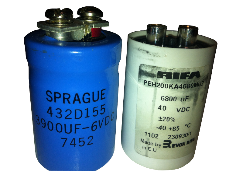
On the left is a time-damaged element, on the right is its replacement.
At present, such 6V x 3900mF capacitors with bolting cannot be found, so I replaced it with 40V x 6800mF from RIFA.
With the new capacitor, the PSU was able to deliver 3 amperes to my test board, from which a pleasant aroma of heated getinax soon stretched ( mock-ups are often made of this material ).
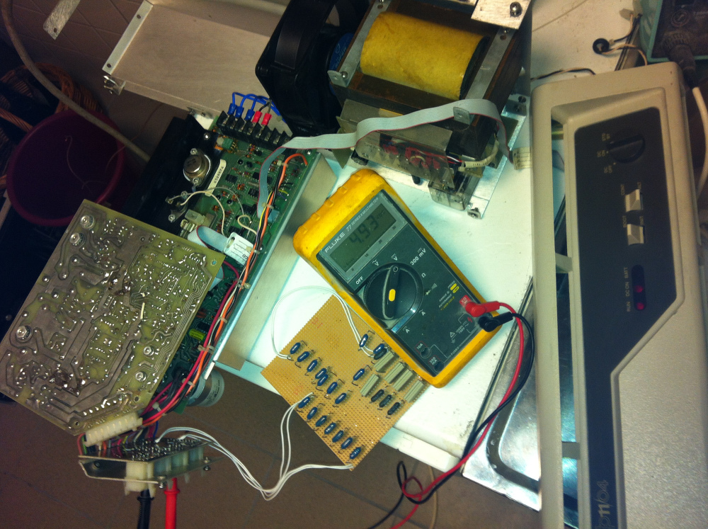
BP verification process. By the way, a healthy transformer of the primary circuit is visible.
But will all this work if you connect the PSU to the cross-board? Unfortunately, it did not work. It turned out that the two signal contacts of the PSU are in a permanently low state: BUS DC LO L and BUS AC LO L. These signals with an active low level and in the active state suppress the clock of the main processor.
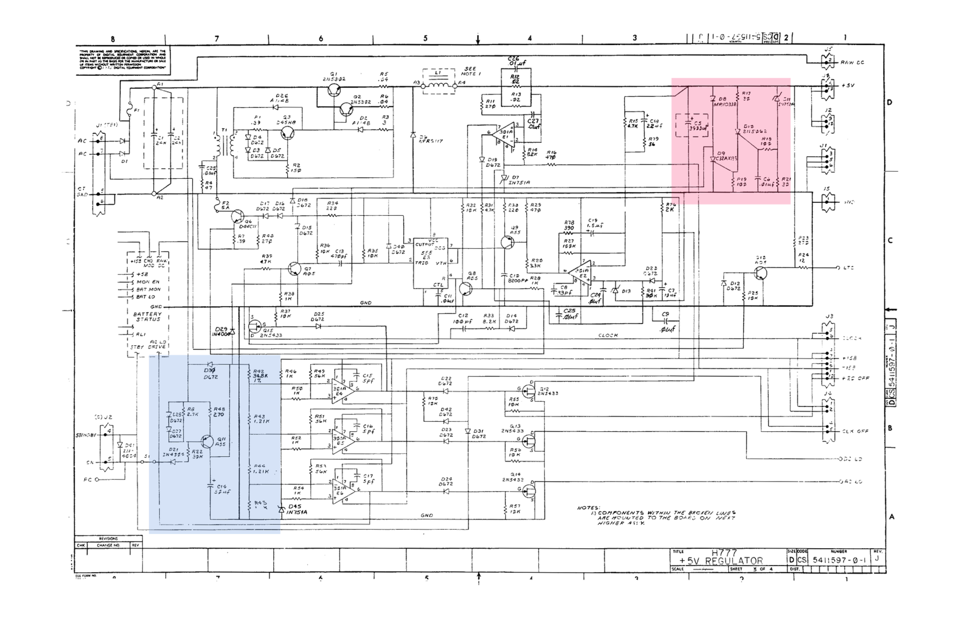
The circuit above describes a 5-volt regulator. The blue area is the current source circuit, which receives an unregulated constant current at the input, charging a 50mF capacitor, which then produces a beautiful sawtooth signal. Resistor matrix and a set of comparators ( operational amplifiers, which act here as voltage comparators) generate BUS DC LO L, BUS AC LO L and the internal signal on which the clock of the main PWM key is based. The voltage across the capacitor did not exceed 20.4 volts, which is not enough to change the polarity of the two comparators. It looked as if too much current was being absorbed from this source. Replacing the capacitor did not change anything. But, in addition to the current source, a red area of the circuit is connected to the capacitor - the overload protection circuit. If any of the transistor switches fails, then 38 volts of unregulated direct current will go to the output. Which, of course, is not very good. Therefore, a zener diode and a pair of thyristors are used here, which operate at an output voltage greater than 5.4 VDC, which leads to a short circuit in the current source, and, in turn, extremely effectively stops any activity in the power supply. The problem, apparently, was that, even under normal conditions, 1.5 mA was absorbed by the protective circuit due to thyristor leakage, moreover, in the closed state. Of course, any thyristor flows, but not as much as this one.
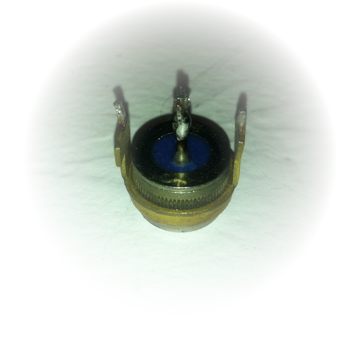
broken thyristor, possibly C32AX135
After replacing the thyristor with a modern BT145, the power supply has worked as it should.
We connect all the cables and turn on the power. Smoke is not visible, which is a good sign. But the “RUN” lamp often flickers, and, after switching the corresponding toggle switch on the console to the “INIT” value, it only blinked briefly once. The situation is not encouraging.
An oscilloscope connected to the main clock signal of the processor module shows that at the beginning there are 8 cycles, then a pause for a couple of microseconds, 3 cycles, another pause and again 3 cycles, but nothing follows after them.

In this photo you can see that the clock period is closer to 250 ns than to 260 ns, which are written about in Computer Engineering. However, the use of a delay line in the feedback circuit will not be able to give such accuracy. However, 4 MHz is a very impressive result for the mid-seventies.
Most likely, the oscilloscope could not help in further clarifying the causes of the problem. For these kinds of tasks, I keep this little USB analyzer.
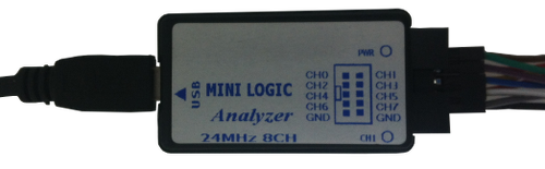
But in order to cover the entire computer with its address and data buses, I need four of these. Fortunately, at that moment I was offered to buy an HP1664A logic analyzer at an affordable price.
After some problems at the beginning, when I mixed up some signals and forgot that the board uses active-low levels, I got some interesting trace logs:
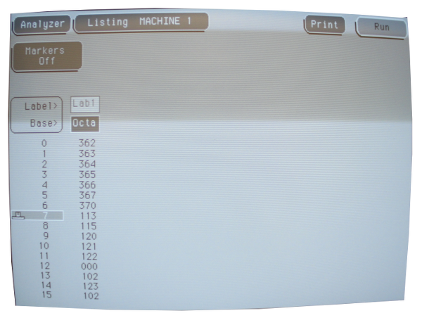
Here you can see the bus value along which the addresses of micro-instructions for execution are transmitted. In fact, the address of the next micro-instruction is shown here, while the current one is being executed. However, judging by the manual , this is a completely correct sequence of micro-operations ( if really interesting, then chapter 6.3.3 Restarts from power failure ).
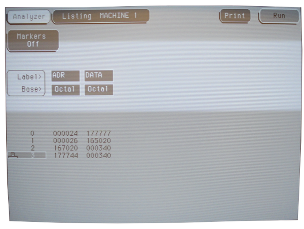
It’s interesting in the log above that when setting the address bus value to 026, we get 0165020, which is the value of the instruction counter containing the address from which we should start execution after a power failure. This address belongs to M9312 and indicates a diagnostic program. But the next instruction address set on the bus is 0167020. For some reason, the 10th bit turned out to be one! Studying in more detail the DS8641 bus receiver chip, I noticed that even with an input current of 3.31V, we get 3.78V at the output! It looks weird.
Here, this little malicious contraption:
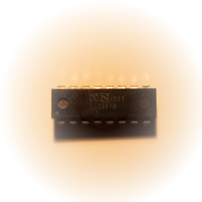
Unfortunately, the DS8641 is not a very common chip. In addition, it has been specially adapted for open collector buses for DEC. I ordered several on Ebay from a seller from China, but since the parcel has been going on for quite some time, I decided to drop the same chip from another board and replace it with a failed chip in the processor module.
This time the result was better:
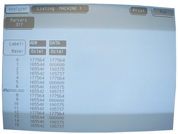
Nevertheless, it all ends with a looped wait for the TX readiness bit of the console serial port. It’s strange. Maybe the matter is the error M7800?
Another M7800 module was connected to the cross-board. The serial port is connected to a laptop.
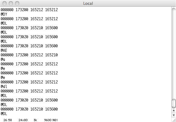
Excellent. Now the system goes through all the diagnostic steps from first to fourth. But entering “DL” in the console in order to try to boot from a non-existent RL device ( RL01 / RL02 is something like hard drives, but with removable data cartridges. ), Causes the machine to stop.

It seems that when you try to test the RAM, a crash occurs, and then, immediately, we get a double error during the processing of the first. This behavior is typical for exception handling ( more precisely, trap, trap ) by the processor.
While examining the memory module and checking jumpers and switch positions, I found that when I click the DIP switch back and forth, the position of the 6th key out of 8 is ignored, and the circuit remains closed. The problem.
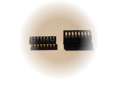
On the left is the new switch, on the right is the old one.
Finally, the computer started up!
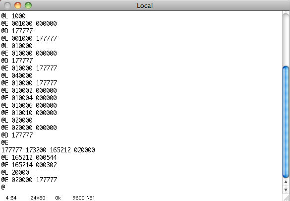
You can understand that it works by the fact that the author enters console commands in the terminal: @L - load the address, @E - check the data at the address, @D - write data at the loaded address .
PDP11GUI is a great Windows utility for managing your PDP-11. She is able to load files into the PDP-11 memory, view the memory cast and start the processor.
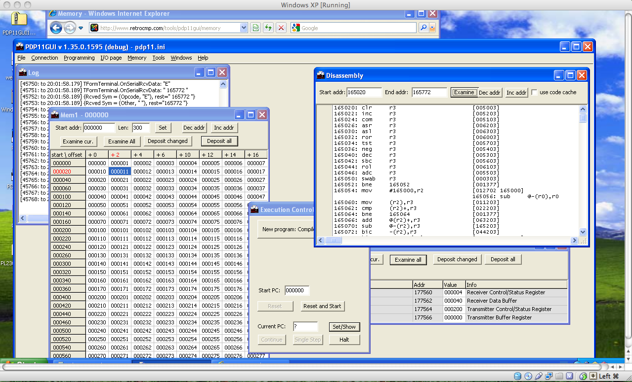
Punched tapes with BASIC can be found on the Internet. But, unfortunately, they are in Absolute Binary Loader format, which PDP11GUI does not understand. However, you can write a simple C program to convert. The resulting file can already be fed with a mini-computer, but it's all very slow on the 9600bps line.
UPDATE: In version 1.38 PDP11GUI no longer needs an external program, since the conversion code was included in PDP11GUI . ( Yes, in the original 5 identical references to PDP11GUI ).
Running PDP with the starting address 016104, we get BASIC's invitation ( it is obvious that the launch passed through the tool that has the corresponding “initial PC” setting ).
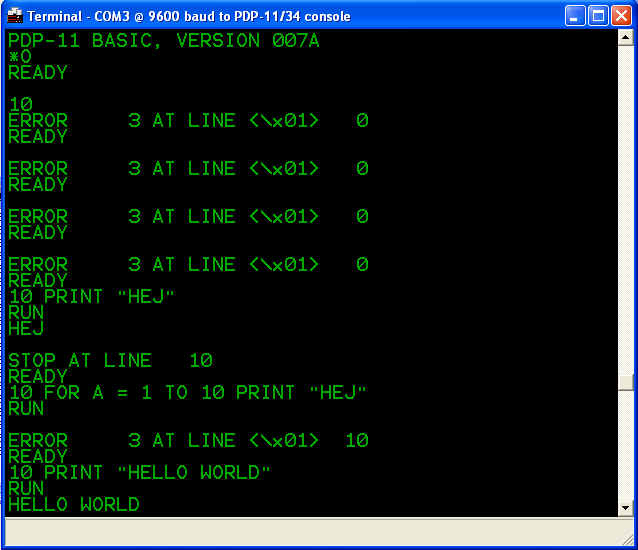
It is noticeable that I have not written anything in BASIC for a very long time.
For a real check that the processor works as it should, there are two diagnostic programs - GKAA and GKAB. There are two ways to run them: load a punched tape image into the PDP11GUI or use XXDP. I tried both methods.
It is well known that these programs were stored on punched tape, but, alas, I could not find images of these punched tapes. But I found an image for XXDP that contained GKAAA0.BIC and GKABC0.BIC. It turns out that binaries have the same format as punched tapes. I used PUTR to extract them from the image. Do not forget that you need to copy files as binary, and not just like me, you will rack your brains for several hours ( PUTR provides some DOS-like interface, and you need to do “copy / b” instead of just “copy” ).
After extracting, I just uploaded the images to PDP11GUI and started from address 0200.
XXDP must be started from some kind of storage device. Only one option is suitable for me, which would be simple enough for use on my PDP-11 at that moment - TU58 ( tape system ), since it uses a serial port for connection, and therefore can be emulated on a PC. I downloaded tu58em and compiled on my Mac. It was necessary to make only a few corrections in the code for working with the serial port in order for the program to compile successfully.
After that, I started working on creating a boot image with XXDP. This kind of work can be done much faster using the PDP-11 emulator. I used E11 . First I tried XXDP 2.6, found as an image on bitsavers:
But it required more memory than it was on my machine, so using this version would not work. In addition, GKAB did not want to run on the emulated PDP-11/04 for an unknown reason.
After that, I took the time to create a TU58 image for XXDP +, an earlier version of the XXDP package. Here's how I got it in E11:
GKAAA0.BIC under XXDP + on a real machine started successfully. Most of the system is in excellent condition! Here is a link to the image I made.
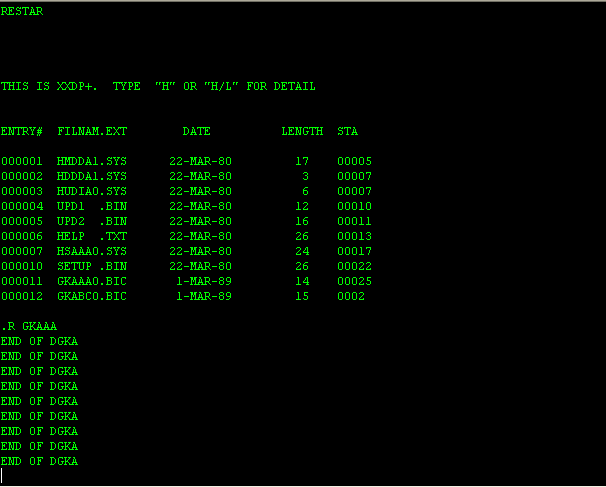
But starting GKABC0 ended with a system shutdown. It is not possible to find the source for a specific version of the utility, but the version for PDP-11/34 should work. Looking through the code , you can see that the part where the system is shutting down is checking the stack overflow processing logic. The stack pointer is set to 0400, and then the console TX interrupt is jerked ( apparently IOT instruction, which causes interrupt 020, on which the OS usually hangs the I / O handler) In this case, the stack pointer becomes less than 0400, which leads to an exception whose processing vector number is 4 or 6. On my machine, the behavior was different - more and more console interrupts were generated until the stack reached 0177774 (physical memory for this no address), and then stopped with a double bus error.
Changing the boards, I noticed that using another DL11-W fixes the problem. In DL11-W, the interrupt logic seems to be broken. The interrupt should be cleared as soon as the processor responds with SSYN ( Unibus bus signal, a kind of handshake ). This did not happen on a broken map. Only the processor began processing the interrupt, as it received it again and again. The process of working with interrupts on the Unibus bus is not very complicated. The device sets the BRn signal, and the processor responds with the BGn setting when it is ready for interrupt service. After that, the device, in turn, answers SACK, sets the number of the interrupt vector and pulls up the INTR. The trace below is taken from a working card:
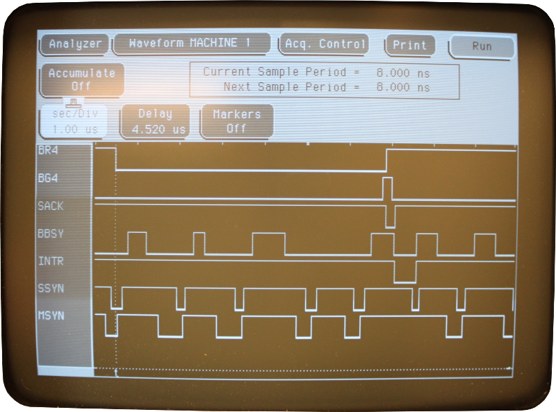
Do not forget that in the PDP-11 the active signal level is low
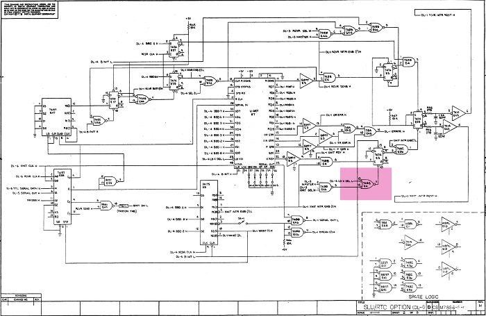
The circuit shows an interrupt trigger and a valve that should clear the interrupt signal when it is already in service.
This fuzzy photo clearly shows a failing 7408 AND-gate on a broken board.

7408 here is designated as E4, 12 and 13 are input signals, 11 is an output signal, which should, in theory, clear the interrupt when it is in a low state. This does not happen, and interruptions all go and go.
This completes the repair of the main unit board, in the second part of the article we fix the TU60 tape station, and in the third - the LA30 Decwriter terminal.
This PDP 11/04 was originally owned by Ericsson. We received it in the late eighties from EDKX - computer club Ericsson. The computer was handed over in parts, but everything was in place except for a couple of screws. Together with the PDP-11 itself was the TU60 tape station.
The
PDP-11/04 operator console panel appeared in the mid-seventies as the cheaper PDP-11/05 successor. In this new version, DEC was able to fit all the processor logic on one six-pin board (PDP used several types of boards with various form factors - six-pin, four-pin, two-pin. In the photo just below 6 groups of pins are visible. In addition, the boards were divided according to which bus they are designed for. ) instead of two in the predecessor. The modules were connected to a common cross-board ( backplate ) with nine slots performed by wrap-up. Typically, PDP 11 came with a programming console ( separate panel. PDP was assembled from several blocks. Something like a rack with a set of equipment ), through which the operator could enter simple boot programs and carry out system maintenance. However, this particular instance had only the usual limited operator console.
Cross Board
BookComputer Engineering: A DEC view of hardware design The PDP-11 family of machines is described in great detail. The book is scanned and is in the public domain. Very exciting reading!
CPU Board
The processor module consists of 138 chips. A slight simplification of the operational machine ( datapath, the part of the processor that performs operations on any data. For example, these are ALUs, multiplexers, register files, decoders. In general, this is practically the most important part of the processor.) and the use of programmable memory has reduced the number of chips used. The board has five 256x8 bipolar programmable ROM chips allocated for storing microcode, which is packed in 40-bit structures. The first eight bits are allocated to the address of the next microinstruction. An interesting feature is that the line along which these addresses are transmitted is implemented according to an open collector scheme, which allows conditional branching of microcode to be done simply using wired OR connections directly on the bus. As the main ALU, DEC took the well-known 74181, and Intel 3101 16x4 RAM chips were used as scratchpad memory for main registers. There is no separate crystal for clocking, but instead there is a delay line in the feedback circuit.
Memory
Card We got a PDP-11/04 with a 16 kilobyte memory module. It contains 32 MK4096, MOS dynamic memory chips produced by MOSTEK. An entertaining remark - this was the first memory with multi-addressing column / row addressing, a similar scheme is used in modern DDR. Thanks to this innovation, MOSTEK engineers were able to fit 4 kilobits of memory into a 16-pin package.
This is the M7800 card, DL11 asynchronous communications module. ( The PDP-11 used its own classification of modules. For example, the diagram indicates MS11-JP, which means a memory module, but specific boards could vary - M7867-XJ, M7847-DJ or some other card that complies with the module standard. In this case DL11 is a classifier, and the M7800 is a specific board. )
The last board, M9312, is used to boot the system, and also acts as a bus terminator. In general, the system must have two terminators, since the processor module itself does not perform this function. Therefore, another terminator must be installed on the opposite edge of the bus, in this case as close to the processor module as possible. The M9312 has four connectors for bipolar programmable ROMs, which provide support for booting from different devices. In addition, there is an EPROM on the board that contains the console emulator code for communication with the operator through the serial port.
The computer is screwed up in this document .
Checking the power supply H777
The first thing you need to start with is to check that everything is in order with the power supply. In particular, it is important to ensure that the capacitors are in good condition. H777 is a switching power supply with a key element in the secondary circuit, which implies that it contains a huge transformer ( compared to the circuit with the key in the primary circuit, it is really large ), which reduces the amplitude of the input AC voltage to much more pleasant 38 VAC. It is not very cool to mess with power supplies, in which voltage is in the region of 400 VDC in almost all sections of the circuit. H777 consists of two regulators: 5 volt, generating 25 amperes, and a MOS-regulator, giving + 15V, -15V, + 5V ( in other versions of H777 there is also a third regulator for + 20V, -5V ).
Some kind soul scanned the necessary manual , which describes in detail the entire internal kitchen of this PSU.
Large 50V x 22000mF capacitors filtering unregulated direct current were able to fully charge after 10k ohms, and the leakage current was extremely small. The 5V output capacitor was in much worse shape. The 6V x 3900mF capacitor from Sprague, on its impressive legs, has never reached its rated voltage, even when used for a long time with a 560 ohm resistor.
On the left is a time-damaged element, on the right is its replacement.
At present, such 6V x 3900mF capacitors with bolting cannot be found, so I replaced it with 40V x 6800mF from RIFA.
With the new capacitor, the PSU was able to deliver 3 amperes to my test board, from which a pleasant aroma of heated getinax soon stretched ( mock-ups are often made of this material ).
BP verification process. By the way, a healthy transformer of the primary circuit is visible.
But will all this work if you connect the PSU to the cross-board? Unfortunately, it did not work. It turned out that the two signal contacts of the PSU are in a permanently low state: BUS DC LO L and BUS AC LO L. These signals with an active low level and in the active state suppress the clock of the main processor.
The circuit above describes a 5-volt regulator. The blue area is the current source circuit, which receives an unregulated constant current at the input, charging a 50mF capacitor, which then produces a beautiful sawtooth signal. Resistor matrix and a set of comparators ( operational amplifiers, which act here as voltage comparators) generate BUS DC LO L, BUS AC LO L and the internal signal on which the clock of the main PWM key is based. The voltage across the capacitor did not exceed 20.4 volts, which is not enough to change the polarity of the two comparators. It looked as if too much current was being absorbed from this source. Replacing the capacitor did not change anything. But, in addition to the current source, a red area of the circuit is connected to the capacitor - the overload protection circuit. If any of the transistor switches fails, then 38 volts of unregulated direct current will go to the output. Which, of course, is not very good. Therefore, a zener diode and a pair of thyristors are used here, which operate at an output voltage greater than 5.4 VDC, which leads to a short circuit in the current source, and, in turn, extremely effectively stops any activity in the power supply. The problem, apparently, was that, even under normal conditions, 1.5 mA was absorbed by the protective circuit due to thyristor leakage, moreover, in the closed state. Of course, any thyristor flows, but not as much as this one.
broken thyristor, possibly C32AX135
After replacing the thyristor with a modern BT145, the power supply has worked as it should.
Processor check
We connect all the cables and turn on the power. Smoke is not visible, which is a good sign. But the “RUN” lamp often flickers, and, after switching the corresponding toggle switch on the console to the “INIT” value, it only blinked briefly once. The situation is not encouraging.
An oscilloscope connected to the main clock signal of the processor module shows that at the beginning there are 8 cycles, then a pause for a couple of microseconds, 3 cycles, another pause and again 3 cycles, but nothing follows after them.
In this photo you can see that the clock period is closer to 250 ns than to 260 ns, which are written about in Computer Engineering. However, the use of a delay line in the feedback circuit will not be able to give such accuracy. However, 4 MHz is a very impressive result for the mid-seventies.
Most likely, the oscilloscope could not help in further clarifying the causes of the problem. For these kinds of tasks, I keep this little USB analyzer.
But in order to cover the entire computer with its address and data buses, I need four of these. Fortunately, at that moment I was offered to buy an HP1664A logic analyzer at an affordable price.
Search for errors using a logic analyzer
After some problems at the beginning, when I mixed up some signals and forgot that the board uses active-low levels, I got some interesting trace logs:
Here you can see the bus value along which the addresses of micro-instructions for execution are transmitted. In fact, the address of the next micro-instruction is shown here, while the current one is being executed. However, judging by the manual , this is a completely correct sequence of micro-operations ( if really interesting, then chapter 6.3.3 Restarts from power failure ).
It’s interesting in the log above that when setting the address bus value to 026, we get 0165020, which is the value of the instruction counter containing the address from which we should start execution after a power failure. This address belongs to M9312 and indicates a diagnostic program. But the next instruction address set on the bus is 0167020. For some reason, the 10th bit turned out to be one! Studying in more detail the DS8641 bus receiver chip, I noticed that even with an input current of 3.31V, we get 3.78V at the output! It looks weird.
It's alive!
Here, this little malicious contraption:
Unfortunately, the DS8641 is not a very common chip. In addition, it has been specially adapted for open collector buses for DEC. I ordered several on Ebay from a seller from China, but since the parcel has been going on for quite some time, I decided to drop the same chip from another board and replace it with a failed chip in the processor module.
This time the result was better:
Nevertheless, it all ends with a looped wait for the TX readiness bit of the console serial port. It’s strange. Maybe the matter is the error M7800?
Another M7800 board
Another M7800 module was connected to the cross-board. The serial port is connected to a laptop.
Excellent. Now the system goes through all the diagnostic steps from first to fourth. But entering “DL” in the console in order to try to boot from a non-existent RL device ( RL01 / RL02 is something like hard drives, but with removable data cartridges. ), Causes the machine to stop.
It seems that when you try to test the RAM, a crash occurs, and then, immediately, we get a double error during the processing of the first. This behavior is typical for exception handling ( more precisely, trap, trap ) by the processor.
Clumsy DIP Switch!
While examining the memory module and checking jumpers and switch positions, I found that when I click the DIP switch back and forth, the position of the 6th key out of 8 is ignored, and the circuit remains closed. The problem.
On the left is the new switch, on the right is the old one.
Finally, the computer started up!
You can understand that it works by the fact that the author enters console commands in the terminal: @L - load the address, @E - check the data at the address, @D - write data at the loaded address .
PDP11GUI
PDP11GUI is a great Windows utility for managing your PDP-11. She is able to load files into the PDP-11 memory, view the memory cast and start the processor.
Punched tapes with BASIC can be found on the Internet. But, unfortunately, they are in Absolute Binary Loader format, which PDP11GUI does not understand. However, you can write a simple C program to convert. The resulting file can already be fed with a mini-computer, but it's all very slow on the 9600bps line.
Hidden text
#include
#include
int main (int argc, char ** argv) {
FILE * input, * output;
int ch, state = 0, count, size, sum = 0, address, data=0, start=0;
if (argc==3) {
input = fopen (argv[1], "rb");
if (input == NULL) {
fprintf(stderr, "cannot open file %s for reading\n", argv[1]);
exit(1);
}
output = fopen (argv[2], "w+");
if (output == NULL) {
fprintf(stderr, "cannot open file %s for reading\n", argv[2]);
exit(1);
}
}
else {
fprintf(stderr, "Usage conver UPDATE: In version 1.38 PDP11GUI no longer needs an external program, since the conversion code was included in PDP11GUI . ( Yes, in the original 5 identical references to PDP11GUI ).
Running PDP with the starting address 016104, we get BASIC's invitation ( it is obvious that the launch passed through the tool that has the corresponding “initial PC” setting ).
It is noticeable that I have not written anything in BASIC for a very long time.
Running diagnostics
For a real check that the processor works as it should, there are two diagnostic programs - GKAA and GKAB. There are two ways to run them: load a punched tape image into the PDP11GUI or use XXDP. I tried both methods.
It is well known that these programs were stored on punched tape, but, alas, I could not find images of these punched tapes. But I found an image for XXDP that contained GKAAA0.BIC and GKABC0.BIC. It turns out that binaries have the same format as punched tapes. I used PUTR to extract them from the image. Do not forget that you need to copy files as binary, and not just like me, you will rack your brains for several hours ( PUTR provides some DOS-like interface, and you need to do “copy / b” instead of just “copy” ).
After extracting, I just uploaded the images to PDP11GUI and started from address 0200.
Download XXDP
XXDP must be started from some kind of storage device. Only one option is suitable for me, which would be simple enough for use on my PDP-11 at that moment - TU58 ( tape system ), since it uses a serial port for connection, and therefore can be emulated on a PC. I downloaded tu58em and compiled on my Mac. It was necessary to make only a few corrections in the code for working with the serial port in order for the program to compile successfully.
After that, I started working on creating a boot image with XXDP. This kind of work can be done much faster using the PDP-11 emulator. I used E11 . First I tried XXDP 2.6, found as an image on bitsavers:
Hidden text
Ersatz-11 V7.0 Demo version, COMMERCIAL USE LIMITED TO 30-DAY EVALUATION
Copyright (C) 1993-2013 by Digby's Bitpile, Inc.  All rights reserved.
See www.dbit.com for more information.
E11>assign tt1: dda:
E11>mount dda0: dddp.dsk
E11>set cpu 04
E11>set mem 16
E11>boot tt1:
%HALT
?Bad kernel stack
R0/000000 R1/176506 R2/000000 R3/000066  CM=K PM=K PRIO=0
R4/100020 R5/000000 SP/057774 PC/000006  N=0 Z=0 V=0 C=0
000006  halt
E11>set mem 24
E11>boot tt1:
CPU NOT SUPPORTED BY XXDP-XM
BOOTING UP XXDP-SM SMALL MONITOR
XXDP-SM SMALL MONITOR - XXDP V2.6
REVISION: E0
BOOTED FROM DD0
12KW OF MEMORY
UNIBUS SYSTEM
RESTART ADDRESS: 052010
TYPE "H" FOR HELP
.R GKABC0
GKABC0.BIC
%HALT
R0/000357 R1/000000 R2/000300 R3/054426  CM=K PM=K PRIO=0
R4/000001 R5/000776 SP/000500 PC/012006  N=0 Z=0 V=0 C=0
012006  cmp     177776,#000000
E11>
But it required more memory than it was on my machine, so using this version would not work. In addition, GKAB did not want to run on the emulated PDP-11/04 for an unknown reason.
After that, I took the time to create a TU58 image for XXDP +, an earlier version of the XXDP package. Here's how I got it in E11:
Hidden text
.R UPD2
CHUP2A2 XXDP+ UPD2 UTILITY
RESTART: 002432
*ZERO DD0:
*DRIVER DD0:
*LOAD DY0:HMDDA1.SYS
XFR:005034  CORE:000000,017774
*SAVM DD0:
*PIP DD0:HMDDA1.SYS=DY0:HMDDA1.SYS
*PIP DD0:HDDDA1.SYS=DY0:HDDDA1.SYS
*PIP DD0:GKA???.BIC=DY0:GKA???.BIC
GKAAA0.BIC
GKABC0.BIC
*PIP DD0:HELP.TXT=DY0:HELP.TXT
*PIP DD0:HUDIA0.SYS=DY0:HUDIA0.SYS
*PIP DD0:HSAAA0.SYS=DY0:HSAAA0.SYS
*PIP DD0:UPD?.BIN=DY0:UPD?.BIN
UPD1  .BIN
UPD2  .BIN
*PIP DD0:SETUP.BIN=DY0:SETUP.BIN
E11>set cpu 04
E11>set mem 16
E11>boot tt1:
CLEARING MEMORY
CHMDDA0 XXDP+ DD MONITOR  8K
BOOTED VIA UNIT 0
ENTER DATE (DD-MMM-YY):
RESTART ADDR:033726
50 HZ? N   Y
LSI?   N
THIS IS XXDP+.  TYPE  "H" OR "H/L" FOR DETAILS
.DIR
ENTRY#  FILNAM.EXT        DATE          LENGTH  START
000001  HMDDA1.SYS      22-MAR-80         17    000050
000002  HDDDA1.SYS      22-MAR-80          3    000071
000003  GKAAA0.BIC      11-AUG-76         15    000074
000004  GKABC0.BIC      29-JAN-77         16    000113
000005  HELP  .TXT      22-MAR-80         26    000133
000006  HUDIA0.SYS      22-MAR-80          6    000165
000007  HSAAA0.SYS      22-MAR-80         24    000173
000010  UPD1  .BIN      22-MAR-80         12    000223
000011  UPD2  .BIN      22-MAR-80         16    000237
000012  SETUP .BIN      22-MAR-80         26    000257
.R GKABC0
%HALT
R0/000357 R1/000000 R2/000300 R3/032240  CM=K PM=K PRIO=0
R4/000001 R5/000776 SP/000500 PC/012006  N=0 Z=0 V=0 C=0
012006    cmp       177776,#000000
GKAAA0.BIC under XXDP + on a real machine started successfully. Most of the system is in excellent condition! Here is a link to the image I made.
But starting GKABC0 ended with a system shutdown. It is not possible to find the source for a specific version of the utility, but the version for PDP-11/34 should work. Looking through the code , you can see that the part where the system is shutting down is checking the stack overflow processing logic. The stack pointer is set to 0400, and then the console TX interrupt is jerked ( apparently IOT instruction, which causes interrupt 020, on which the OS usually hangs the I / O handler) In this case, the stack pointer becomes less than 0400, which leads to an exception whose processing vector number is 4 or 6. On my machine, the behavior was different - more and more console interrupts were generated until the stack reached 0177774 (physical memory for this no address), and then stopped with a double bus error.
Glitchy DL11-W!
Changing the boards, I noticed that using another DL11-W fixes the problem. In DL11-W, the interrupt logic seems to be broken. The interrupt should be cleared as soon as the processor responds with SSYN ( Unibus bus signal, a kind of handshake ). This did not happen on a broken map. Only the processor began processing the interrupt, as it received it again and again. The process of working with interrupts on the Unibus bus is not very complicated. The device sets the BRn signal, and the processor responds with the BGn setting when it is ready for interrupt service. After that, the device, in turn, answers SACK, sets the number of the interrupt vector and pulls up the INTR. The trace below is taken from a working card:
Do not forget that in the PDP-11 the active signal level is low
The circuit shows an interrupt trigger and a valve that should clear the interrupt signal when it is already in service.
This fuzzy photo clearly shows a failing 7408 AND-gate on a broken board.
7408 here is designated as E4, 12 and 13 are input signals, 11 is an output signal, which should, in theory, clear the interrupt when it is in a low state. This does not happen, and interruptions all go and go.
This completes the repair of the main unit board, in the second part of the article we fix the TU60 tape station, and in the third - the LA30 Decwriter terminal.