SimBank or 200 SmartCard in one box
As I already wrote in my first topic on Habré about the creation of a printed circuit board, my company is developing devices for telephony of various kinds of VoIP-, GSM-, PBX-gateways, socket-rebooters controlled via GSM and so on. Today I will describe the process of developing firmware for a SimBank device in its PCI version, where I acted as a developer of a circuit for FPGAs.
SimBank device is designed to work with SIM cards (Subscriber Identification Module - Subscriber Identity Module). These cards are a type of ISO-7816 card. It can be used for centralized storage of SIM cards or other types of smart-cards, and their subsequent use in devices such as a GSM gateway, satellite TV tuners or in other devices using smart-cards during operation. Together with the software, the Sim-server provides a flexible system for monitoring and accounting for SIM cards used in your applications, and extensive options for setting up and configuring the system through a convenient web-based interface. At the same time, the cards themselves are stored in an accessible place for you and are connected to terminal devices via TCP / IP protocol.
Habré has articles describing the device and operation of the smart cards:
A brief introduction to the SIM-card from OgreSwamp
Smart cards for the youngest of the brake
How does the smart card from rlepricon
I have them all happy to read before starting to develop. And I will not repeat what is written in them.

SimBank device
The device itself was made at the company for a long time and has been successfully used for several years. But the peculiarity of all PCI devices at the company was the training PCI core, "which was delivered as is and claims were not accepted." They were not exhibited. With minimal alterations, this core was put on all boards without exception. This allowed us to skillfully use the available address space. With the same Vendor ID, Device ID, Class Code. Since the devices are usually assembled at the company and checked for operability, there were no conflicts. In a limited time frame, the principle of “work - do not touch” is quite appropriate. This continued until for some time until some modern motherboards began to show instability in the work or in general the board did not want to start.
The time has come to deal more thoroughly with the PCI core. The training core modified for its tasks was documented by comments, but they were not always enough. The reference to the place from where it was taken, dated 2002 or 2004, did not work.
The task is as simple as a day: “The device should work on all standard boards.”
As a bonus: “Even if it will not be all 200 SIM cards, but 196 or 1xx.”
Until that moment, I had never worked with either SIM cards or the PCI bus as an FPGA developer. Only circuit and board. Development experience on VHDL and Verilog already was.
It was decided to start disassembling with PCI, as part related to SIM cards worked.
The first reading of the “PCI Local Bus” specification did not work miraculously and did not shed much light on how everything should be done. Having read the articles on how to do and how not to do it, I really didn’t understand anything yet, I decided: “I need to do, I’ll figure it out along the way”.
For PCI, Altera in Quartus has a Megafunction that allows you to generate a PCI core with the parameters we need. Good documentation is attached to the kernel, the site has a description of the PCI kit, to which the PCI model is attached, for behavioral modeling in ModelsSim-Altera. All this together - it helps a lot to get used to it from scratch in this thread. Altera
also allows you to use your Vendor ID (1172h).
In the PCI specification, a device class not available in the earlier versions of the specifications was selected: 07h - Simple Communication Controllers, 05h-Smart Card.
Next, everything should work on Linux. Since the colleague has more experience with both SIM cards and PCI, then he has technical requirements. For which many thanks to him. Properly written document is half the battle. Although it requires "extra scribbling."
Since the device was not developed by me, I also needed to get acquainted with the draft circuit and board.
The circuit part is necessary for understanding what is coming from and what it is connected to, and the board makes it clear where to insert the programmer, SIM card and where this or that service indication is located. About how it played a cruel joke with me, I will describe a little later.

According to the scheme, we have a board with two Altera Cyclone II EP2C35672C8 FPGAs in a case with 672 contacts. One FPGA is connected to the PCI bus and it also controls the second FPGA. Each FPGA has 100 SIM card holders attached. Each SIM card has its own reset and data signal, the CLK signal goes to a group of 10 cards.

Each EP2C35 chip contains 105 M4K internal memory blocks. In total, the RAM block (including the parity bit) has 4.608 bits.
Blocks support different configurations from 4K × 1 to 128 × 32 (36).
After that, I already wrote a document with additional questions, what will be submitted for, who is monitoring the duration of certain signals. Who considers the correctness of the arrival of data from the SIM and so on.
Having dealt with the contacts of the first microcircuit from the PCI bus, I made a trial project of the PCI core in Quartus, which was supposed to work with the new parameters on the bus. Without any logic - just the core.
Having received the answer to the “lspci -vv” command, my happiness knew no bounds.
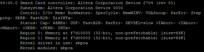
After discussing with the developer of the driver and the application program the further course of work, we made a pilot project in which the driver recorded data in memory, and then read and verified them. Initially, the check was done only on the first chip in the circuit.
Next was the analysis with the second microcircuit.
There are 36 signal lines + 2 lines between the PLL_OUT and CLK outputs between the two microcircuits in the circuit. In the previous project, 19 address lines and two bytes for data exchange (one in each direction) were used for reading signals and a writing signal. This was done based on the specifics of the existing kernel. And for universal driver and software. For example, there is a well-established part of the addresses from where service information can be subtracted.
Information is stored in ARM springs such as

Elgato G4_1 - device type (for PCI boards “K16” or “K32”, for Simbank - “SimBank”)
SIM51215 (SIM900 or another) - type of installed GSM or 3G module (required to select a set of AT commands). In relation to the described device, in terms of which SIM card we can get through this module to the operator’s network.
2014 - development year
ver.14.144 - version number of the
SN firmware : 0123
And if you didn’t forget to change it to the correct one before the firmware, then from this data you can find out a lot of interesting things from the “barn book”, where it was written under whom the project was made and what are the differences from the standard desired by the customer.
For Simbank, a serial number is enough. Since structurally, the Simbank board is always one in the device. And in the PCI version, there is only one such board in the company.
In the previous kernel version, two BARs were used. BAR1 with memory mapping of 1M, BAR0 as 4K input / output registers. All address space was given for both FPGAs simultaneously.
It was decided to abandon the use of IO for various reasons. First, the driver developer is much easier to work with memory. Secondly, the network has many recommendations why, if possible, it is worth abandoning IO in new developments. Thirdly, the amount of IO resources available for configuration in the core from Altera is limited to 256. There are much more memory resources that can be allocated. But this transition entailed a change in the work with SIM card modules. And it meant an almost complete alteration of the SIM exchange module. Moreover, the departure from the usual addressing meant that we could not read any bits we needed in any of our programs in the usual place.
It was possible not to do at two base addresses and do one. Do not save one clock signal when exchanging with cards of the first chip. This part of the data exchange is not involved in voice transmission and we do not need to save milliseconds in order to get a delay of no more than 20 ms. But that seemed right to me.
After the first successes and verification of writing test data to the memory, it was time to build a structure for exchanging data with SIM cards. I had a rough idea of how to do it for a long time, but after the tests I was ready to assume that it would work. And the tests done were thought out and done not in vain.
The existing 36 + 2 signal lines were not enough to translate the PCI bus service signals to the second chip without changes, and I did not want to limit the reception - transmission by one or two bytes. Even if you manage to span the address and data bus.
Therefore, 32 of the 36 signal lines were immediately sent to the data bus (and addresses), 1 signal line controlled the general reset of the system, and for the remaining three we walk and hang up all the controls. To transmit the CLK signal, we had a separate line.
Silence mode, address transfer mode, single data recording mode, streaming data recording (Burst), mask recording modes, reading and streaming reading. Only eight bus states that fit into three signal lines.
It remains only to transmit four BE signals for recording by mask. It was decided to hide them in the upper four bits on the data bus if we use this mode.
For each SIM card in the FPGA, the maximum possible buffer was allocated. Since a single-wire half-duplex interface is implemented with a Smart card, we have 100 cards, and there are only 105 memory cells in the microcircuit, it was decided to make a buffer for reception and transmission. And reset the addressing at the beginning of the transmission or reception. I was lucky and according to the standard, more than 256 bytes of data per command cannot come from a SIM card. So the available buffer will not overflow until we subtract it.
The term “team” here is slightly different from the ISO-7816 standard. There, under the command is meant access to the card, then confirmation from the card, and then data. But I'm interested in the amount of data from zeroing to zeroing the buffer.
It was decided not to make a buffer for exchanging data with the second microcircuit, but to write directly to the memory for SIM cards in the second microcircuit. Since I have already taken 102 memory blocks out of 105. The choice of the first and second microcircuit is selected through access to BAR0 or BAR1, respectively.
Different controllers are made for BAR0 and BAR1. The second microcircuit is accessed one cycle later, but this is regulated by the delay of the TRDY signal on the PCI bus side.
For each chip, 64K of memory is allocated, which is enough to serve 128 Smart cards. We have 100. There are still 28 blocks left. In two blocks we will place the service information where information about the status of the card reset and the exchange rate will be stored. Back we need to return the amount of received data from the SIM.
Then all this needs to be made to work and debug. Since the project for 100 SIM cards compiles for a very long time, and 100 SIM cards are much more expensive to burn than 1 or 10, it was decided to debug the exchange immediately on 1 - 5 cards, and then add all the rest. And to debug only the first half, and when we decide that everything worked out, we go to the second chip.
And then a surprise awaited me.
There is a scheme on which the card contacts are numbered from 1 to 100. There is a board project from which the FPGA contact settings are successfully imported (PCI works, test writing to memory works, exchange between microcircuits also works). The project is compiled for 5 cards, so if I make a mistake with the start of numbering from 0 or 1, then the second card would work. Pipes.
Well, nothing, we have 10 LEDs on the board. And although I was going to deal with them later, I had to later push a little closer to now. Add a simple thing to turn on / off the LED, and thelight is off, the LED does not blink.
We take an oscilloscope. CLOCK is, but there is no reset. No data either.
Import data failed? We compare the circuit with the board, the board and the circuit with Pin Planner in Quartus. Match up. But there is no reset.
And here the senior comrade comes to my aid. And he says that the“princess in another castle” in the “SIM0” program is on the other side of the box. And that has always been so.
Here you can take a screenshot of a piece from the PCB project in P-CAD. There are signatures of signals
On the board it is SIM 199, and in the project SIM0. The project is compiled for only 5 cards. (For 100, he just does not fit yet). And so the remaining 95 cards are simply not served. And for them, even the memory buffer in the FPGA is not formed.
In order to save resources, it was decided to clock the memory blocks with the frequency at which the SIM cards work. So fewer dividers will be needed. And with a lower frequency, it will be easier to get into the high-speed resources of the chip. It was planned to write to the buffer for the SIM card at the PCI bus speed (33 MHz), and read at the speed of work with SIM cards. Due to limitations on dual-port memory implementation, Cyclone II had to look for other solutions. As a result, it turned out to be the simplest and most correct to clock all 33 MHz blocks from PCI_CLK. And the decrease in the number of multi-bit counters had to be done by means of enable signals for clock registers. In addition, this approach made it easier to write time constraints for TimingAnalyzer using multycycle.
Model customization. For the successful completion of all inventions, we need a model. For the PCI core, the model is provided by Altera. For Smart cards, I had to write a model myself.
The downside of this solution, if I misunderstand how the SIM card should work, then I will also write the model incorrectly. But nothing happened. True, not right away.
The simulation allowed not to distract the colleague on the first couple, although later on we had to deal with the hardware at the debugging stage. What is wrong with the model, and how it should be.
Initially, work on resetting and reading from the ATR SIM card, changing the speed and sending a simple command “A0 A4 00 00 02” was debugged in the SIM card slot machine, and all this had to be answered “A4”. I wanted to make an automatic machine that would turn on everything myself upon turning on the power and, by the time the OS boots up, work with the SIM card at its maximum speed. This would allow to unload the program from the initialization of two hundred (200!) SIM cards during start.
With some SIM cards everything went fine, and some stubbornly gave away h'3B and were silent. As a result, the timer worked in the machine and I reset the SIM card. Since she did not tell me at what speed you can talk to her. If I received three or more than three bytes, then I thought that the ATR was read and you can continue to work. Although everything was wonderful on the model, but as it turned out, different SIM cards give ATR differently. Some give all the information at once, while others, after sending the h'3B header, there is a pause, and then all the information is displayed. Increasing the pause solved this problem. For the time being. Some SIM cards give the final bit with the same big pause as at the beginning after the byte h'3B.
It is resolved. No smart machines, spontaneous speed changes, and more. Let the processor think about it. He makes a decision when to issue a reset, remove it, and let him consider when a piece of data from the card is completed.
But there is a problem. We have not configured all the buns yet, and we have only 80-85 SIM cards out of the required 100 in each chip. Let the operating system driver do this. It’s not difficult for him, but it’s more spacious for us.
Next went debugging work with other commands already received from the driver from the OS. Debugging on a large number of SIM cards. And new “discoveries”.
How to decide if 197 out of 200 cards work, but three do not, is this the exact job or not? Testing was carried out on SIM cards blocked by the operator, which still responded to the reset and pretended to write SMS messages to themselves. Maybe three cards are locked for good reason and are they mistaken? I was so naive.
The very first work in real mode showed that everything was right on their part. Seek.
And I found. Not right away. My colleague who organized the exchange logs for all SIM cards helped. it turned out that sometimes when recording large teams my counter jumped. And I wrote one byte twice in the middle of a long transmission. Since behavioral modeling is a long business, I did not use long commands in the model. Limited to short transactions. He made truncated sizes of counters. He took a step, simulated, checked, earned. A little “Hurray!” And continue. We wrote down the byte, word, double word. A couple of addresses have passed - and then everything will be fine.
And now, on a small model, everything is fine, but in life it does not work. In this case, before the error, the SIM card manages to give your number (if it is recorded in the card), ICCID, IMSI and something else. And when simulating writing / reading to a SIM card. Not always, only three out of two hundred cards make mistakes.
Manual comparison of the program log and the logical analyzer showed that an error occurs in the body of the SMS message. At the same time, 197 cards let this error through the fingers count CRC. Why bother with some kind of SMS, and three cards still wait for their finest hour.
I finalized the model launched, and again everything is in order on it. How so?
I run the model with a complete check of the counters (Divide 33 MHz by 6, then by 372, and then again and again, instead of conditionally divide by 4, and then another by 16). The model launches in the evening, hoping to see everything in the morning ...
And in the morning we catch our OS sleeping, childish sleep. She turned off the screen in power saving mode. But we didn’t get to sleep with her. After 4+ hours of modeling more than 300 signals and buses, she fell asleep “without taking off her shoes”. And in the morning started up the third time. What a joy it is that I did not have to restore the entire system.
Day work, sleep shutdown. And the very next morning I could find a mistake. The truth before this all day I went to a showdown with all sorts of other tricks. And in the morning of a happy day, I already wondered where to look for a mistake.
It was not the last, there were other errors that were more obvious and easier in terms of production.
Having made the assumption that the work with the Smart Card is stable, I connected the second chip. First in the project. Then on the model. Then in iron. Not all at once, but we overcame this part. How to check that all 200 seats work simultaneously and do not interfere with neighbors? Where to get so many SIM cards? Found 200 pieces on the gimbal. Launched.
They started, they gave the bank for verification. And here is another surprise. If all places are occupied in SimBank, then everything is fine. Cards work stably, they are not often discarded. And if some of the cards are not installed, then a periodic reset comes in their place. But sometimes the reset comes on the symmetric cards of the neighboring FPGA. Why?
I still don’t really know the answer to this question. But now I know what Signal Tap II Logic Analyzer is in Altera's Quartus. Using it, it was possible through JTAG to pull out the signal states on the PCI bus. By changing the project and creating new signals to start the countdown or stop, it was possible to view some parts inside the FPGA. So for example, I was surprised to learn that when reading or writing more than eight bytes, Burst mode almost never turns on. By record, never, and when reading no more than two PCI cycles. Although the command “read 40 bytes” comes from the program, and reading takes four bytes each. From setting the address to PCI, the

problem of discharges was partially solved by the driver on the software side. Partially, the restriction did not use the odd number of SIM cards in the bank until better times.
Question to the audience: is there a possibility in Linux (Centos 6 32-bit) to write all the access logs to the device? It is advisable not to interfere with the operation of the PCI bus. So that you can set the Vendor ID / Device ID and save its R / W access logs on the bus?
As a result, by the end of all improvements, a full FPGA project consumes 89% of logic elements and 85% of available internal memory. Everything fit, and this means that the elementary base and structure of the project are chosen correctly.
According to the scheme, two 50 MHz oscillators are saved, since the project takes only a 33 MHz PCI clock signal, they are not used and may not be installed on the board in the future. The project works with all motherboards “slipped” today.
The device can register all cards on the network at once, if only GSM channels are enough.
Now, in addition to updating firmware and drivers for customers, several devices are working with us. Some send SMS for SprintSMS project. Others are “protected” by our technical support and work for the benefit of the customer. This made it possible to understand the essence of the customer’s work, and what he really needed. Both in terms of ergonomics and in terms of additional software functionality. In addition, a stably working device (knock-knock-knock so as not to jinx it) made it possible to better debug software.

But that's another story.
Thanks to all.
Readers for their interest in the article. To authors of other articles - for useful lessons. To creators of Habr for Habr. Colleagues for help in difficult times and “provided” experience. To the leader - for understanding.
PS As a bonus, a picture from the web-based interface of visual control over the work of SimBank.
Special thanks to him for Maxim.

Here SimBank is launched in a mode of 100 cards.

List of cards with deducted information from them. On cards that require a PIN, part of the information is not available.

The web interface is also available from smartphones.
Yellow cards that are currently in operation are highlighted.
History of the problem statement from the management + device operation history
SimBank device is designed to work with SIM cards (Subscriber Identification Module - Subscriber Identity Module). These cards are a type of ISO-7816 card. It can be used for centralized storage of SIM cards or other types of smart-cards, and their subsequent use in devices such as a GSM gateway, satellite TV tuners or in other devices using smart-cards during operation. Together with the software, the Sim-server provides a flexible system for monitoring and accounting for SIM cards used in your applications, and extensive options for setting up and configuring the system through a convenient web-based interface. At the same time, the cards themselves are stored in an accessible place for you and are connected to terminal devices via TCP / IP protocol.
Habré has articles describing the device and operation of the smart cards:
A brief introduction to the SIM-card from OgreSwamp
Smart cards for the youngest of the brake
How does the smart card from rlepricon
I have them all happy to read before starting to develop. And I will not repeat what is written in them.
SimBank device
The device itself was made at the company for a long time and has been successfully used for several years. But the peculiarity of all PCI devices at the company was the training PCI core, "which was delivered as is and claims were not accepted." They were not exhibited. With minimal alterations, this core was put on all boards without exception. This allowed us to skillfully use the available address space. With the same Vendor ID, Device ID, Class Code. Since the devices are usually assembled at the company and checked for operability, there were no conflicts. In a limited time frame, the principle of “work - do not touch” is quite appropriate. This continued until for some time until some modern motherboards began to show instability in the work or in general the board did not want to start.
The time has come to deal more thoroughly with the PCI core. The training core modified for its tasks was documented by comments, but they were not always enough. The reference to the place from where it was taken, dated 2002 or 2004, did not work.
The task is as simple as a day: “The device should work on all standard boards.”
As a bonus: “Even if it will not be all 200 SIM cards, but 196 or 1xx.”
Until that moment, I had never worked with either SIM cards or the PCI bus as an FPGA developer. Only circuit and board. Development experience on VHDL and Verilog already was.
It was decided to start disassembling with PCI, as part related to SIM cards worked.
The first reading of the “PCI Local Bus” specification did not work miraculously and did not shed much light on how everything should be done. Having read the articles on how to do and how not to do it, I really didn’t understand anything yet, I decided: “I need to do, I’ll figure it out along the way”.
For PCI, Altera in Quartus has a Megafunction that allows you to generate a PCI core with the parameters we need. Good documentation is attached to the kernel, the site has a description of the PCI kit, to which the PCI model is attached, for behavioral modeling in ModelsSim-Altera. All this together - it helps a lot to get used to it from scratch in this thread. Altera
also allows you to use your Vendor ID (1172h).
In the PCI specification, a device class not available in the earlier versions of the specifications was selected: 07h - Simple Communication Controllers, 05h-Smart Card.
Next, everything should work on Linux. Since the colleague has more experience with both SIM cards and PCI, then he has technical requirements. For which many thanks to him. Properly written document is half the battle. Although it requires "extra scribbling."
Material study
Since the device was not developed by me, I also needed to get acquainted with the draft circuit and board.
The circuit part is necessary for understanding what is coming from and what it is connected to, and the board makes it clear where to insert the programmer, SIM card and where this or that service indication is located. About how it played a cruel joke with me, I will describe a little later.
According to the scheme, we have a board with two Altera Cyclone II EP2C35672C8 FPGAs in a case with 672 contacts. One FPGA is connected to the PCI bus and it also controls the second FPGA. Each FPGA has 100 SIM card holders attached. Each SIM card has its own reset and data signal, the CLK signal goes to a group of 10 cards.
Each EP2C35 chip contains 105 M4K internal memory blocks. In total, the RAM block (including the parity bit) has 4.608 bits.
Blocks support different configurations from 4K × 1 to 128 × 32 (36).
After that, I already wrote a document with additional questions, what will be submitted for, who is monitoring the duration of certain signals. Who considers the correctness of the arrival of data from the SIM and so on.
Having dealt with the contacts of the first microcircuit from the PCI bus, I made a trial project of the PCI core in Quartus, which was supposed to work with the new parameters on the bus. Without any logic - just the core.
Having received the answer to the “lspci -vv” command, my happiness knew no bounds.
After discussing with the developer of the driver and the application program the further course of work, we made a pilot project in which the driver recorded data in memory, and then read and verified them. Initially, the check was done only on the first chip in the circuit.
Next was the analysis with the second microcircuit.
There are 36 signal lines + 2 lines between the PLL_OUT and CLK outputs between the two microcircuits in the circuit. In the previous project, 19 address lines and two bytes for data exchange (one in each direction) were used for reading signals and a writing signal. This was done based on the specifics of the existing kernel. And for universal driver and software. For example, there is a well-established part of the addresses from where service information can be subtracted.
Information is stored in ARM springs such as
Elgato G4_1 - device type (for PCI boards “K16” or “K32”, for Simbank - “SimBank”)
SIM51215 (SIM900 or another) - type of installed GSM or 3G module (required to select a set of AT commands). In relation to the described device, in terms of which SIM card we can get through this module to the operator’s network.
2014 - development year
ver.14.144 - version number of the
SN firmware : 0123
And if you didn’t forget to change it to the correct one before the firmware, then from this data you can find out a lot of interesting things from the “barn book”, where it was written under whom the project was made and what are the differences from the standard desired by the customer.
For Simbank, a serial number is enough. Since structurally, the Simbank board is always one in the device. And in the PCI version, there is only one such board in the company.
Painful decision
In the previous kernel version, two BARs were used. BAR1 with memory mapping of 1M, BAR0 as 4K input / output registers. All address space was given for both FPGAs simultaneously.
It was decided to abandon the use of IO for various reasons. First, the driver developer is much easier to work with memory. Secondly, the network has many recommendations why, if possible, it is worth abandoning IO in new developments. Thirdly, the amount of IO resources available for configuration in the core from Altera is limited to 256. There are much more memory resources that can be allocated. But this transition entailed a change in the work with SIM card modules. And it meant an almost complete alteration of the SIM exchange module. Moreover, the departure from the usual addressing meant that we could not read any bits we needed in any of our programs in the usual place.
It was possible not to do at two base addresses and do one. Do not save one clock signal when exchanging with cards of the first chip. This part of the data exchange is not involved in voice transmission and we do not need to save milliseconds in order to get a delay of no more than 20 ms. But that seemed right to me.
Structure
After the first successes and verification of writing test data to the memory, it was time to build a structure for exchanging data with SIM cards. I had a rough idea of how to do it for a long time, but after the tests I was ready to assume that it would work. And the tests done were thought out and done not in vain.
The existing 36 + 2 signal lines were not enough to translate the PCI bus service signals to the second chip without changes, and I did not want to limit the reception - transmission by one or two bytes. Even if you manage to span the address and data bus.
Therefore, 32 of the 36 signal lines were immediately sent to the data bus (and addresses), 1 signal line controlled the general reset of the system, and for the remaining three we walk and hang up all the controls. To transmit the CLK signal, we had a separate line.
Silence mode, address transfer mode, single data recording mode, streaming data recording (Burst), mask recording modes, reading and streaming reading. Only eight bus states that fit into three signal lines.
It remains only to transmit four BE signals for recording by mask. It was decided to hide them in the upper four bits on the data bus if we use this mode.
For each SIM card in the FPGA, the maximum possible buffer was allocated. Since a single-wire half-duplex interface is implemented with a Smart card, we have 100 cards, and there are only 105 memory cells in the microcircuit, it was decided to make a buffer for reception and transmission. And reset the addressing at the beginning of the transmission or reception. I was lucky and according to the standard, more than 256 bytes of data per command cannot come from a SIM card. So the available buffer will not overflow until we subtract it.
The term “team” here is slightly different from the ISO-7816 standard. There, under the command is meant access to the card, then confirmation from the card, and then data. But I'm interested in the amount of data from zeroing to zeroing the buffer.
It was decided not to make a buffer for exchanging data with the second microcircuit, but to write directly to the memory for SIM cards in the second microcircuit. Since I have already taken 102 memory blocks out of 105. The choice of the first and second microcircuit is selected through access to BAR0 or BAR1, respectively.
Different controllers are made for BAR0 and BAR1. The second microcircuit is accessed one cycle later, but this is regulated by the delay of the TRDY signal on the PCI bus side.
For each chip, 64K of memory is allocated, which is enough to serve 128 Smart cards. We have 100. There are still 28 blocks left. In two blocks we will place the service information where information about the status of the card reset and the exchange rate will be stored. Back we need to return the amount of received data from the SIM.
Then all this needs to be made to work and debug. Since the project for 100 SIM cards compiles for a very long time, and 100 SIM cards are much more expensive to burn than 1 or 10, it was decided to debug the exchange immediately on 1 - 5 cards, and then add all the rest. And to debug only the first half, and when we decide that everything worked out, we go to the second chip.
And then a surprise awaited me.
There is a scheme on which the card contacts are numbered from 1 to 100. There is a board project from which the FPGA contact settings are successfully imported (PCI works, test writing to memory works, exchange between microcircuits also works). The project is compiled for 5 cards, so if I make a mistake with the start of numbering from 0 or 1, then the second card would work. Pipes.
Well, nothing, we have 10 LEDs on the board. And although I was going to deal with them later, I had to later push a little closer to now. Add a simple thing to turn on / off the LED, and the
We take an oscilloscope. CLOCK is, but there is no reset. No data either.
Import data failed? We compare the circuit with the board, the board and the circuit with Pin Planner in Quartus. Match up. But there is no reset.
And here the senior comrade comes to my aid. And he says that the
Here you can take a screenshot of a piece from the PCB project in P-CAD. There are signatures of signals
On the board it is SIM 199, and in the project SIM0. The project is compiled for only 5 cards. (For 100, he just does not fit yet). And so the remaining 95 cards are simply not served. And for them, even the memory buffer in the FPGA is not formed.
In order to save resources, it was decided to clock the memory blocks with the frequency at which the SIM cards work. So fewer dividers will be needed. And with a lower frequency, it will be easier to get into the high-speed resources of the chip. It was planned to write to the buffer for the SIM card at the PCI bus speed (33 MHz), and read at the speed of work with SIM cards. Due to limitations on dual-port memory implementation, Cyclone II had to look for other solutions. As a result, it turned out to be the simplest and most correct to clock all 33 MHz blocks from PCI_CLK. And the decrease in the number of multi-bit counters had to be done by means of enable signals for clock registers. In addition, this approach made it easier to write time constraints for TimingAnalyzer using multycycle.
Model customization. For the successful completion of all inventions, we need a model. For the PCI core, the model is provided by Altera. For Smart cards, I had to write a model myself.
The downside of this solution, if I misunderstand how the SIM card should work, then I will also write the model incorrectly. But nothing happened. True, not right away.
The simulation allowed not to distract the colleague on the first couple, although later on we had to deal with the hardware at the debugging stage. What is wrong with the model, and how it should be.
T0 / T1 or do not need to do the best, do it right
Initially, work on resetting and reading from the ATR SIM card, changing the speed and sending a simple command “A0 A4 00 00 02” was debugged in the SIM card slot machine, and all this had to be answered “A4”. I wanted to make an automatic machine that would turn on everything myself upon turning on the power and, by the time the OS boots up, work with the SIM card at its maximum speed. This would allow to unload the program from the initialization of two hundred (200!) SIM cards during start.
With some SIM cards everything went fine, and some stubbornly gave away h'3B and were silent. As a result, the timer worked in the machine and I reset the SIM card. Since she did not tell me at what speed you can talk to her. If I received three or more than three bytes, then I thought that the ATR was read and you can continue to work. Although everything was wonderful on the model, but as it turned out, different SIM cards give ATR differently. Some give all the information at once, while others, after sending the h'3B header, there is a pause, and then all the information is displayed. Increasing the pause solved this problem. For the time being. Some SIM cards give the final bit with the same big pause as at the beginning after the byte h'3B.
It is resolved. No smart machines, spontaneous speed changes, and more. Let the processor think about it. He makes a decision when to issue a reset, remove it, and let him consider when a piece of data from the card is completed.
But there is a problem. We have not configured all the buns yet, and we have only 80-85 SIM cards out of the required 100 in each chip. Let the operating system driver do this. It’s not difficult for him, but it’s more spacious for us.
Next went debugging work with other commands already received from the driver from the OS. Debugging on a large number of SIM cards. And new “discoveries”.
197 of 200
How to decide if 197 out of 200 cards work, but three do not, is this the exact job or not? Testing was carried out on SIM cards blocked by the operator, which still responded to the reset and pretended to write SMS messages to themselves. Maybe three cards are locked for good reason and are they mistaken? I was so naive.
The very first work in real mode showed that everything was right on their part. Seek.
And I found. Not right away. My colleague who organized the exchange logs for all SIM cards helped. it turned out that sometimes when recording large teams my counter jumped. And I wrote one byte twice in the middle of a long transmission. Since behavioral modeling is a long business, I did not use long commands in the model. Limited to short transactions. He made truncated sizes of counters. He took a step, simulated, checked, earned. A little “Hurray!” And continue. We wrote down the byte, word, double word. A couple of addresses have passed - and then everything will be fine.
And now, on a small model, everything is fine, but in life it does not work. In this case, before the error, the SIM card manages to give your number (if it is recorded in the card), ICCID, IMSI and something else. And when simulating writing / reading to a SIM card. Not always, only three out of two hundred cards make mistakes.
Manual comparison of the program log and the logical analyzer showed that an error occurs in the body of the SMS message. At the same time, 197 cards let this error through the fingers count CRC. Why bother with some kind of SMS, and three cards still wait for their finest hour.
I finalized the model launched, and again everything is in order on it. How so?
I run the model with a complete check of the counters (Divide 33 MHz by 6, then by 372, and then again and again, instead of conditionally divide by 4, and then another by 16). The model launches in the evening, hoping to see everything in the morning ...
And in the morning we catch our OS sleeping, childish sleep. She turned off the screen in power saving mode. But we didn’t get to sleep with her. After 4+ hours of modeling more than 300 signals and buses, she fell asleep “without taking off her shoes”. And in the morning started up the third time. What a joy it is that I did not have to restore the entire system.
Day work, sleep shutdown. And the very next morning I could find a mistake. The truth before this all day I went to a showdown with all sorts of other tricks. And in the morning of a happy day, I already wondered where to look for a mistake.
It was not the last, there were other errors that were more obvious and easier in terms of production.
Putting the puzzle together
Having made the assumption that the work with the Smart Card is stable, I connected the second chip. First in the project. Then on the model. Then in iron. Not all at once, but we overcame this part. How to check that all 200 seats work simultaneously and do not interfere with neighbors? Where to get so many SIM cards? Found 200 pieces on the gimbal. Launched.
They started, they gave the bank for verification. And here is another surprise. If all places are occupied in SimBank, then everything is fine. Cards work stably, they are not often discarded. And if some of the cards are not installed, then a periodic reset comes in their place. But sometimes the reset comes on the symmetric cards of the neighboring FPGA. Why?
I still don’t really know the answer to this question. But now I know what Signal Tap II Logic Analyzer is in Altera's Quartus. Using it, it was possible through JTAG to pull out the signal states on the PCI bus. By changing the project and creating new signals to start the countdown or stop, it was possible to view some parts inside the FPGA. So for example, I was surprised to learn that when reading or writing more than eight bytes, Burst mode almost never turns on. By record, never, and when reading no more than two PCI cycles. Although the command “read 40 bytes” comes from the program, and reading takes four bytes each. From setting the address to PCI, the
problem of discharges was partially solved by the driver on the software side. Partially, the restriction did not use the odd number of SIM cards in the bank until better times.
Question to the audience: is there a possibility in Linux (Centos 6 32-bit) to write all the access logs to the device? It is advisable not to interfere with the operation of the PCI bus. So that you can set the Vendor ID / Device ID and save its R / W access logs on the bus?
Total
As a result, by the end of all improvements, a full FPGA project consumes 89% of logic elements and 85% of available internal memory. Everything fit, and this means that the elementary base and structure of the project are chosen correctly.
According to the scheme, two 50 MHz oscillators are saved, since the project takes only a 33 MHz PCI clock signal, they are not used and may not be installed on the board in the future. The project works with all motherboards “slipped” today.
The device can register all cards on the network at once, if only GSM channels are enough.
Now, in addition to updating firmware and drivers for customers, several devices are working with us. Some send SMS for SprintSMS project. Others are “protected” by our technical support and work for the benefit of the customer. This made it possible to understand the essence of the customer’s work, and what he really needed. Both in terms of ergonomics and in terms of additional software functionality. In addition, a stably working device (knock-knock-knock so as not to jinx it) made it possible to better debug software.
But that's another story.
Thanks to all.
Readers for their interest in the article. To authors of other articles - for useful lessons. To creators of Habr for Habr. Colleagues for help in difficult times and “provided” experience. To the leader - for understanding.
PS As a bonus, a picture from the web-based interface of visual control over the work of SimBank.
Special thanks to him for Maxim.
Here SimBank is launched in a mode of 100 cards.
List of cards with deducted information from them. On cards that require a PIN, part of the information is not available.
The web interface is also available from smartphones.
Yellow cards that are currently in operation are highlighted.