The use of sinter pastes in modern power semiconductor devices

This article will tell you about the use and assembly of modern power modules IGBT and MOSFET modules, the problems that arise during the operation and assembly of these modules and how to solve these problems.
Modern power semiconductor devices
Power semiconductor devices are very widespread in the modern world. They can be found in household appliances, electric trains and electric cars, welding machines and so on. Most often, power semiconductor devices are used in voltage converters and electric motor drivers.
Today, the most common MOSFET and IGBT power modules. Moreover, MOSFET is more used in a small range of capacities, and power electronics are more often used IGBT. Together, IGBT and MOSFET power modules occupy 80% of the power semiconductor device market. The traditional devices with which power electronics began: thyristors (SCR), including lockable ones (GTO), bipolar transistors (BPT), have been replaced more and more by field-controlled devices in recent years.
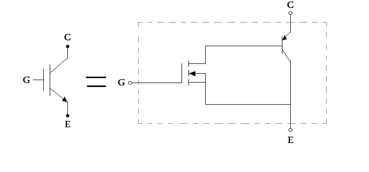
IGBT (Insulated - gate bipolar transistor)This is an insulated gate bipolar transistor (IGBT) - a three-electrode power electronic device, used mainly as a powerful electronic switch in switching power supplies, inverters, and in electric drive control systems. The IGBT graphic symbol is shown in the figure below. In its internal structure, the IGBT is a cascade connection of two electronic keys: the input key on the field-effect transistor controls a powerful terminal key on the bipolar transistor. The control electrode is called a gate, like a field-effect transistor, the other two electrodes are called an emitter and a collector, like a bipolar one. Such a composite inclusion of field and bipolar transistors allows you to combine the advantages of both types of semiconductor devices in one device. Currently, power IGBT modules are available for currents from 10 to 2400 A and switching voltage up to 3.3 kV. Often you can find intelligent power modules (IPM - Intelligent power module). Intelligent Power Modules (IPM) modules are distinguished by the presence of a control board that contains sensors, protection driver circuits, and diagnostics.
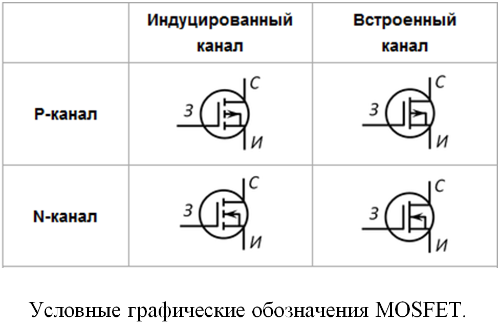
MOSFET (metal-oxide-semiconductor field effect transistor) is a MOS structure (metal - oxide - semiconductor) - the most widely used type of field effect transistor. The structure consists of a metal and a semiconductor, separated by a layer of silicon dioxide (SiO2). In the general case, the structure is called MIS (metal - dielectric - semiconductor). Transistors based on MOS structures are called field effect, or MOS transistors. Graphic symbols are shown in the figure.
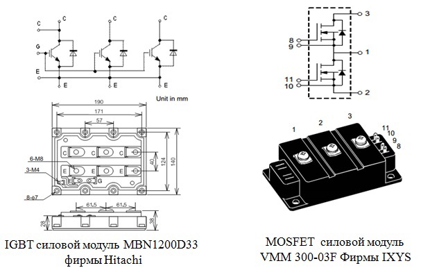
An example of IGBT and MOSFET power modules is shown in the figure below.
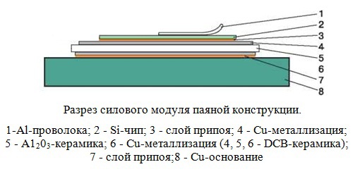
These power modules are created using DCB technology (Direct Copper Bonding), which literally translates as direct landing on copper. The figure shows a section of a DCB power module.
Lead-free solder is used as solder in modern power devices, which imposes a number of limitations on the characteristics of the devices. The low melting point of lead-free solder (≈ 250 ° C) imposes restrictions on the maximum working temperature of 100 - 120 ° C, which makes it impossible to assemble a DCB structure using a gallium arsenide chip or silicon carbide, whose operating temperature is above 200 ° C . Also, solder does not withstand thermal cycling - heating to maximum temperature and subsequent cooling. After several thousand cycles, pores appear cracked on the solder.
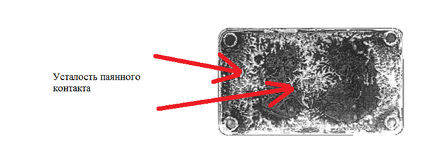
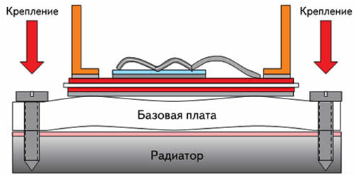
Due to different coefficients of thermal expansion (KTP of silicon = 4 μm / mK, KTP of solder = 25-30 μm / mK), different parts of the transistor expand differently, which leads to a bending of the structure. Due to bending, contact with the radiator worsens, and in the worst case scenario the silicon chip may crack. This phenomenon is called the bimetallic effect. Due to the bimetallic effect, it is not possible to assemble structures with a silicon chip whose diameter exceeds 100 mm. You can solve this problem if you use material with a lower CTE as solder than lead-free solder. Such a material is a paste sinter (KTP = 19-20 μm / mK).
Sinter paste
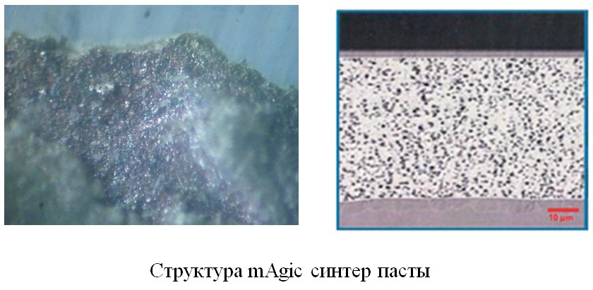
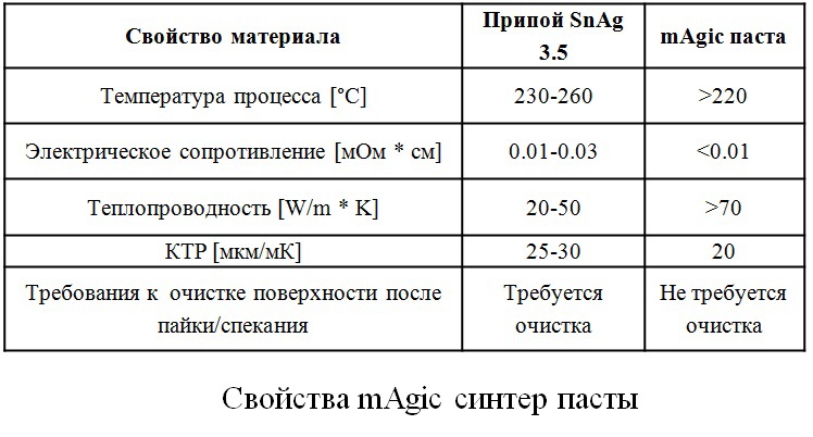
Sinter paste is a silver powder with solvents. Since the technology of sinter pastes is quite new, there is no established term in Russian that could be called them. Literal translation sounds like sinter pasta. After sintering, the sinter paste is pure silver, all solvents evaporate. The structure is shown below. The grain size is from 0.1 to 1 micron. On the left is a photograph of a real sample, on the right is a drawing from the documentation for the sinter paste mAgic sinter paste from Herause. The table below compares sinter paste and lead-free solder. It can be seen that sinter paste has better thermal and electrical conductivity, as well as a lower KTP value.
Sinter paste is sintered in 2 stages. Before sintering, sinter paste is applied to the connected surfaces by screen printing. The thickness of the layer is 150 microns. The first stage is pre-drying at a temperature of 80 ° C for 15 minutes. Then it is sintered at a pressure of 30 MPa and a temperature of 270 ° C for 5 minutes. Sintering without pressure is allowed for chips with a diameter of more than 150 mm.

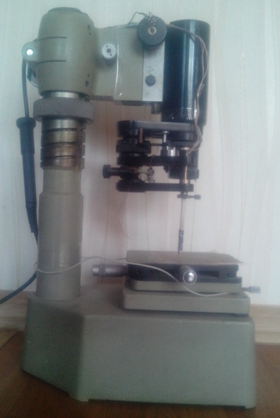
To study the properties of sinter paste, DCB structure models were used. As DCB ceramics, 2 mm thick copper plates were used. When applying, a stencil with a thickness of 150 μm was used, in which a 10 by 10 mm square hole was made. To study the homogeneity of sinter paste, the thermo-EMF method was used. For this, a thermo-EMF measurement installation was assembled. As a heater, a heater from a soldering iron of a Lukey 702 soldering station was used. The temperature setter was the same soldering station. A tungsten needle was attached to the heater. The values of thermo-EMF were measured with a UT71D multimeter. All this was mounted on a bed from a PMT-3 microscope, which has a micrometer table and a spring-loaded suspension on which the heater is mounted.
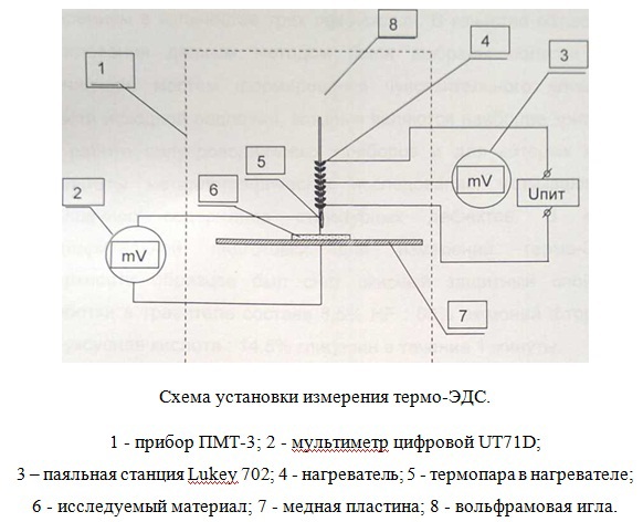
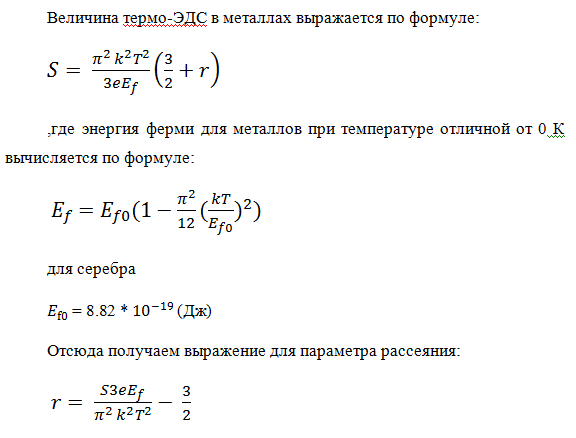
Samples sintered at various pressures (10, 20, 30, 40, and 50 MPa) were measured on this setup. Measurements were taken in increments of 1 mm. Heater temperature 320 ° C. After the measurements, a matrix of 10 by 10 values was obtained. The scattering parameter r was chosen as a criterion for uniformity. It is derived from the value of thermo-EMF as follows:
The results are tabulated, and the dependence of uniformity on sintering pressure is constructed.
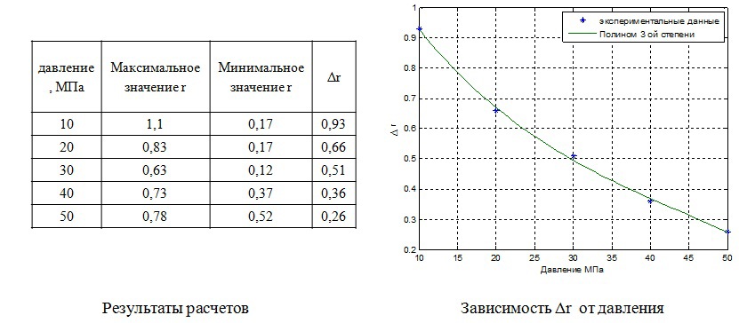
From the results it can be concluded that uniformity increases with increasing pressure, but with increasing pressure it becomes more difficult to observe the plane-parallelism of the connected parts, which can lead to damage to the silicon chip.
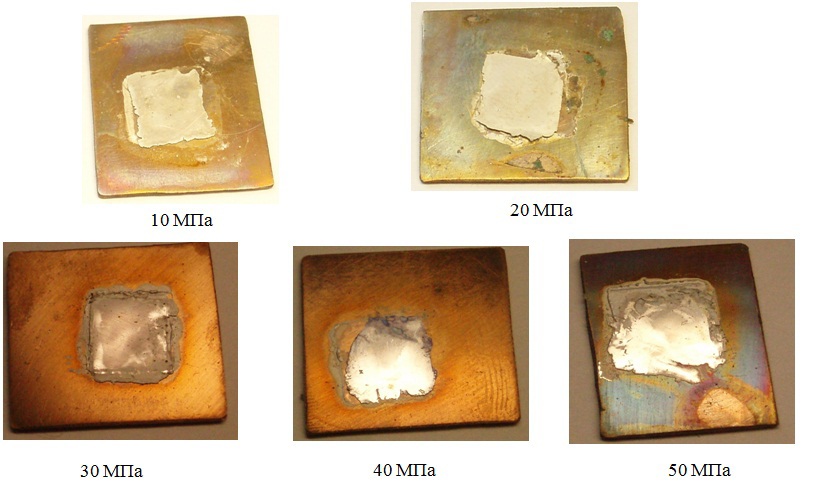
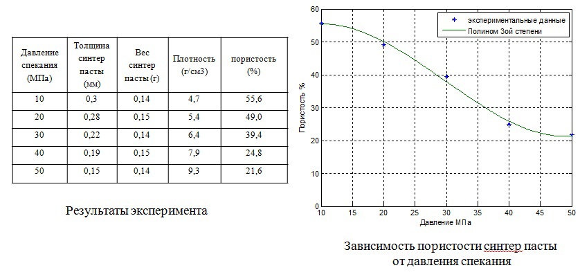
To study the dependence of the porosity of the sinter paste on pressure, 5 samples were sintered at pressures of 10 to 50 MPa. On specimens sintered at a pressure of 30 MPa and higher, specular gloss regions are visible, which indicates that in these regions the density approaches the density of silver. Since, after sintering, the contact is pure silver, then by calculating the contact density and comparing it with the silver density one can find out the porosity of the sinter paste. The contacts were separated from the copper base, measured with a micrometer and weighed on electronic scales. The measurement results and calculations are summarized in the table, according to which a graph of the dependence of porosity on the sintering pressure is constructed.
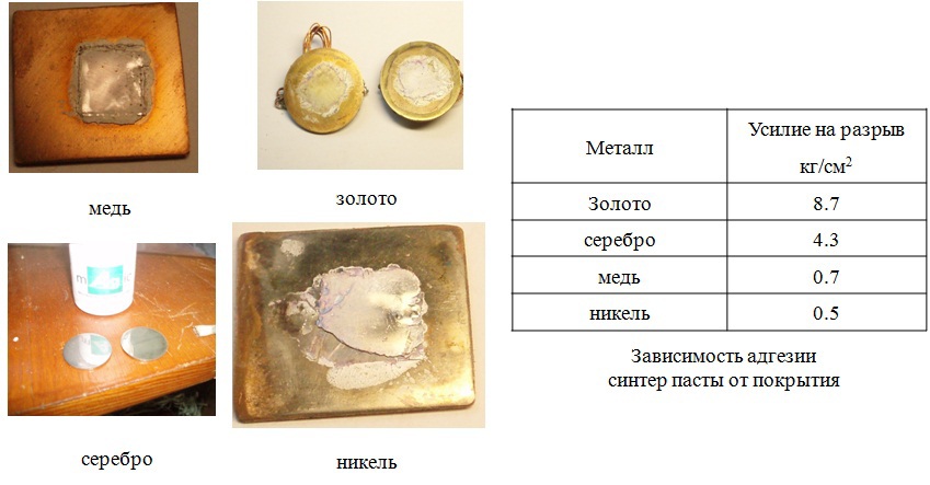
To study the dependence of the adhesion of the sinter paste on the coating, 4 samples were prepared, sintered at a pressure of 30 MPa. Gold, silver and nickel coatings were used. The last sample was uncoated. As can be seen from the table, gold proved to be the best, copper the worst.
Conclusion
Sinter paste is suitable for use in power semiconductor modules as a replacement for lead-free solder. The best indicators of heat and electrical conductivity can increase the power of devices while maintaining the same dimensions. A higher melting point allows the use of silicon carbide and gallium arsenide chips that can operate at temperatures of 200 ° C and higher. Also, sinter paste does not degrade its properties as a result of thermal cycling, which increases the reliability of the devices.