Have you seen your printed circuit boards under a microscope?
I make printed circuit boards myself, LUTom.
The first stage is the transfer of the picture. After - check the quality of the transfer of toner to the board. If all is well, we’ll hurt. Somewhere the track fell off, the landfill adhered poorly - it doesn’t matter, a felt-tip pen in hand and forward. Etched? We inspect the board for the integrity of the tracks / heels / polygons / different symbols, etc.
Looking at my brainchild once again, it dawned on me: “What if you look at the board through a microscope?” Of course, I’ll notice a broken wire, but it’s interesting to look at the smallest details: the edges of the tracks, the middle of the holes. (Caution - a lot of photos!)
So, let's get started.
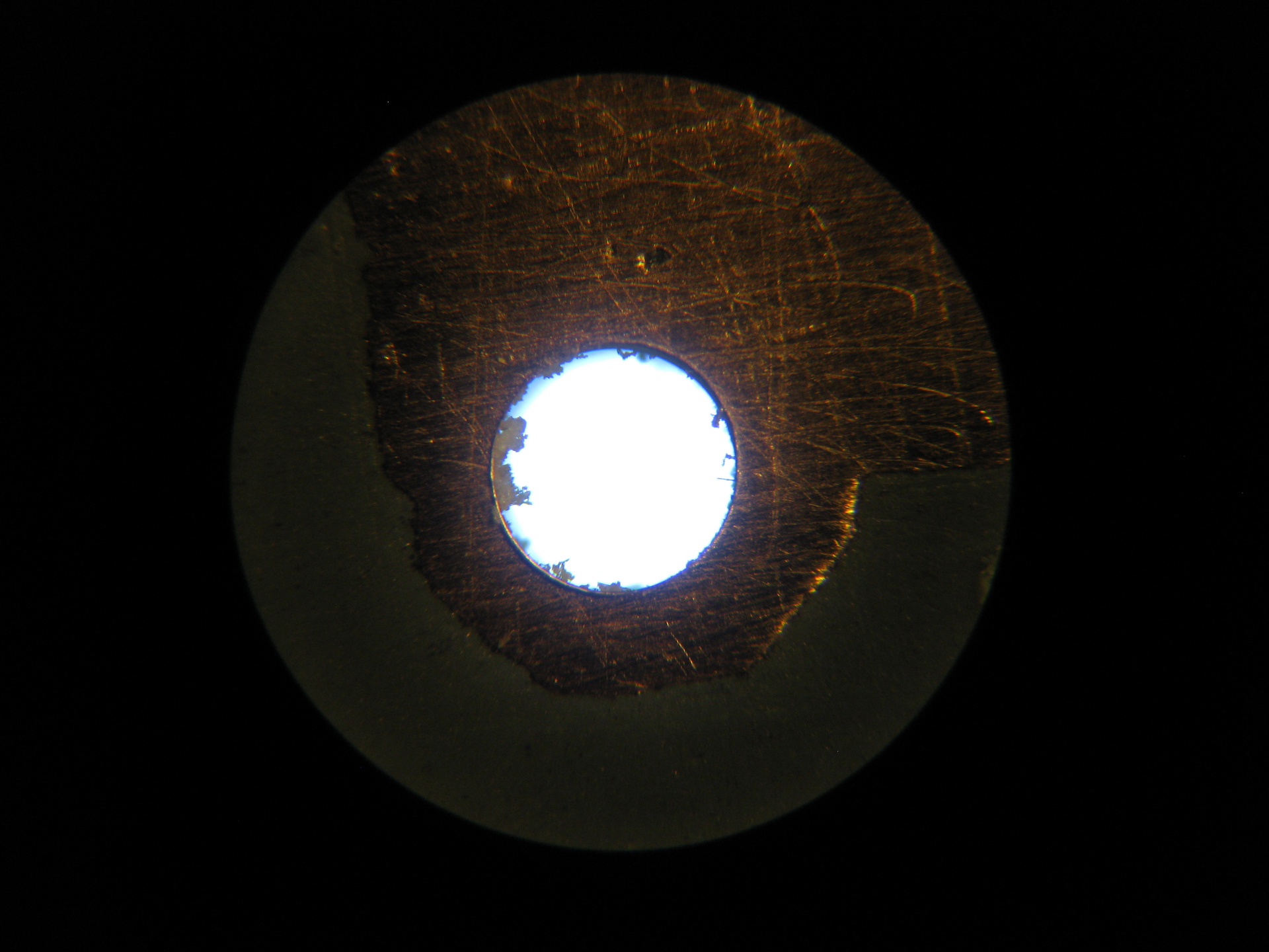
1. The entire board, just etched, on the microscope stage:

The holes for the components have not yet been drilled.
2. The area for the smd component:

It can be seen that the toner has already started to depart. Fortunately, this did not happen during etching.
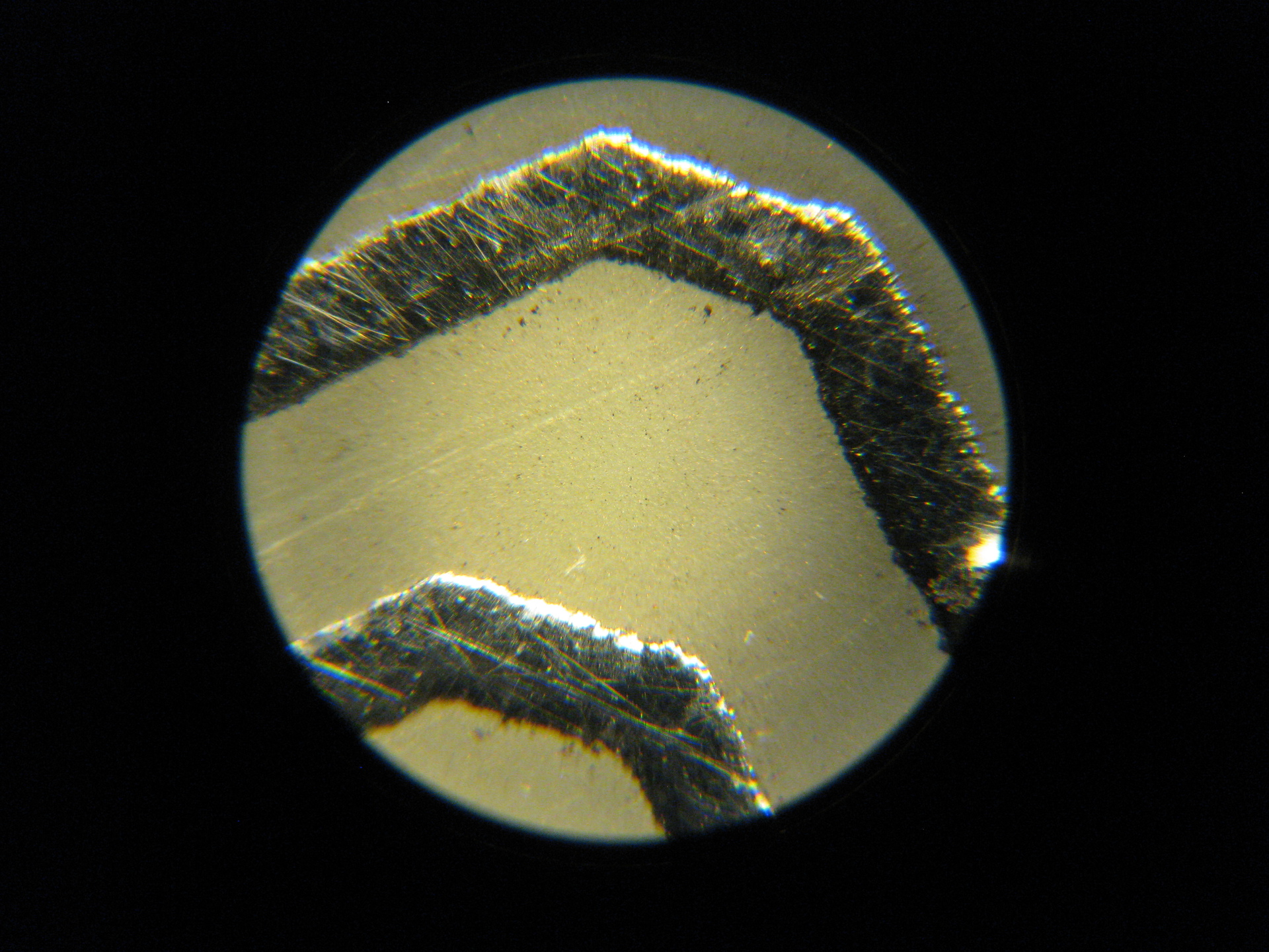
3. Another site, but already for the output part:

Toner, also, is not all present.
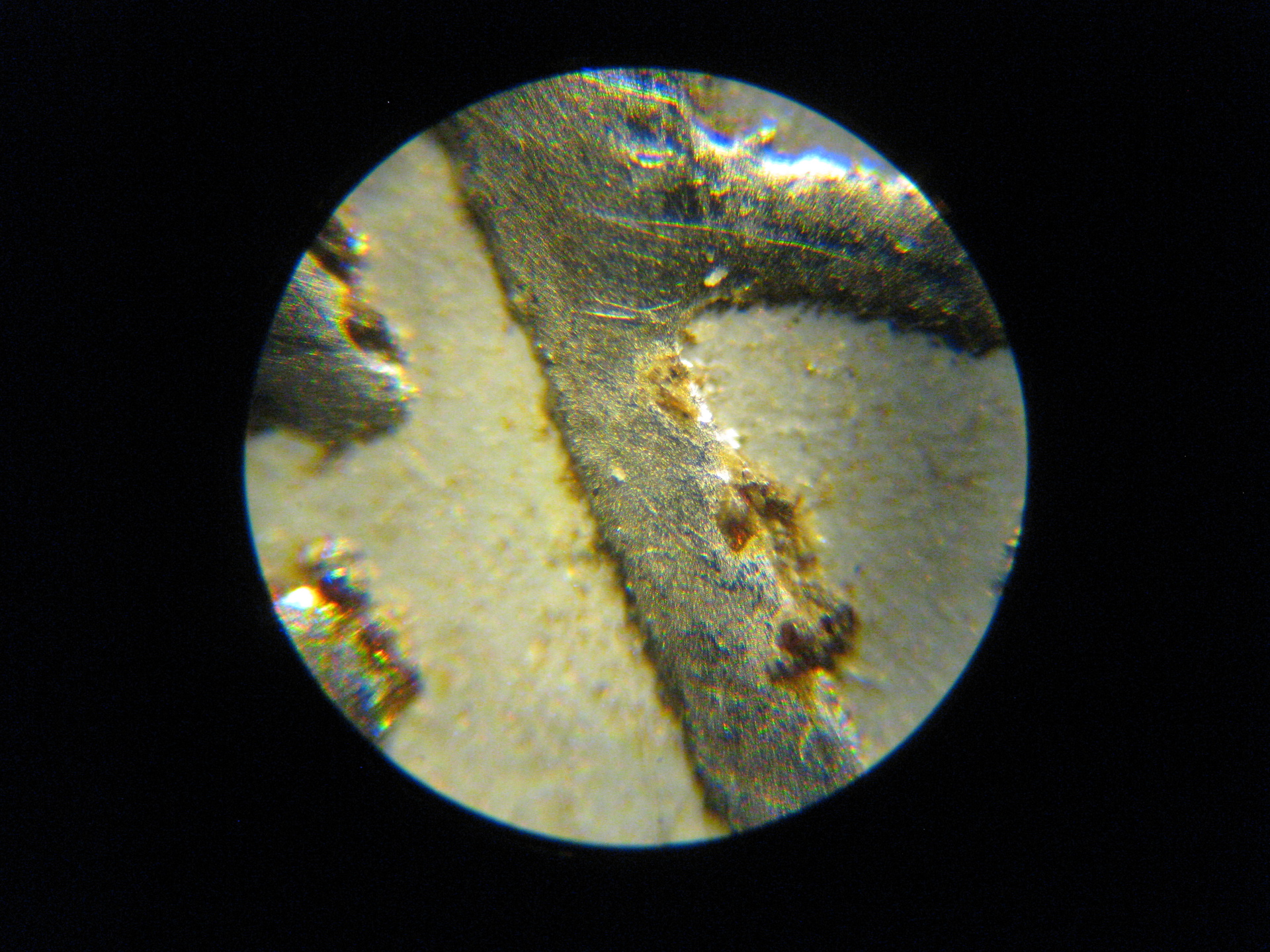
4. And the microcircuit will get here. The toner has peeled off, but an almost perfect path is visible under it:

5. Oval area. Apparently, the toner on the board did not fit very well on it, as a result of which, the necessary copper partially “left”.

6. Tracks. With a width of 0.4, it turned out pretty well.

7. Remember, I said that in the right places the board can be tinted with a marker?


8. This track FeCl 3 did not spare:

9. The edges of the polygons do not always turn out to be smooth:

10. Here, too much was etched:

11. Have you noticed a small figure eight near the place for the chip?

12. Pad for the output part:

13. Unidentified object on the board: The

photo did not work out very well, because it’s very small.
14. Drilled holes, sanded:


15. Striped tracks:

16. Pad with a hole. You can see how the drill broke the back of the board:
17. The letters on the board. Notice how many chips are around:

18. That's it! The fee is tinned (the tracks are the same, from No. 6):
19. The unwashed flux between the tracks and letters:

It is not for nothing that, apparently, they advise to wash it off.
20. Tinned eight:

21. More tinned components:


As you can see, even not very even and damaged parts are well tinned and now look neat.
22. And finally. Board edge:

Now you understand why they are advised to clean / level?
For sim - that's it. Thanks for attention.
Z.Y. These are far from the most worthy representatives of LUT technology. Using a laser iron, one can make tracks 0.1 mm wide. What attracts LUT to me is:
Of course, this technology also has its drawbacks. I will not write about them anymore, I think everyone knows them for himself.
Another photo:


LUT on magazine paper. The board is made the first time. It took ~ 5 minutes to transfer the pattern and strip the board (the time for heating the iron is also taken into account). Tracks 0.254 mm, distance 0.4096 mm. Of course, there are drawbacks, but such boards will work. When speed of production is important - IMHO, the most suitable way.
The first stage is the transfer of the picture. After - check the quality of the transfer of toner to the board. If all is well, we’ll hurt. Somewhere the track fell off, the landfill adhered poorly - it doesn’t matter, a felt-tip pen in hand and forward. Etched? We inspect the board for the integrity of the tracks / heels / polygons / different symbols, etc.
Looking at my brainchild once again, it dawned on me: “What if you look at the board through a microscope?” Of course, I’ll notice a broken wire, but it’s interesting to look at the smallest details: the edges of the tracks, the middle of the holes. (Caution - a lot of photos!)
So, let's get started.
1. The entire board, just etched, on the microscope stage:
The holes for the components have not yet been drilled.
2. The area for the smd component:
It can be seen that the toner has already started to depart. Fortunately, this did not happen during etching.
3. Another site, but already for the output part:
Toner, also, is not all present.
4. And the microcircuit will get here. The toner has peeled off, but an almost perfect path is visible under it:
5. Oval area. Apparently, the toner on the board did not fit very well on it, as a result of which, the necessary copper partially “left”.
6. Tracks. With a width of 0.4, it turned out pretty well.
7. Remember, I said that in the right places the board can be tinted with a marker?
8. This track FeCl 3 did not spare:
9. The edges of the polygons do not always turn out to be smooth:
10. Here, too much was etched:
11. Have you noticed a small figure eight near the place for the chip?
12. Pad for the output part:
13. Unidentified object on the board: The
photo did not work out very well, because it’s very small.
14. Drilled holes, sanded:
15. Striped tracks:
16. Pad with a hole. You can see how the drill broke the back of the board:
17. The letters on the board. Notice how many chips are around:
18. That's it! The fee is tinned (the tracks are the same, from No. 6):
19. The unwashed flux between the tracks and letters:
It is not for nothing that, apparently, they advise to wash it off.
20. Tinned eight:
21. More tinned components:
As you can see, even not very even and damaged parts are well tinned and now look neat.
22. And finally. Board edge:
Now you understand why they are advised to clean / level?
For sim - that's it. Thanks for attention.
Z.Y. These are far from the most worthy representatives of LUT technology. Using a laser iron, one can make tracks 0.1 mm wide. What attracts LUT to me is:
- board manufacturing speed;
- cost compared to photoresist (materials are cheaper);
- the ability to work less with chemistry.
Of course, this technology also has its drawbacks. I will not write about them anymore, I think everyone knows them for himself.
Another photo:
LUT on magazine paper. The board is made the first time. It took ~ 5 minutes to transfer the pattern and strip the board (the time for heating the iron is also taken into account). Tracks 0.254 mm, distance 0.4096 mm. Of course, there are drawbacks, but such boards will work. When speed of production is important - IMHO, the most suitable way.
Only registered users can participate in the survey. Please come in.
And using what technology do you make printed circuit boards?
- 68.3% LUT 689
- 17.5% Photoresist 177
- 20.9% Chinese 211
- 10.3% Other 104