How did we do Wiren Board
Over the past 9 months we have been developing Wiren Board - a compact industrial computer with many built-in interfaces (Wi-Fi, GPRS, GPS, NFC, Ethernet, etc.) We already wrote about it, and received a bunch of reviews and suggestions. As a result, a lot of changes were made to the new version, and this article is about the most significant of them.
Compared with the April prototype, 2 USB-host, RS-485 interface and a connector with 8 GPIO appeared on the board. In addition, we made a new power circuit that supports input voltages from 5 to 22 volts, Passive PoE and Li-Pol battery connections, added low-voltage load control and analog inputs on the terminal blocks.
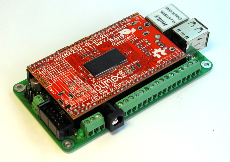
How we did this, what difficulties we encountered and what happened in the end, read our article.
Wiren Board with processor module removed:

Inside, usually covered by the processor module:

In the new version of Wiren Board, we added the ability to connect analog signals and sensors (digital, resistive, dry contact sensors), as well as low-voltage load control.
The SoC we use has two 12-bit common ADC channels. To increase the number of available ADC channels, we use the SN74HC4851 multiplexer, which connects one of the 8 channels to the input of the ADC processor.

One ADC channel is used to measure the supply voltage, seven are output through the resistors to the terminal blocks. To protect the outputs from high voltages, resistors are enough, since the multiplexer has built-in protective diodes. The ADC channel of our SoC has a programmable current source. The values of the resistors were selected so that when the current source is turned on, it is possible to measure the resistance of the resistive sensors.
To control the low-voltage load (motors, LED strips, locks, etc.), it is convenient to use “open collector” outputs (see Fig.).
To save space, the analog inputs were combined with low-voltage load control channels. The disadvantage of this solution is the small current flowing through the closed output at voltages above 3.3 V.
The task was to come up with a power scheme for the board. The requirements for the power scheme are as follows:
Other conditions:
Solution:
Since it is supposed to power the circuit from the battery, it is impossible to do without a boost DC-DC converter for a 5V line. An inexpensive NCP1450 chip was chosen (as it turned out later, not the best choice). This is a step-up DC-DC converter with an external transistor.
The voltage on the Li-Pol battery is 2.7..4.2V, but the “plateau” on the discharge curve is in the region of 3.7V. Therefore, to get 3.3V, it is quite possible to use LDO.
We chose the linear regulator MCP1826, it provides current up to 1A. Given the requirements of the GSM modem for voltage and current, it should be connected directly to the battery. And it's better to add more capacitors. So, while a circuit is developing in which everything is connected to the battery.
And then it’s not so obvious.
To charge the battery requires a special microcircuit, which will properly charge it. It is impossible to charge with ordinary DC-DC, because it is necessary to maintain a constant voltage (4.2V) with high accuracy and limit the charging current (CC / CV mode). But for the possibility of working without a battery, you can not do without a step-down DC-DC converter!
To resolve this contradiction, power management systems are used.
In our case, it would look something like this:

But this option did not suit us in terms of cost and footprint.
We decided to make a feint with our ears and went the other way.

LTC4002 is a simple and inexpensive Li-Ion battery charger with a PWM controller that works as a step-down DC-DC converter. The charger operates in constant current / constant voltage mode: it maintains a constant charging current until the battery voltage reaches 4.2V. After that, it maintains a constant voltage of 4.2 V on the battery with great accuracy.
The microcircuit determines the charging current by measuring the voltage drop across the external R_sense resistor using the SENSE input. After that, the charging current is set to I_c = 100mV / Rsense.
For small batteries of 1500-2000 mAh, the charging current should not exceed 500-700 mA, and the power circuit should provide up to 2 A in pulse mode for the GSM module. To fulfill these two conditions at the same time, you have to “trick” the LTC4002.
Using two Rsense resistors, we achieve that the charging current of the battery is no more than 100mV / (R1 + R2), and the current to the load is up to 100mV / R1.
We check: we poison the scarf with the power circuit, assemble, everything works fine. The voltage gives out as it should, the battery is charging.
We order a board in Rezonit, collect the entire circuit, turn it on - it does not work.
We look at the oscilloscope - it turns out that the NCP1450 (5V boost converter) produces the right voltage, but not current :) Without a load, the output is 5 volts, as expected. But a small load of 10 mA - and the voltage drops to the input.
A ceramic capacitor is required in the power line as close to the NCP1450 legs as it was advised in the datasheet :) 1 cm from the legs - and it doesn’t work anymore. You also need the output capacitor to be at least 330 μF. Capricious chip, in the next version we will change.
Okay, soldered more capacitors - it works.
We put on Olinuxinka (our processor board is OLinuXino-MICRO), turn it on - it does not work. Turn it off, turn it back on - it works.
It turns on randomly with a probability of ~ 50%. Magic.
Reason: The
LTC4002 charger has a tricky mode of charging half-dead batteries, in which it tries to charge the battery with a current of 10% of the nominal (trickle charging mode).
The mode turns on when the voltage on the battery is less than 2.9V, and the boost converter by 5V starts to work from 2.2V.
And here is who is faster: if the LTC4002 manages to charge the output capacitors to 2.9V faster than the converter starts to work, then the power will turn on and continue to work normally. If it doesn’t have time, then the NCP1450 starts consuming current, the voltage does not reach 2.9V, and the LTC4002 considers our system a dead battery without increasing the current.

We will have to assemble a circuit that will disconnect the load until the voltage rises to 3V in order to “slip through” the trickle-charging mode of the LTC4002.
Well, we put a bipolar transistor with an ultra-low voltage drop and a three-output zener diode (aka programmable voltage reference, aka shunt regulator) to its base.
Resistor R3 sets the base current, the divider R4-R5 sets the threshold voltage for switching on, and positive feedback through R6 creates a small hysteresis on-off - 3.1-2.9V. Resistor R7 provides the minimum cathode current.
At the same time, this solution will protect the battery from overdischarge and allow you to make the power button. With one crutch, we solve three problems!
We continue testing the board with the power circuit.
Input voltage 5V - everything works! 12 volts - the NFC stops working, cannot read the card: ((
Reason:
the power circuit creates strong interference that interferes with the NFC.
Can it be the unshielded coils?
Ok, turn the coils to the side so that their field lines become perpendicular to the NFC antenna. We
check. 12 volts - works, 22V (we supply power via PoE) - does not work. So you have to install shielded coils, although they are twice as large.
Okay, we ’ll add filter capacitors to the right places in the power circuit.
And now NFC works in the entire input range stresses.
We check the operation under load on the 3.3V and 5V lines of 0.5 A. Using an IR thermometer, we control the temperature of the elements, the board heats up a little, but everything is within reasonable limits.
But at 22V, the Schottky diode burns out in ten seconds.
Diode PMEG3010 - at 30V 1A. In the step down converter circuit, the higher the voltage, the greater the current flows through the diode at the same output power.
Ok, put a diode more powerful.
We redraw the board for shielded coils, add filtering capacitors, and shorten the tracks with pulsed currents as much as possible. We change the burned Schottky diode to a 2 ampere one, transfer it to the outside and draw polygons for it for better cooling.
We test the board - the diode burns out in the same 10 seconds: ((It's time to carefully read the datasheets for these diodes.
Carefully looking at the graphs, we notice that the reverse current through the Schottky diode exponentially depends on both the temperature and the applied voltage. And at a voltage of 22V, a 30V diode does not have such a small reverse current. The breakdown mechanism is approximately the following: while the diode is cold, the reverse current is very small, and the diode is heated only by direct current. The diode warmed up a bit - the reverse current increases and increases the heating. The temperature rises - the current is even greater.
And now - an avalanche-like rise in temperature and the end.
In practice, it looks like this - turn on, the diode is cold, warm, even warmer, burned out.
In general, you need to read the datasheets very carefully and not believe what they write on the first page.
At this point, I want to convey fiery greetings to the NXPmarketing engineers who actually write these datasheets. Here's an example of a Schottky diode PMEG4050. Declared specifications: 40V reverse voltage, 5A maximum current. Looks good!
However, if you read what exactly is written in small print, it turns out that 5A is measured at an air temperature of 0 degrees (sic!) For a diode soldered to a ceramic printed circuit board. So the question is, why was it not to write honest 3 amperes in the characteristics? The riddle.
As a result, we put a diode with a voltage of 40V, the circuit works stably and without overheating. We got a workable power scheme, which is used in the first series of devices.
Despite the fact that in the end we got an inexpensive and stable power supply scheme throughout the range, we already had a couple of ideas on how to improve it. Firstly, you can replace the linear stabilizer for the 3.3V line with a compact step-down DC-DC converter. In addition, you can change the boost converter for the 5V line to a less demanding and higher frequency chip. Such a conversion will slightly increase the efficiency and free up space on the board for another module.
A detailed description of the Wiren Board and the wiki with documentation is here .
The first small batch of 55 Wiren Board we have assembled in Russia and distribute them among developers and users. Looking forward to your feedback!
UPD: devices from the first batch still remain, you can buy them on our website
- Wiren Board Team
Compared with the April prototype, 2 USB-host, RS-485 interface and a connector with 8 GPIO appeared on the board. In addition, we made a new power circuit that supports input voltages from 5 to 22 volts, Passive PoE and Li-Pol battery connections, added low-voltage load control and analog inputs on the terminal blocks.
How we did this, what difficulties we encountered and what happened in the end, read our article.
What and where on the board?
Wiren Board with processor module removed:
Inside, usually covered by the processor module:
Analog inputs and outputs
In the new version of Wiren Board, we added the ability to connect analog signals and sensors (digital, resistive, dry contact sensors), as well as low-voltage load control.
The SoC we use has two 12-bit common ADC channels. To increase the number of available ADC channels, we use the SN74HC4851 multiplexer, which connects one of the 8 channels to the input of the ADC processor.
One ADC channel is used to measure the supply voltage, seven are output through the resistors to the terminal blocks. To protect the outputs from high voltages, resistors are enough, since the multiplexer has built-in protective diodes. The ADC channel of our SoC has a programmable current source. The values of the resistors were selected so that when the current source is turned on, it is possible to measure the resistance of the resistive sensors.
To control the low-voltage load (motors, LED strips, locks, etc.), it is convenient to use “open collector” outputs (see Fig.).
To save space, the analog inputs were combined with low-voltage load control channels. The disadvantage of this solution is the small current flowing through the closed output at voltages above 3.3 V.
Power Adventures
The task was to come up with a power scheme for the board. The requirements for the power scheme are as follows:
- The output current on the 3.3V and 5V buses is at least 500mA for connecting USB, UEXT modules, and more.
- To power the GSM modem, you need to provide voltage from 3.5V to 4.6V, with pulse currents up to 2A and voltage drops of no more than 300mV.
- Ability to work from a Li-Ion battery, charging the battery. Battery overcharge protection.
- Extended input voltage range, at least 5-15V.
Other conditions:
- Do not use chips in cases without legs - QFN, DFN and the like - mounting them in Russia is very expensive
- Low cost
- Minimum dimensions
Solution:
Since it is supposed to power the circuit from the battery, it is impossible to do without a boost DC-DC converter for a 5V line. An inexpensive NCP1450 chip was chosen (as it turned out later, not the best choice). This is a step-up DC-DC converter with an external transistor.
The voltage on the Li-Pol battery is 2.7..4.2V, but the “plateau” on the discharge curve is in the region of 3.7V. Therefore, to get 3.3V, it is quite possible to use LDO.
We chose the linear regulator MCP1826, it provides current up to 1A. Given the requirements of the GSM modem for voltage and current, it should be connected directly to the battery. And it's better to add more capacitors. So, while a circuit is developing in which everything is connected to the battery.
And then it’s not so obvious.
To charge the battery requires a special microcircuit, which will properly charge it. It is impossible to charge with ordinary DC-DC, because it is necessary to maintain a constant voltage (4.2V) with high accuracy and limit the charging current (CC / CV mode). But for the possibility of working without a battery, you can not do without a step-down DC-DC converter!
To resolve this contradiction, power management systems are used.
In our case, it would look something like this:
But this option did not suit us in terms of cost and footprint.
We decided to make a feint with our ears and went the other way.
LTC4002 is a simple and inexpensive Li-Ion battery charger with a PWM controller that works as a step-down DC-DC converter. The charger operates in constant current / constant voltage mode: it maintains a constant charging current until the battery voltage reaches 4.2V. After that, it maintains a constant voltage of 4.2 V on the battery with great accuracy.
The microcircuit determines the charging current by measuring the voltage drop across the external R_sense resistor using the SENSE input. After that, the charging current is set to I_c = 100mV / Rsense.
For small batteries of 1500-2000 mAh, the charging current should not exceed 500-700 mA, and the power circuit should provide up to 2 A in pulse mode for the GSM module. To fulfill these two conditions at the same time, you have to “trick” the LTC4002.
Using two Rsense resistors, we achieve that the charging current of the battery is no more than 100mV / (R1 + R2), and the current to the load is up to 100mV / R1.
We check: we poison the scarf with the power circuit, assemble, everything works fine. The voltage gives out as it should, the battery is charging.
Miracles 1
We order a board in Rezonit, collect the entire circuit, turn it on - it does not work.
We look at the oscilloscope - it turns out that the NCP1450 (5V boost converter) produces the right voltage, but not current :) Without a load, the output is 5 volts, as expected. But a small load of 10 mA - and the voltage drops to the input.
A ceramic capacitor is required in the power line as close to the NCP1450 legs as it was advised in the datasheet :) 1 cm from the legs - and it doesn’t work anymore. You also need the output capacitor to be at least 330 μF. Capricious chip, in the next version we will change.
Okay, soldered more capacitors - it works.
Miracles 2
We put on Olinuxinka (our processor board is OLinuXino-MICRO), turn it on - it does not work. Turn it off, turn it back on - it works.
It turns on randomly with a probability of ~ 50%. Magic.
Reason: The
LTC4002 charger has a tricky mode of charging half-dead batteries, in which it tries to charge the battery with a current of 10% of the nominal (trickle charging mode).
The mode turns on when the voltage on the battery is less than 2.9V, and the boost converter by 5V starts to work from 2.2V.
And here is who is faster: if the LTC4002 manages to charge the output capacitors to 2.9V faster than the converter starts to work, then the power will turn on and continue to work normally. If it doesn’t have time, then the NCP1450 starts consuming current, the voltage does not reach 2.9V, and the LTC4002 considers our system a dead battery without increasing the current.
Bring to mind
We will have to assemble a circuit that will disconnect the load until the voltage rises to 3V in order to “slip through” the trickle-charging mode of the LTC4002.
Well, we put a bipolar transistor with an ultra-low voltage drop and a three-output zener diode (aka programmable voltage reference, aka shunt regulator) to its base.
Resistor R3 sets the base current, the divider R4-R5 sets the threshold voltage for switching on, and positive feedback through R6 creates a small hysteresis on-off - 3.1-2.9V. Resistor R7 provides the minimum cathode current.
At the same time, this solution will protect the battery from overdischarge and allow you to make the power button. With one crutch, we solve three problems!
Miracles 3
We continue testing the board with the power circuit.
Input voltage 5V - everything works! 12 volts - the NFC stops working, cannot read the card: ((
Reason:
the power circuit creates strong interference that interferes with the NFC.
Can it be the unshielded coils?
Ok, turn the coils to the side so that their field lines become perpendicular to the NFC antenna. We
check. 12 volts - works, 22V (we supply power via PoE) - does not work. So you have to install shielded coils, although they are twice as large.
Okay, we ’ll add filter capacitors to the right places in the power circuit.
And now NFC works in the entire input range stresses.
Miracles 4
We check the operation under load on the 3.3V and 5V lines of 0.5 A. Using an IR thermometer, we control the temperature of the elements, the board heats up a little, but everything is within reasonable limits.
But at 22V, the Schottky diode burns out in ten seconds.
Diode PMEG3010 - at 30V 1A. In the step down converter circuit, the higher the voltage, the greater the current flows through the diode at the same output power.
Ok, put a diode more powerful.
About the benefits of reading datasheets
We redraw the board for shielded coils, add filtering capacitors, and shorten the tracks with pulsed currents as much as possible. We change the burned Schottky diode to a 2 ampere one, transfer it to the outside and draw polygons for it for better cooling.
We test the board - the diode burns out in the same 10 seconds: ((It's time to carefully read the datasheets for these diodes.
Carefully looking at the graphs, we notice that the reverse current through the Schottky diode exponentially depends on both the temperature and the applied voltage. And at a voltage of 22V, a 30V diode does not have such a small reverse current. The breakdown mechanism is approximately the following: while the diode is cold, the reverse current is very small, and the diode is heated only by direct current. The diode warmed up a bit - the reverse current increases and increases the heating. The temperature rises - the current is even greater.
And now - an avalanche-like rise in temperature and the end.
In practice, it looks like this - turn on, the diode is cold, warm, even warmer, burned out.
In general, you need to read the datasheets very carefully and not believe what they write on the first page.
Lyrical digression
At this point, I want to convey fiery greetings to the NXP
However, if you read what exactly is written in small print, it turns out that 5A is measured at an air temperature of 0 degrees (sic!) For a diode soldered to a ceramic printed circuit board. So the question is, why was it not to write honest 3 amperes in the characteristics? The riddle.
As a result, we put a diode with a voltage of 40V, the circuit works stably and without overheating. We got a workable power scheme, which is used in the first series of devices.
Plans
Despite the fact that in the end we got an inexpensive and stable power supply scheme throughout the range, we already had a couple of ideas on how to improve it. Firstly, you can replace the linear stabilizer for the 3.3V line with a compact step-down DC-DC converter. In addition, you can change the boost converter for the 5V line to a less demanding and higher frequency chip. Such a conversion will slightly increase the efficiency and free up space on the board for another module.
Conclusion
A detailed description of the Wiren Board and the wiki with documentation is here .
The first small batch of 55 Wiren Board we have assembled in Russia and distribute them among developers and users. Looking forward to your feedback!
UPD: devices from the first batch still remain, you can buy them on our website
- Wiren Board Team