Layfkhaki manufacturing double-layer boards (LUT)
The need to make iron periodically occurs in many techies. Sometimes the task allows nafigachit all the wires on the breadboard, and sometimes, unfortunately, you need something more serious. One day, the need to make printed circuit boards overtook me ... Laser-iron technology for making handicrafts at first strongly repels its randomness (what to print, how to warm, how much to press, how to tear, etc.), but friends shared their experience and it turned out that it is really not that difficult. LUT is unquestionably cheaper than any other option, and (suddenly) is quite suitable for dual layer boards.
Anyone interested is more complicated, more expensive and more accurate, you can make a photoresist , but our technique (the main element of which is a special paper) allows us to stably work tires of 0.3 / 0.3 mm, so that in our community there is an opinion thattyan photoresists are not needed.
Whoever does not see the point in the handicraft production of boards, most likely will be able to recall a couple of cases when they had to cut the tracks and solder the wiring for the whole batch of boards. And by making one board at home, you can properly debug it and gain confidence in the factory boards.
Under the cut, I will share the deterministic method of manufacturing two-layer printed circuit boards using LUT technology with different backup circuits in case of jambs. From idea to inclusion. We will work with KiCad, Inkscape, sandpaper, iron, ammonium persulphate and engraver.
Any device starts with a circuit. Most board errors can be fixed at the design stage. And to ensure that the scheme is consistent with the board, you need a good EDA-software. For example, KiCad.
KiCad -> Fee
If you are still working with proprietary limited solutions, start with the article Tracing PCBs in KiCAD or skip this section.
We use the recently released KiCad 5, because I deeply like this program, its community (including CERN) and the idea of multiplatform FOSS as a whole.
So, the algorithm with life hacks :
- Find a component in the catalog of your favorite electronics store.
- Find the corresponding component in the KiCad library.
- If it is a transistor or another component with three or more pins, find its case in the Pcbnew footprint library, look at the numbering, compare it with the datasheet and select the component with the correct numbering of the pins in Eeschema.

- If the component is not in the KiCad library, look for it on the Internet. If it still doesn’t exist, we find a similar one in the library, export Symbol (to a new library), connect it to the project, open it in the Symbol library editor, refine it, do the same with footprint if the case is also non-standard.
- If there is a completely equivalent choice, we give preference to components that have a 3D model. KiCad can show how the device will look, it greatly helps to find errors.
- If it is a transistor or another component with three or more pins, find its case in the Pcbnew footprint library, look at the numbering, compare it with the datasheet and select the component with the correct numbering of the pins in Eeschema.
- We place the component on the scheme, in the Datasheet field of the component we place a link to this component from the store .
- We draw the scheme without forgetting:
- Use tires and tags to avoid overloading the circuit with a bunch of parallel lines.
- Giving names to chains not included in tires and tags to make it easier to navigate on the board.
- Persist.
- Put the project under git and commit.
- Associate components with footprints, number components, generate a netlist, generate Bill of Materials (which will contain a list of links and the number of elements next to each link, so that you can go straight to the basket and order the elements right away.
- Open Pcbnew, download the netlist.
- Configure DRC:
- For signal circuits, the minimum width of the tracks is 0.3 mm, clearance 0.3 mm.
- For more power, proportional to the strength of the current. There are online calculators.
- Default Via - 0.8 with holes 0.6.
- Of course, if there is a place on the board, all these dimensions (except the holes) should be made the maximum possible, because if Via is 1 mm, then the probability of getting into it with a drill from another layer is extremely high))
- Well, Via 0.8 is not a hard minimum size at all: if a thick path fits the hole, then you can at least put 0.5, there is still something convenient to be soldered to.
- Manually draw a board, following the advice from article 7 of the design rules for printed circuit boards .
- I, too, at first seemed to be "FE, the car should do it," but then once I tried it and my world would no longer be the same. Manual tracing is much more interesting and fun than it seems. I advise everyone, especially those who like to collect puzzles.
- In addition, the machine will not follow the 7 rules for designing printed circuit boards , and it may take longer to fix autotrace than to do manual tracing.
- If you are not convinced, or you have a VERY difficult board, well, take an ax ...
- Add labels and logos.
- To put the KiCad logo on one of the copper layers, you need to export the footprint, open it in a text editor and change "F.SilkS" to "F.Cu" in all polygons.
- Add 4 0.35 / 0.5 overall holes in the board corners at a distance of ~ 5-10 mm from the Edge.Cuts layer lines
Fee -> SVG
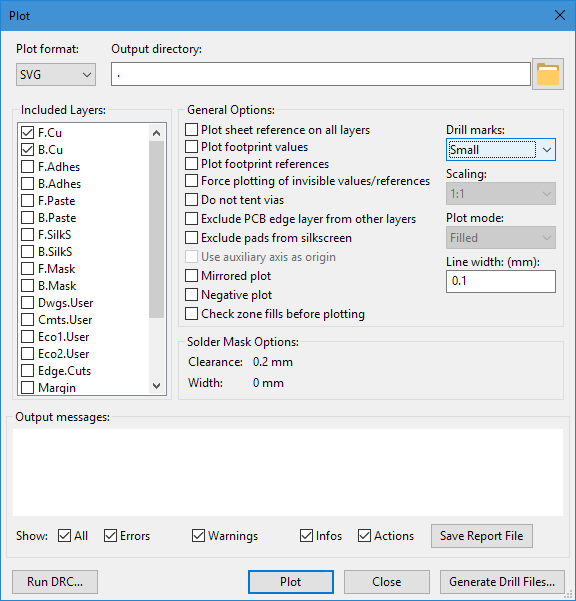
When the board is ready, you need to overtake it in SVG for further refinement. It is better to unload the board from EDA without mirroring, so as not to get confused and mirror it properly.
A mirror your need only front layer F.Cu . Since we look at the back layer of B.Cu in the editor from the front, it is already mirrored. For reliability, it is better to place at least some text on both layers and make sure that this text is not read))
( thank you , dShaded ) From KiCad it is better to upload via File | Plot , since there it is possible to make all the holes 0.35 mm at once. For LUT, fat holes are not needed, it is better to have more copper and it will be cleaned with a drill.
Actually:
- Load both layers into Inkscape.
- Set the unit of measurement of the document millimeters, and the format of an A4 sheet .
- Add more white lettering on the areas of metallization . KiCad does not know how, write in the comments if your EDA can.
- We group together so that there are only two objects.
- Smooth (Ctrl + Shift + A), the distance between the layers (their overall holes) must be at least a centimeter.
- Mirror the front layer with a button on the upper toolbar.
- Save to SVG.
Now you need to send SVG to the printer on plain paper. And do the following with this paper:
- Add components to it and check footprints (which have already come from the store anyway: if you have more than three or five components on the board, it’s difficult to trace everything in one evening)
- Attach to the PCB and thread 4 dimensional holes in the corners that we added
- Take a core (or nail) with a hammer and make an ultra-precise shallow dent absorbing lost drills. The impact force must be such as not to deform the board.
- Drill 4 holes with the thinnest drill bit (0.6-0.8) at exactly 90 degrees. This is perhaps the most difficult part, but errors are conditionally permissible; The way of their subsequent correction is invented.
- If there is a machine, you are lucky.
- If there is a CNC, you are lucky enough, figure all the holes in the DRL file right now without any cores- * ernov.
- It is easy to guess that the holes are necessary for precise orientation of the front layer relative to the back. If you want it easier, there is a way without holes: very precisely fold a piece of paper with a template and place the textolite inside. As already mentioned, a slight deviation will not be fatal (unless, of course, the holes have not been drilled yet)
- Another modification of the folding shared TonnyRed :
Freshly printed sheets with the top and bottom layers put on each other, shining through the lamp and combining. We fasten in several places along the edges. In the resulting envelope put textolite.- Another (much more advanced) way of orienting layers is shared by dgrees . Thank!
Tax, this is a section about SVG, and we have already moved to the machines ... That's all, the last touch on SVG and more computers will not be needed:
Fill everything around with black so that the PCB parts that do not belong to the board are not etched and do not saturate the ammonium persulfate with copper. Yes, ferric chloride is also possible, but ammonium is blue.
SVG -> Textolite
The whole article is, in fact, written only in order to share with the world the most correct paper for LUT. Here she is:
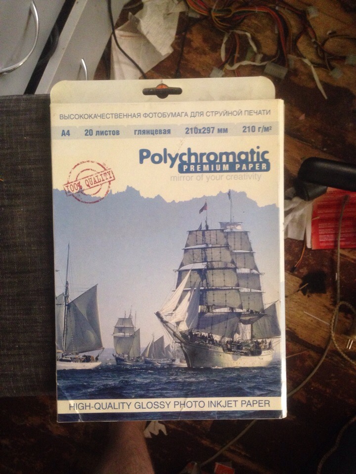
Also, we have information on the benefits of Black Diamond paper . Other brands may have the necessary properties, but may not. HP does not fit exactly (melts under the iron), Lomond conditionally fits, "but somehow medium . " You can experiment with different glossy inkjet photo paper . Write in komenty cho as with other papers)
oco advises using a roasting sleeve. It is a transparent film, does not melt under the iron and is easily removed from the board, leaving the toner. The printer is refilled with a sheet of plain paper.
Algorithm:
- We put the iron to bask at the maximum temperature.
- We grind the PCB on both sides with fine sandpaper, sanitary abrasive sponge ( thanks , klirichek ), dishcloth sponge or abrasive eraser.
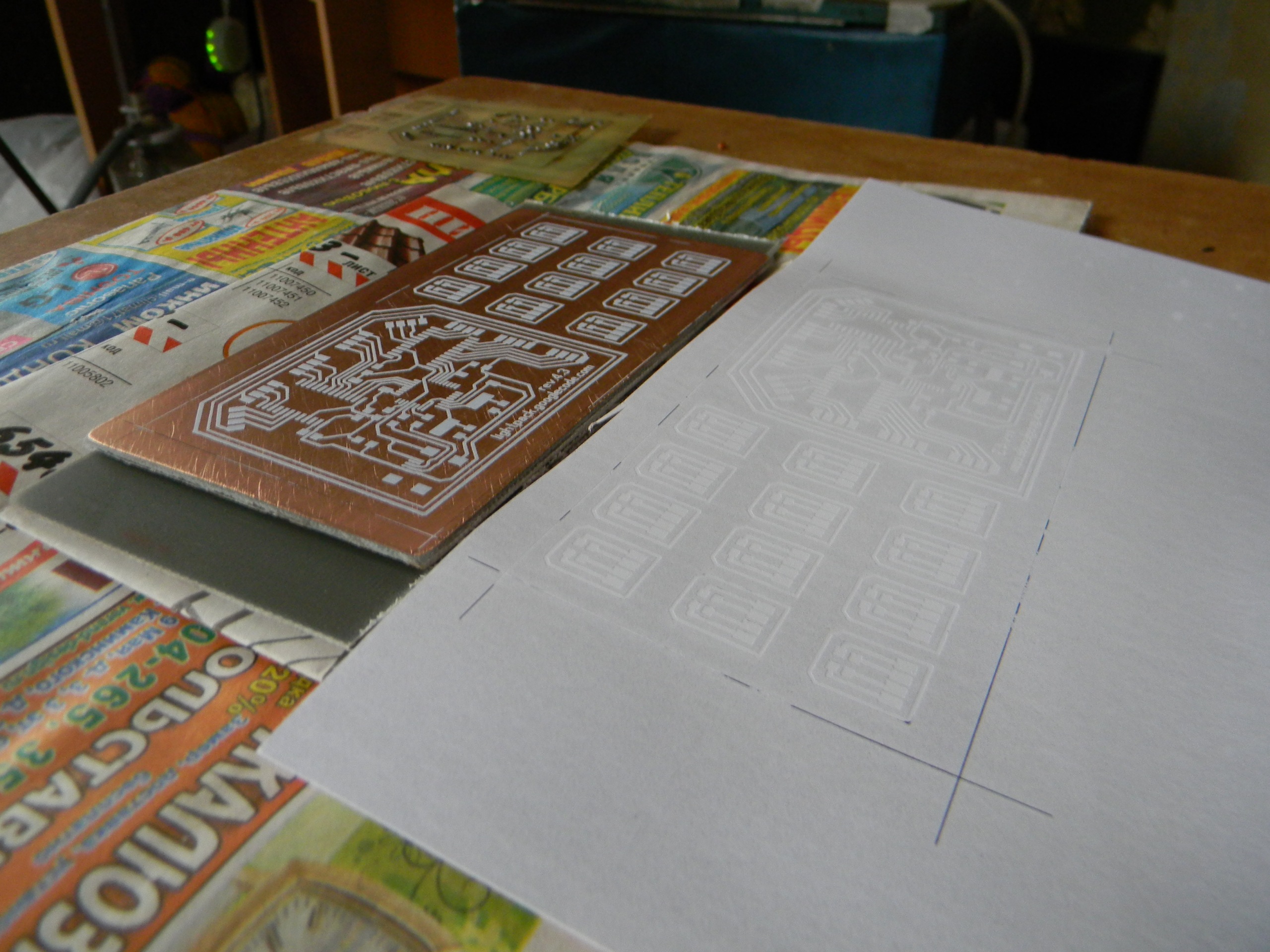
- If your printer knows how to eat formats other than A4, we cut off the strip from A4 to fit the image. Paper overvalued: if you managed to get it, you need to save.
- We push in the printer narrow side. We check that the image of the two layers of the board does not exceed the width of the cut strip in width and 210 in height.
- We print lazer with original toner in the cartridge on this glossy photo paper for inkjet printers.
- Without touching the toner, we cut the layers into two separate pieces of paper and perforate the overall holes on both layers.
- Insert straight pins (for example, from a PLS / PLD comb) into 4 dimensional holes.
- We put the front layer.
- We iron it evenly, without pressing hard, until the paper turns yellow (or any other signs above, it’s still LUT: it’s probably impossible to completely get rid of magic). The pins can be pulled out when the paper sticks and loses its ability to move.
- Without tearing the paper from the PCB, repeat the last three points with the back layer.
- Let the textolite cool: for now, you can put a kettle on and warm up the ammonium persulfate.
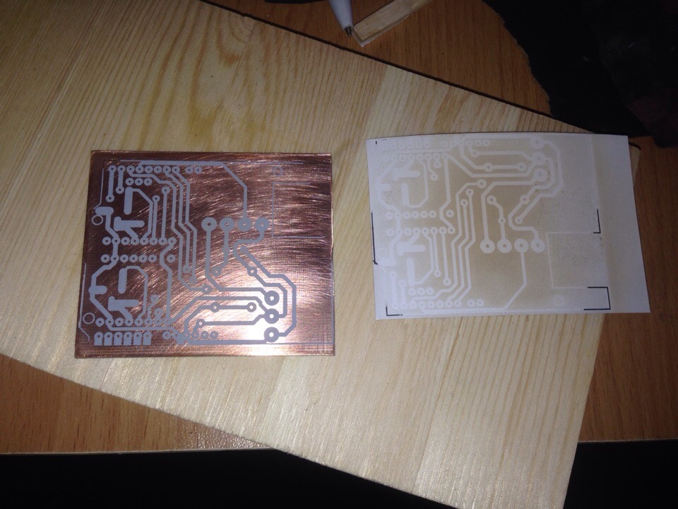
- From the cooled PCB (without water, it is extremely important) to carefully tear off the excess paper . Toner should go along with a glossy layer of photo paper, and it was intended.
In case of errors, you can erase one of the layers with acetone, put the already torn piece of paper of the opposite layer (so that the toner does not detach from the board and does not transfer to the board on which you iron) and repeat.
Textolite -> Textolite with tracks
For pickling, we will need a plastic container (or any non-metal container in which the board will fit while lying). And also, a disposable spoon or varibis for stirring the board (against bubbles that interfere with etching).
Ammonium persulphate is recommended to be diluted in warm water 1: 2. But this is a fairly high concentration, 1: 3 or even 1: 4 is enough. In the end, you can still mix up the sweat. Recommended temperature reassurance - 40-50 degrees.
However, please note that overheating all kinds of chemicals is quite dangerous. High concentration, high temperature and copper salts can lead to a creep effect:
https://vk.com/video-24764675_456239191
Use a respirator.
It is advisable to move the board, blow bubbles from it and maintain the temperature in the region of 35-45 degrees in a water bath. But if the persulfate is not dead, it can itself be maintained (see video above).
If poorly poisoned, you can:
- Buy new ammonium, it loses its properties when stored in conditions of high humidity
- Stop stirring
- Still wait
- Pull out the board and reheat the solution in the microwave (neat)
- Shred some more white powder
Thank you, Helium4 for advice in a personal on this section.
After etching, the toner is wiped off with acetone.
Textolite with tracks -> Fee
It remains to drill and connect vias.
Layfkhak: If it so happened that there is a displacement of layers, it can be compensated for by the angle of inclination of the drill .
From the first hole it is difficult to catch the desired angle, so it is better to first drill the least demanding holes to the exit point (for example, those that go to the metallization area or bulk copper islands)
After drilling, it is necessary to connect the holes. Of course, we will do this with the help of resistor / capacitor legs and a soldering iron. But sometimes it is necessary to put an SMD component on top of the transition hole, and in this case, a high solder bun is unacceptable. We came up with the following trick:
- Seal pin
- We grind down all unnecessary engraver
- ....
- Profit!
You can also order and use rivets , thanks to tretyakovmax for reminding them (True, his way of ripping up a patchcord lived - this seems to be a topic for a separate article)
If you still made a mistake and etched a layer with components that have more than two mirrored conclusions, try to bend the legs of the components in the opposite direction and solder them upside down.
Like all))
You can solder components and cut in power.
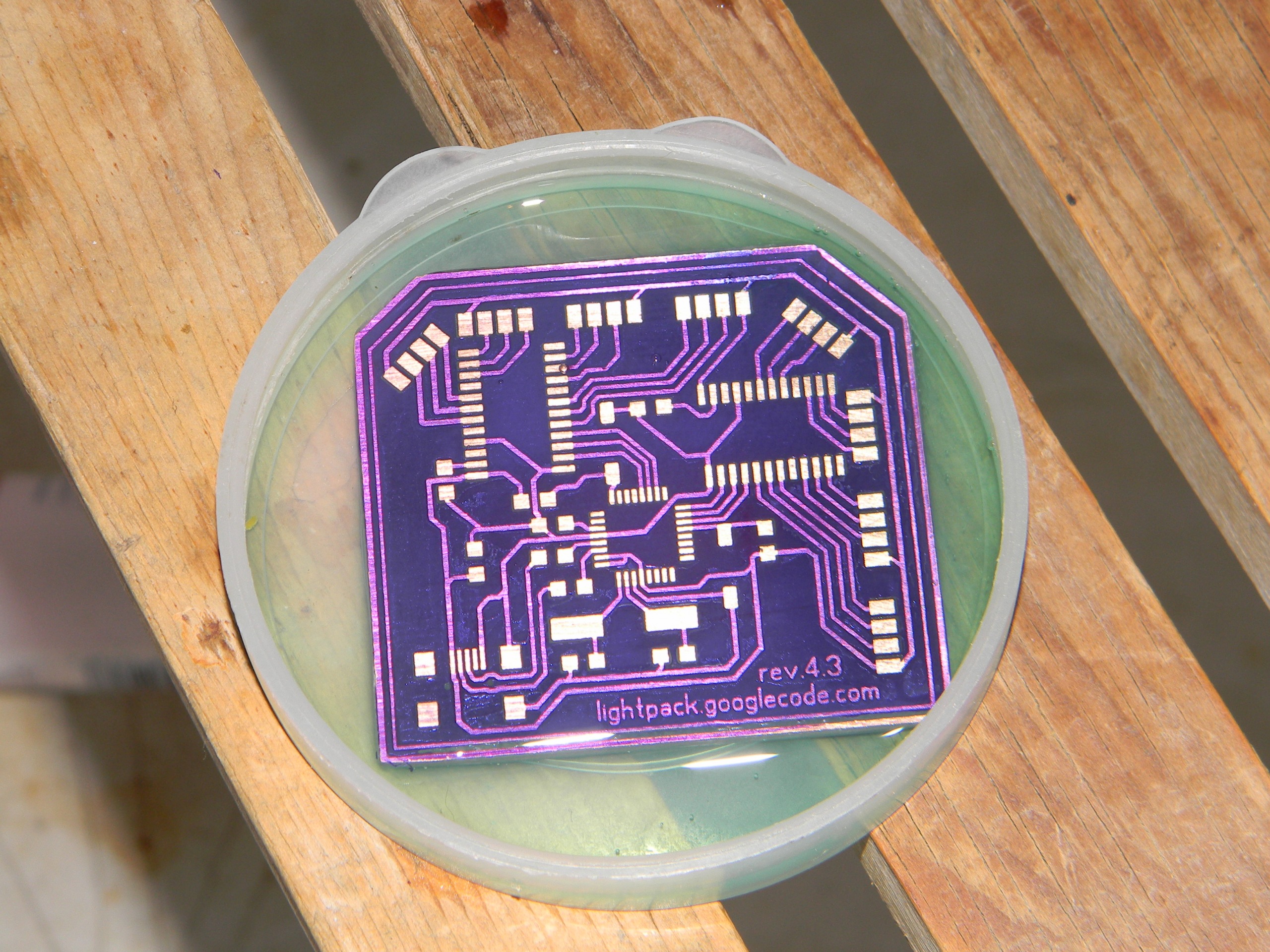
After testing and correcting, fix vias, transfer text and logos to the silk-screen layer and order purple boards on OSHPark , or many boards on EasyEDA .
The board at KDPV is indeed manufactured by LUT, and not ordered from OSHPark. Purple solder mask solves :)
Here is another suitable vidos for the further study of all kinds of subtleties (carefully, sticky channel, there are victims):
Thanks for attention!