Hardware interrupt handling in intel architecture. i8080 - i80486, PIC, ISA, conventional PCI
The topic gives an overview in historical perspective of the mechanisms used to interface external devices with an x86 architecture CPU.
The i8080 has a set of eight single-byte RSTn commands: RST0 - RST7, functionally equivalent to calling CALL routines at fixed addresses n * 8.
The i8080 interrupt processing unit is connected to two dedicated legs:
In the first cycle of each machine cycle, the i8080 sends a status word to the data bus, the zero bit of which (INTA, interrupt acknowledge) signals the confirmation of the interrupt.
The only difference between the interrupt cycle and the usual cycle of fetching the instruction code from memory is that the processor does not increase the address of the instruction counter; after receiving the interrupt request, the processor as usual reads the command code from the data bus (in cycle T3 of cycle M1, see fig.). The task of the interrupt controller is to understand by the status word that the interrupt request has been accepted and put a suitable command on the data bus. The command can be arbitrary, usually RSTn or CALL.

The interrupt processing cycle is described in detail on page 2-11 [0].
The i8086 has 256 INTn instructions in the instruction set: INT 0 - INT 0ffh, and a table of 256 addresses. Each INTn instruction prohibits interrupts, saves the flag register and command counter on the stack, and jumps to the address recorded in the nth element of the interrupt table.
The i8086 interrupt processing unit is connected to three dedicated legs:
In addition, the output signals of the processor S0 # - S2 # indicate in a manner similar to the i8080 the type of the current machine cycle. The combination 000 corresponds to the interrupt acknowledgment cycle.
The interrupt processing cycle is described in detail on page 11 [1].
Despite the fact that the software side of interrupt handling has changed significantly with the advent of protected mode, page addressing and 32-bit instructions, the hardware side of delivering interrupt requests to the processor has undergone minimal changes.
The highlighted interrupt confirmation signal INTA # has disappeared. The number of machine cycle status signals increased to 4 in i80286, then decreased to 3; the combination 0000/000 still indicates an interrupt acknowledgment cycle. The interrupt reception still generates two confirmation cycles, the interrupt vector is read from bits D0-D7 of the data bus at the end of the second cycle. Starting with i80386, the address bus bit A2 is set to 1 on the first and 0 on the second interrupt acknowledgment cycle.
Typical Picture (i80386):
Details on page 3-33[2] , in clause 5.4.4 [3] and clause 7.2.10 [4] .
With the release of the i8085 processor, Intel released a programmable interrupt controller (PIC) - i8259 [5] . This controller, capable of working with both the i8080 and x86, was used almost unchanged in models from IBM PC to IBM PC / AT based on i80486. With the advent of SMP chipsets, it began to be slowly superseded by the combination of IO-APIC (I / O advanced PIC) i82093 + LAPIC (local APIC) i82489.
The controller has the following characteristics:
Simplified logic of the controller is as follows:
Early domestic developments based on the i8080 (KR580VM80), such as Micro-80 and Radio-86RK, did not use the interrupt mechanism. Later ones, for example, UT-88, used periodic interrupts for the timer, sending a low-frequency signal to INT input and not controlling the data bus in the confirmation cycle (on the free bus, all data bits were read as 1, forming the RST7 command).
In the west, the Altair 8800 S-100 bus has become the de facto standard later adopted as IEEE-696 [6] . The bus provided an INT * interrupt request signal intended for the master and 8 dedicated lines of vectorized interrupts. It was understood that a certain interrupt controller would convert the vectorized interrupt signals into an INT * request and form a vector in the confirmation loop.
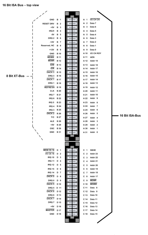
ISA (industry standard architecture) was developed by IBM in 1981 for an IBM PC and in the PC and PC / XT models had an eight-bit data bus and 5 IRQ3 - IRQ7 interrupt request lines connected to the corresponding inputs of a single interrupt controller. IRQ0 connected to the timer, and IRQ1 to the keyboard controller. Starting with PC / AT, a second interrupt controller appeared in cascade connected to the IRQ2 of the first i8259, the data bus expanded to 16 bits, the ISA connector lengthened and IRQ10-12, 14 and 15 lines appeared in it.
Traditionally (at least for MS-DOS ) interrupt controllers are initialized to work on the front of the IRQ with the base vectors 8 and 0x70, so that IRQ0 calls INT 8, IRQ1 - INT 9, IRQ8 - INT 70h, IRQ9 - INT 71h, etc.
Chipsets for ISA, eg i82340SX [7], contain in their composition an unchanged cascade of two 8259A and essentially do not differ from the original PC / AT design in this regard.
PCI (peripheral component component interconnect) was developed by Intel in 1993. One of the goals Intel pursued when developing this bus was to design independence from the processor / motherboard architecture. For interrupts, the consequences of this solution are as follows:
Chipsets for PCI, for example PIIX [8], have dedicated legs for INTA # ... INTD # inputs connected to interrupt request lines coming from PCI connectors. To combine the functionality of the required ISA and PCI, the chipsets began to add registers, allowing you to choose for each interrupt, it is activated by level or front, as well as reassign IRQ number corresponding to some IRQ # inputs within certain limits. But basically the interrupt controller in these chipsets is still a cascade of two 8259.
[0] Specification i8080: arcarc.xmission.com/Tech/CPU/8080/8080.pdf
[1]I8086 specification: datasheets.chipdb.org/Intel/x86/808x/datashts/8086/231455-005.pdf
[2]Specification i80286: datasheets.chipdb.org/Intel/x86/286/datashts/intel-80286.pdf
[3]Specification i80386: datasheets.chipdb.org/Intel/x86/386/datashts/23163011.pdf
[4]Specification i80486: datasheets.chipdb.org/Intel/x86/486/datashts/240440-006.pdf
[5]Specification i8259A: pdos.csail.mit.edu/6.828/2005/readings/hardware/8259A.pdf
[6]IEEE696 specification: https://web.archive.org/web/20120330015830/http://www.imsai.net/download/IEEE_696_1983.pdf
[7]82340SX Chipset Specification (ISA): www.datasheetarchive.com/pdf/download.php?id=7307256284271468fbe93b200907c75d7727e3&type=O&term=823400X
[8]Chipset Specification 82371 (PIIX) pdf.datasheetcatalog.com/datasheet/Intel/mXvqwzr.pdf
Spoiler
I realized that I would never finish this grandiose review in its entirety, so I just removed “Part 1” from the name. Perhaps this part will still be useful to someone.
Processor interface
i8080 [0]
The i8080 has a set of eight single-byte RSTn commands: RST0 - RST7, functionally equivalent to calling CALL routines at fixed addresses n * 8.
The i8080 interrupt processing unit is connected to two dedicated legs:
- INTE (interrupt enabled) - an output reflecting the readiness of the processor to accept the interrupt. The EI and DI commands, enable and disable interrupts, set respectively high and low level on this pin. A low level is set on this pin also after receiving an interrupt request.
- INT - interrupt request input. A high level signal at this input, provided there is a high level at the INTE output, initiates an interrupt processing cycle at the end of the current command.
In the first cycle of each machine cycle, the i8080 sends a status word to the data bus, the zero bit of which (INTA, interrupt acknowledge) signals the confirmation of the interrupt.
The only difference between the interrupt cycle and the usual cycle of fetching the instruction code from memory is that the processor does not increase the address of the instruction counter; after receiving the interrupt request, the processor as usual reads the command code from the data bus (in cycle T3 of cycle M1, see fig.). The task of the interrupt controller is to understand by the status word that the interrupt request has been accepted and put a suitable command on the data bus. The command can be arbitrary, usually RSTn or CALL.
The interrupt processing cycle is described in detail on page 2-11 [0].
i8086 [1]
The i8086 has 256 INTn instructions in the instruction set: INT 0 - INT 0ffh, and a table of 256 addresses. Each INTn instruction prohibits interrupts, saves the flag register and command counter on the stack, and jumps to the address recorded in the nth element of the interrupt table.
The i8086 interrupt processing unit is connected to three dedicated legs:
- NMI (non-maskable interrupt) - non-maskable interrupt input, the rising edge of the signal at this input leads to the execution of the INT 2 instruction at the end of the current command;
- INTR (interrupt request) - input of the interrupt request. A high level signal at this input, provided the processor is ready to accept the interrupt, initiates the interrupt processing cycle at the end of the current command.
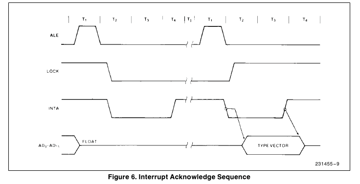
- INTA # (interrupt acknowledge) - interrupt acknowledgment output. When an interrupt is received, the i8086 generates two confirmation cycles, during which the INTA # signal is switched to the active (low) state. On the rising edge of this signal in the second cycle, the processor reads from the data bus 8 bits D0-D7, called the interrupt vector, and executes the command INTn, where n is the value of the read byte. The task of the interrupt controller is to place the interrupt vector on the data bus at this moment.
In addition, the output signals of the processor S0 # - S2 # indicate in a manner similar to the i8080 the type of the current machine cycle. The combination 000 corresponds to the interrupt acknowledgment cycle.
The interrupt processing cycle is described in detail on page 11 [1].
i80286 - i80486 [2] [3] [4]
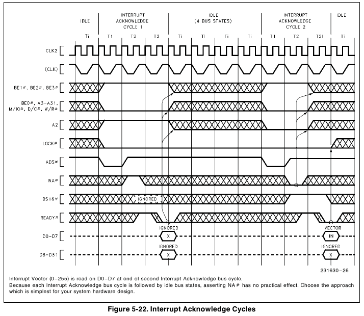
Despite the fact that the software side of interrupt handling has changed significantly with the advent of protected mode, page addressing and 32-bit instructions, the hardware side of delivering interrupt requests to the processor has undergone minimal changes.
The highlighted interrupt confirmation signal INTA # has disappeared. The number of machine cycle status signals increased to 4 in i80286, then decreased to 3; the combination 0000/000 still indicates an interrupt acknowledgment cycle. The interrupt reception still generates two confirmation cycles, the interrupt vector is read from bits D0-D7 of the data bus at the end of the second cycle. Starting with i80386, the address bus bit A2 is set to 1 on the first and 0 on the second interrupt acknowledgment cycle.
Typical Picture (i80386):
Details on page 3-33[2] , in clause 5.4.4 [3] and clause 7.2.10 [4] .
Interrupt controller
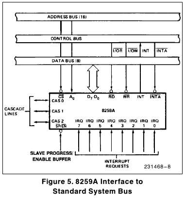
With the release of the i8085 processor, Intel released a programmable interrupt controller (PIC) - i8259 [5] . This controller, capable of working with both the i8080 and x86, was used almost unchanged in models from IBM PC to IBM PC / AT based on i80486. With the advent of SMP chipsets, it began to be slowly superseded by the combination of IO-APIC (I / O advanced PIC) i82093 + LAPIC (local APIC) i82489.
The controller has the following characteristics:
- 8 inputs IRQ (interrupt request) interrupt request from external devices;
- receiving an interrupt request by level or edge of the IRQ signal (general setting for all IRQ inputs);
- each IRQ input can be masked independently of the others;
- Several IRQ prioritization modes the ability to dynamically change IRQ priorities;
- the possibility of combining into a two-level cascade as a master or slave (64 independent IRQ lines in the maximum configuration);
- programmable base interrupt vector;
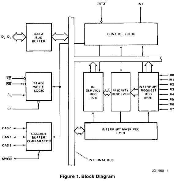
Simplified logic of the controller is as follows:
- signals on IRQ lines are recorded in the internal IRR register. If the controller is level, the IRR bits are reset when the IRQ signal level drops;
- as soon as bits are set in the IRR that are not masked by the current mask (in the IMR register), the controller issues an INT signal to the processor or master controller;
- upon the arrival of the first confirmation of the interrupt (signal INTA #), the controller finds the unmasked IRR bit with the highest priority, sets it in the ISR register (interrupts in processing) and clears it in the IRR. If no suitable bits are found in the IRR, bit 7 is set;
- upon the arrival of the second signal, the INTA # controller generates an interrupt vector with a value on the data bus (basic interrupt vector + IRQ number in processing);
- at the command to complete the interrupt processing (from the processor or automatic), the corresponding bit of the ISR register is cleared;
Tires
Early domestic developments based on the i8080 (KR580VM80), such as Micro-80 and Radio-86RK, did not use the interrupt mechanism. Later ones, for example, UT-88, used periodic interrupts for the timer, sending a low-frequency signal to INT input and not controlling the data bus in the confirmation cycle (on the free bus, all data bits were read as 1, forming the RST7 command).
In the west, the Altair 8800 S-100 bus has become the de facto standard later adopted as IEEE-696 [6] . The bus provided an INT * interrupt request signal intended for the master and 8 dedicated lines of vectorized interrupts. It was understood that a certain interrupt controller would convert the vectorized interrupt signals into an INT * request and form a vector in the confirmation loop.
ISA
ISA (industry standard architecture) was developed by IBM in 1981 for an IBM PC and in the PC and PC / XT models had an eight-bit data bus and 5 IRQ3 - IRQ7 interrupt request lines connected to the corresponding inputs of a single interrupt controller. IRQ0 connected to the timer, and IRQ1 to the keyboard controller. Starting with PC / AT, a second interrupt controller appeared in cascade connected to the IRQ2 of the first i8259, the data bus expanded to 16 bits, the ISA connector lengthened and IRQ10-12, 14 and 15 lines appeared in it.
Traditionally (at least for MS-DOS ) interrupt controllers are initialized to work on the front of the IRQ with the base vectors 8 and 0x70, so that IRQ0 calls INT 8, IRQ1 - INT 9, IRQ8 - INT 70h, IRQ9 - INT 71h, etc.
Chipsets for ISA, eg i82340SX [7], contain in their composition an unchanged cascade of two 8259A and essentially do not differ from the original PC / AT design in this regard.
PCI
PCI (peripheral component component interconnect) was developed by Intel in 1993. One of the goals Intel pursued when developing this bus was to design independence from the processor / motherboard architecture. For interrupts, the consequences of this solution are as follows:
- each PCI function should be ready to share its interrupt request line with other functions;
- Each bus connector has 4 interrupt request lines: INTA #, INTB #, INTC #, INTD #. Their connection with the IRQ numbers of the interrupt controller is not specified, but a cyclic shift of the established correspondence is recommended depending on the connector number;
- unlike edge-triggered ISA interrupts, PCI interrupt requests are activated by a low signal level;
Chipsets for PCI, for example PIIX [8], have dedicated legs for INTA # ... INTD # inputs connected to interrupt request lines coming from PCI connectors. To combine the functionality of the required ISA and PCI, the chipsets began to add registers, allowing you to choose for each interrupt, it is activated by level or front, as well as reassign IRQ number corresponding to some IRQ # inputs within certain limits. But basically the interrupt controller in these chipsets is still a cascade of two 8259.
References
[0] Specification i8080: arcarc.xmission.com/Tech/CPU/8080/8080.pdf
[1]I8086 specification: datasheets.chipdb.org/Intel/x86/808x/datashts/8086/231455-005.pdf
[2]Specification i80286: datasheets.chipdb.org/Intel/x86/286/datashts/intel-80286.pdf
[3]Specification i80386: datasheets.chipdb.org/Intel/x86/386/datashts/23163011.pdf
[4]Specification i80486: datasheets.chipdb.org/Intel/x86/486/datashts/240440-006.pdf
[5]Specification i8259A: pdos.csail.mit.edu/6.828/2005/readings/hardware/8259A.pdf
[6]IEEE696 specification: https://web.archive.org/web/20120330015830/http://www.imsai.net/download/IEEE_696_1983.pdf
[7]82340SX Chipset Specification (ISA): www.datasheetarchive.com/pdf/download.php?id=7307256284271468fbe93b200907c75d7727e3&type=O&term=823400X
[8]Chipset Specification 82371 (PIIX) pdf.datasheetcatalog.com/datasheet/Intel/mXvqwzr.pdf