Small, yes delete: a real look at the Japanese project Minimal Fab
On May 16, MIET (Zelenograd) hosted a traditional seminar-meeting with Japanese developers and manufacturers of compact technological lines, the so-called Minimal Fab.

The previous big seminar took place there in 2017, and there is almost a three-hour recording on youtube. For a long time I wanted to write a big note on this topic, I collected a lot of material, and after this meeting I finally “matured”. Still, a live meeting with questions and answers is much more effective than studying articles. In addition, recently there have been several articles where this line is covered one-sidedly, in some kind of admired and not entirely adequate way of “admiration”. Let's figure it out ...
The main ideologist of the Minimal Fab project is the Japanese scientist Shiro Hara. In the mid-2000s, he proposed a radical approach to reduce the cost of semiconductor production - to take the path of reducing equipment and the diameter of the original wafers.
In 2010, to implement this idea, a consortium was created with the support of the Government of Japan and under the auspices of the National Institute of Advanced Industrial Sciences and Technologies (AIST). This consortium includes more than a hundred Japanese companies involved in the development of materials, equipment and technologies.
In 2017, a separate organization was allocated to promote Minimal Fab as a ready-made solution to the semiconductor market (Tokyo Boeki Group Ltd).
This idea of reduction goes against the current global trend. If you look at the modern evolution of semiconductor manufacturing, then along with a decrease in the minimum size, an increase in the diameter of the plates and an increase in the productivity of the equipment occur. This leads to the fact that several leading companies, such as TSMC, Intel, Samsung, can pull the creation of modern mass production today. These are the owners of the so-called MegaFabs, in terms of the concept.
They “hold” more than half of the total market, possessing significant production capacities for the production of mass IP. Small producers are being “washed out” of the market, unable to compete in price with giants in the consumer sector. Or go into specific niches of unique products, with a large margin, but with small volumes. At the same time, small companies are in an unstable position, as they are forced to follow the global trend of "gigantomania" and invest heavily in infrastructure and equipment. Conventionally, if I want to build a line today for a small volume, and the old level of technology (~ 3 μm), then I will have to spend more than it was thirty years ago at equivalent prices. Such is the paradox.
What to do for those who want to buy a small series of IP? You can go to the same giant companies and order a shuttle from them, as part of the MWP. It will not be very cheap and not too fast (manufacturing cycle 1-2 months in CMOS technology 28nm). But if you need something specific in terms of technology, then there will be a problem. The development of technology is very expensive, and no one will do it to complete an order, for example, for ten plates. It would be nice to have your own ruler, but not expensive.)
The author of the Minimal Fab concept proposed to significantly reduce the cost of the “entrance ticket” to the production of semiconductors. This is achieved by the following solutions:
- reducing the diameter of the plates from the modern standard 300mm (plate area ~ 70650mm2) to a diameter of 12.5mm (plate area ~ 122mm2). This area is enough to accommodate one large scheme or several small ones. The plates are made by “clipping” from large plates, with additional processing (photo of the plate placed in the cassette):
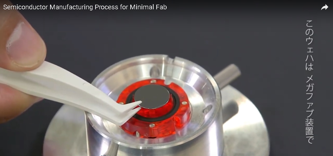
- the plate is located in a capsule isolated from the external environment (a certain analogue of SMIF), which opens only inside the unit. Only one plate is processed in one process.
(a container with a plate inside is loaded into the unit)

- all equipment is performed in a unified form factor (dimensions 1440x300x450mm), without a complicated start-up and connection procedure. Each unit performs one type of process (chemical treatment, etching, etc.).
The interface and control of installations is standardized.
No infrastructure is required in the usual MegaFactory format. Gases and reagents are located inside the units in compact cartridges (containers), gases in cylinders. A hood is required to remove the gaseous reaction products and heat sink:
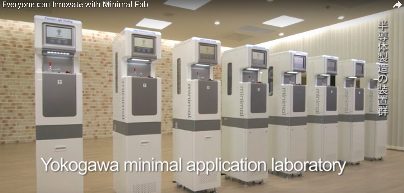
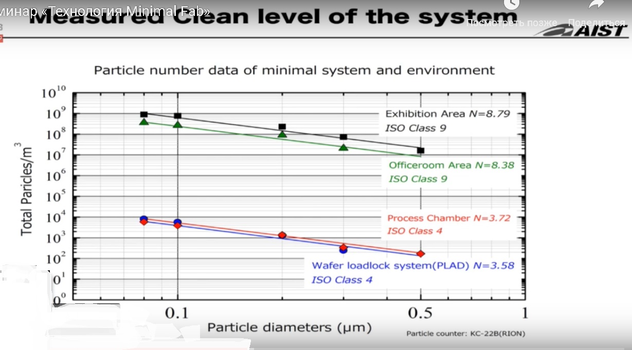
- it is declared that this does not require a clean room in the room, since the processing zone of the plate is isolated from the environment. Inside the plate processing area due to the tightness, a cleanliness class of ISO 4 is achieved (with an external cleanliness class in the room of ISO 9, a normal office).
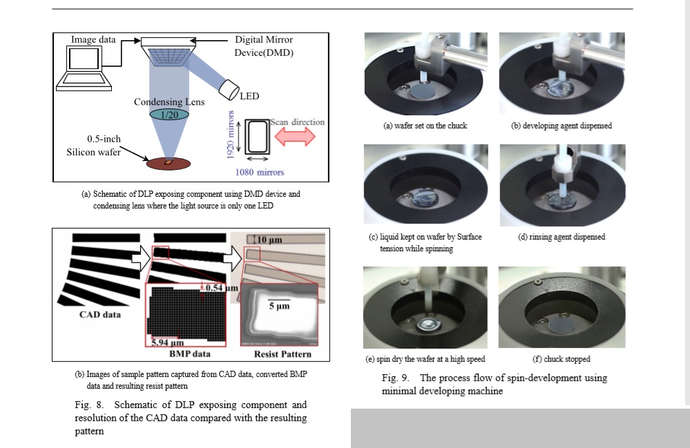
- maskless (without a photomask) method of forming a pattern on a plate. The image is formed due to direct projection onto a photoresist (classical application and development). The wavelength is 365 nm, the estimated resolution of the system is 0.5 μm. The edge zone is about 0.5 mm (the working diameter of the plate will be about 11 mm).

Obvious advantages of this concept:
The authors of the concept even give the following assessment, comparing MegaFab and Minimal Fab:

Very effective comparison. It is especially to the liking of those who insist that Minimal Fab replace a full-fledged factory, and this is the best and only way. Well, here there are billions, and here millions.
But this is where the clash of concept with reality begins.
To date, the level of implemented CMOS chips on the Minimal Fab line is not too amazing. Made very simple samples such as NAND-cells and ring generators, consisting of 400 transistors. The shutter size is a few microns, the technology is quite primitive (level of the late 70s, early 80s). In the photo, samples presented in 2018 at SEMI Japan.

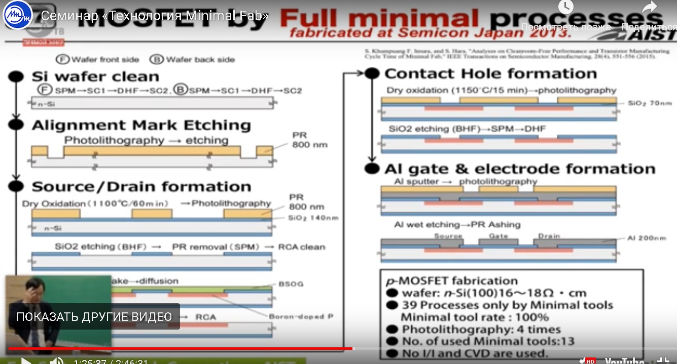
And also a slide from the presentation, which shows a schematic route for making samples in 2013. A route of 39 operations, pn junctions from a diffusion source, one layer of wiring ...
Ion doping processes are not currently implemented in the Miimal-Fab form factor, although work is ongoing. So far, energy has been promised up to 60 keV, and two types of elements, B and P. It is not clear how to achieve high energies in a limited size of installations. As an option - a hybrid implementation (do processes on conventional equipment, due to special holders).
Implementation of at least two-layer wiring, to talk about the level of 1-0.8 microns, is also not yet visible. Not all PCT processes have been implemented.
The level of photolithography reached today by the developers is named up to 0.5 microns. It is said that this seems to be a step, but some materials are not shown. Further in the plans is the transition to electron beam lithography, but this is in the future.
This is what the roadmap looks like:

So far, comparing a full-fledged factory worth five billion and the current Minimal Fab lineup looks somewhat misleading. And those who appeal to this do so either out of ignorance, or vice versa, because of too much knowledge.
The concept developer himself does not contrast himself with TSMC, for example.
A niche for the authors of the Miniaml Fab is seen. The figure shows an analysis of US semiconductor manufacturers (slide from the 2017 presentation).

Approximately 98 factories in the United States are manufacturing semiconductors in the process range from 0.5 microns or more, wafer diameters from 100 and below. These are producers of medium and small volumes, most often. These are all types (CMOS, MEMS, discrete). By the level of technology, this already roughly corresponds to the capabilities of the Minimal Fab line, with the current level of ph \ l (even without an electron beam). There is a hardware problem for these factories. New equipment for this diameter is not available, and here the Minimal Fab format is very suitable. According to developers, to replace these capacities, thousands of lines of Minimal Fab are required.
In principle, a similar situation, but on a smaller scale, exists in our country. We also have enough old rulers that make small volumes using the technology of King Peas (different shaggy series of ten transistors according to horse standards, etc.).
The second interesting and really relevant niche is specific technologies.
SOI, MEMS, sensors, hybrid circuits (CMOS + sensor, such as bolometers) discrete, microwave, backend operations such as bumping, A3B5 connections ... All this is done on a small diameter, usually with small volumes. And here Minimal Fab wins over the traditional implementation (in the photo an example of the implementation of the MEMS structure).

To date, it has been announced that already 5-6 lines of Minimal Fab work as fully functional for customers. A representative of one of the companies spoke at the seminar and spoke about his application experience.
Typically, they use the Minimal Fab equipment in a hybrid format. That is, they have a traditional clean room with equipment for the Backend process (something like an interposer for bumping). And several units of Minimal Fab implements processes f \ l and chemical processing.
We have the idea of MinimalFab successively promoting MIET. Conducts seminars and meetings with technology developers (within the framework of the meeting, after the conference, an agreement was signed between NRU MIET, Tokyo Boeki (RUS) LLC (with 100% Japanese capital) and the Association of Universities that train personnel in the field of electronic industry).
There is a Russian-language website of Tokyo BOEKI Rus.
A couple of years ago, ADGEX very pathetic announced the "beginning of a new era in the world of microelectronics" , and threatened to start supplying "devices" manufactured at the Minimal Fab in 2018, but something went wrong.
As an option in a hybrid mode (Minimal Fab in a classic factory).
The previous big seminar took place there in 2017, and there is almost a three-hour recording on youtube. For a long time I wanted to write a big note on this topic, I collected a lot of material, and after this meeting I finally “matured”. Still, a live meeting with questions and answers is much more effective than studying articles. In addition, recently there have been several articles where this line is covered one-sidedly, in some kind of admired and not entirely adequate way of “admiration”. Let's figure it out ...
Reduction concept
The main ideologist of the Minimal Fab project is the Japanese scientist Shiro Hara. In the mid-2000s, he proposed a radical approach to reduce the cost of semiconductor production - to take the path of reducing equipment and the diameter of the original wafers.
In 2010, to implement this idea, a consortium was created with the support of the Government of Japan and under the auspices of the National Institute of Advanced Industrial Sciences and Technologies (AIST). This consortium includes more than a hundred Japanese companies involved in the development of materials, equipment and technologies.
In 2017, a separate organization was allocated to promote Minimal Fab as a ready-made solution to the semiconductor market (Tokyo Boeki Group Ltd).
This idea of reduction goes against the current global trend. If you look at the modern evolution of semiconductor manufacturing, then along with a decrease in the minimum size, an increase in the diameter of the plates and an increase in the productivity of the equipment occur. This leads to the fact that several leading companies, such as TSMC, Intel, Samsung, can pull the creation of modern mass production today. These are the owners of the so-called MegaFabs, in terms of the concept.
They “hold” more than half of the total market, possessing significant production capacities for the production of mass IP. Small producers are being “washed out” of the market, unable to compete in price with giants in the consumer sector. Or go into specific niches of unique products, with a large margin, but with small volumes. At the same time, small companies are in an unstable position, as they are forced to follow the global trend of "gigantomania" and invest heavily in infrastructure and equipment. Conventionally, if I want to build a line today for a small volume, and the old level of technology (~ 3 μm), then I will have to spend more than it was thirty years ago at equivalent prices. Such is the paradox.
What to do for those who want to buy a small series of IP? You can go to the same giant companies and order a shuttle from them, as part of the MWP. It will not be very cheap and not too fast (manufacturing cycle 1-2 months in CMOS technology 28nm). But if you need something specific in terms of technology, then there will be a problem. The development of technology is very expensive, and no one will do it to complete an order, for example, for ten plates. It would be nice to have your own ruler, but not expensive.)
The author of the Minimal Fab concept proposed to significantly reduce the cost of the “entrance ticket” to the production of semiconductors. This is achieved by the following solutions:
- reducing the diameter of the plates from the modern standard 300mm (plate area ~ 70650mm2) to a diameter of 12.5mm (plate area ~ 122mm2). This area is enough to accommodate one large scheme or several small ones. The plates are made by “clipping” from large plates, with additional processing (photo of the plate placed in the cassette):
- the plate is located in a capsule isolated from the external environment (a certain analogue of SMIF), which opens only inside the unit. Only one plate is processed in one process.
(a container with a plate inside is loaded into the unit)
- all equipment is performed in a unified form factor (dimensions 1440x300x450mm), without a complicated start-up and connection procedure. Each unit performs one type of process (chemical treatment, etching, etc.).
The interface and control of installations is standardized.
No infrastructure is required in the usual MegaFactory format. Gases and reagents are located inside the units in compact cartridges (containers), gases in cylinders. A hood is required to remove the gaseous reaction products and heat sink:
- it is declared that this does not require a clean room in the room, since the processing zone of the plate is isolated from the environment. Inside the plate processing area due to the tightness, a cleanliness class of ISO 4 is achieved (with an external cleanliness class in the room of ISO 9, a normal office).
- maskless (without a photomask) method of forming a pattern on a plate. The image is formed due to direct projection onto a photoresist (classical application and development). The wavelength is 365 nm, the estimated resolution of the system is 0.5 μm. The edge zone is about 0.5 mm (the working diameter of the plate will be about 11 mm).
Obvious advantages of this concept:
- reduction of initial costs for the organization of production by tens or hundreds of times
- no need to build a capital building with supporting infrastructure
- reducing the cost of maintaining the operation of such a line by tens or hundreds of times in relation to a conventional line (by reducing the consumption of electricity, materials, reducing staff by standardizing equipment)
- Significantly faster sample production times (from a few weeks to days)
- a hybrid option is possible, when some operations, subject to adaptation, can be performed on standard "large" equipment (IL, f \ l).
- production of photo masks is not required, image correction is possible if necessary
The authors of the concept even give the following assessment, comparing MegaFab and Minimal Fab:
Very effective comparison. It is especially to the liking of those who insist that Minimal Fab replace a full-fledged factory, and this is the best and only way. Well, here there are billions, and here millions.
But this is where the clash of concept with reality begins.
Reality
To date, the level of implemented CMOS chips on the Minimal Fab line is not too amazing. Made very simple samples such as NAND-cells and ring generators, consisting of 400 transistors. The shutter size is a few microns, the technology is quite primitive (level of the late 70s, early 80s). In the photo, samples presented in 2018 at SEMI Japan.
And also a slide from the presentation, which shows a schematic route for making samples in 2013. A route of 39 operations, pn junctions from a diffusion source, one layer of wiring ...
Ion doping processes are not currently implemented in the Miimal-Fab form factor, although work is ongoing. So far, energy has been promised up to 60 keV, and two types of elements, B and P. It is not clear how to achieve high energies in a limited size of installations. As an option - a hybrid implementation (do processes on conventional equipment, due to special holders).
Implementation of at least two-layer wiring, to talk about the level of 1-0.8 microns, is also not yet visible. Not all PCT processes have been implemented.
The level of photolithography reached today by the developers is named up to 0.5 microns. It is said that this seems to be a step, but some materials are not shown. Further in the plans is the transition to electron beam lithography, but this is in the future.
This is what the roadmap looks like:
So far, comparing a full-fledged factory worth five billion and the current Minimal Fab lineup looks somewhat misleading. And those who appeal to this do so either out of ignorance, or vice versa, because of too much knowledge.
The concept developer himself does not contrast himself with TSMC, for example.
A niche for the authors of the Miniaml Fab is seen. The figure shows an analysis of US semiconductor manufacturers (slide from the 2017 presentation).
Approximately 98 factories in the United States are manufacturing semiconductors in the process range from 0.5 microns or more, wafer diameters from 100 and below. These are producers of medium and small volumes, most often. These are all types (CMOS, MEMS, discrete). By the level of technology, this already roughly corresponds to the capabilities of the Minimal Fab line, with the current level of ph \ l (even without an electron beam). There is a hardware problem for these factories. New equipment for this diameter is not available, and here the Minimal Fab format is very suitable. According to developers, to replace these capacities, thousands of lines of Minimal Fab are required.
In principle, a similar situation, but on a smaller scale, exists in our country. We also have enough old rulers that make small volumes using the technology of King Peas (different shaggy series of ten transistors according to horse standards, etc.).
The second interesting and really relevant niche is specific technologies.
SOI, MEMS, sensors, hybrid circuits (CMOS + sensor, such as bolometers) discrete, microwave, backend operations such as bumping, A3B5 connections ... All this is done on a small diameter, usually with small volumes. And here Minimal Fab wins over the traditional implementation (in the photo an example of the implementation of the MEMS structure).
To date, it has been announced that already 5-6 lines of Minimal Fab work as fully functional for customers. A representative of one of the companies spoke at the seminar and spoke about his application experience.
Typically, they use the Minimal Fab equipment in a hybrid format. That is, they have a traditional clean room with equipment for the Backend process (something like an interposer for bumping). And several units of Minimal Fab implements processes f \ l and chemical processing.
Promotion with us
We have the idea of MinimalFab successively promoting MIET. Conducts seminars and meetings with technology developers (within the framework of the meeting, after the conference, an agreement was signed between NRU MIET, Tokyo Boeki (RUS) LLC (with 100% Japanese capital) and the Association of Universities that train personnel in the field of electronic industry).
There is a Russian-language website of Tokyo BOEKI Rus.
A couple of years ago, ADGEX very pathetic announced the "beginning of a new era in the world of microelectronics" , and threatened to start supplying "devices" manufactured at the Minimal Fab in 2018, but something went wrong.
Summing up the personal outcome
- Minimal Fab format is not just a simulator for student learning (although, I admit, a couple of years ago I thought it was more like that)
- Ideal for MEMS, sensors, sensors, bolometers, etc.
- suitable for discrete devices, microwave, power electronics and specific materials, such as SOI, A3B5. (possibly in a hybrid implementation)
- a very realistic option for the manufacture of bipolar or CMOS circuits of the level of 3 μm and higher, with a small degree of integration (for example, numerous
militaryseries, of ten transistors and three resistors with horse sizes, which are still forged) - promisingly for replacing outdated rulers of small diameter plates and for a small series (a problem of old equipment that no one physically does)
- extremely interesting is the implementation of packaging \ bumping \ interposers and so on (in the case of a small series)
- CMOS level from 0.5 microns to 0.25 microns - possibly in the future, depends on investments in technology.
As an option in a hybrid mode (Minimal Fab in a classic factory).
- for a full-fledged CMOS and a large degree of integration (below 0.25 μm), there are few prerequisites, even if there is electron-beam f \ l. Still, the size in the naked form is far from everything. Below 0.25 microns, the technical process is much more complicated, and most importantly, the design component.
- below 0.18mkm - developers don’t even see plans in the near future
- large factories with nodes 28nm and lower can sleep peacefully, Minimal Fab is not a competitor to them in the foreseeable future.
Minimal Fab Materials and Resources
- Recording of a large seminar at MIET, 2017.
- The video about the manufacturing process is very clear.
- Presentation of SEMI EXPO Moscow 2017