KeeBee Making your own USB keyboard from scratch
- Transfer
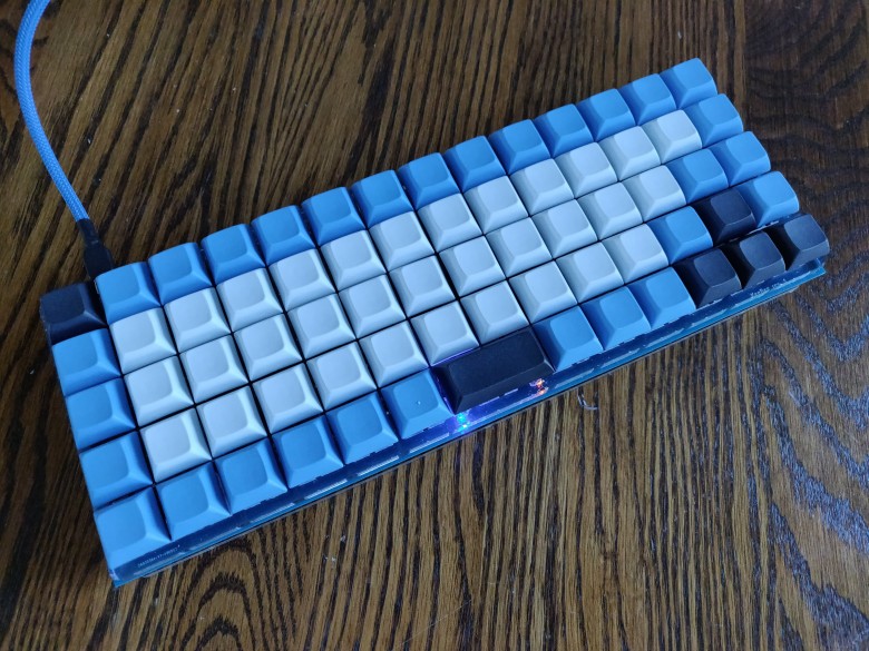
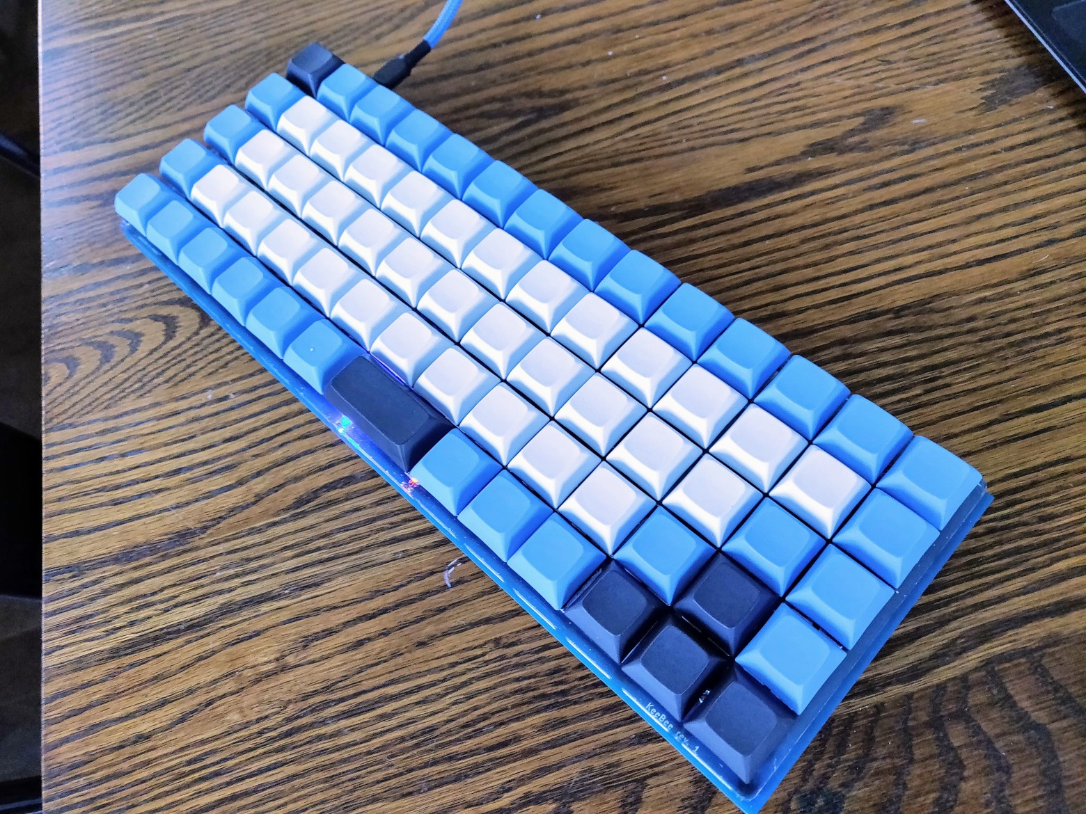
A few months ago, my project for manufacturing a USB keyboard was completed. Among other things, I completed the design of electronic circuits, designed a printed circuit board, programmed the firmware, made a layout in CAD and assembled the device. The result is a comfortable keyboard, which I use daily and affectionately call KeeBee: KeeBee keyboard in its final form.
Several goals of the project:
At work, I mainly develop software for cloud services, where many layers of real equipment are missing. Therefore, it is very nice to get rid of some abstractions and go down to the hardware level: here are real electronic devices that you can touch and use.
I really like the minimalistic OLKB Planck and Preonic style keyboards , which, due to the ortho-linear arrangement of the keys, are very compact. I also knew right away that I wanted to use the Cherry MX Brown switches. With these two design components in mind, I started playing with key layouts in OpenSCAD . This is a great open source tool that works more like a programming language than a WYSIWYG mouse interface.
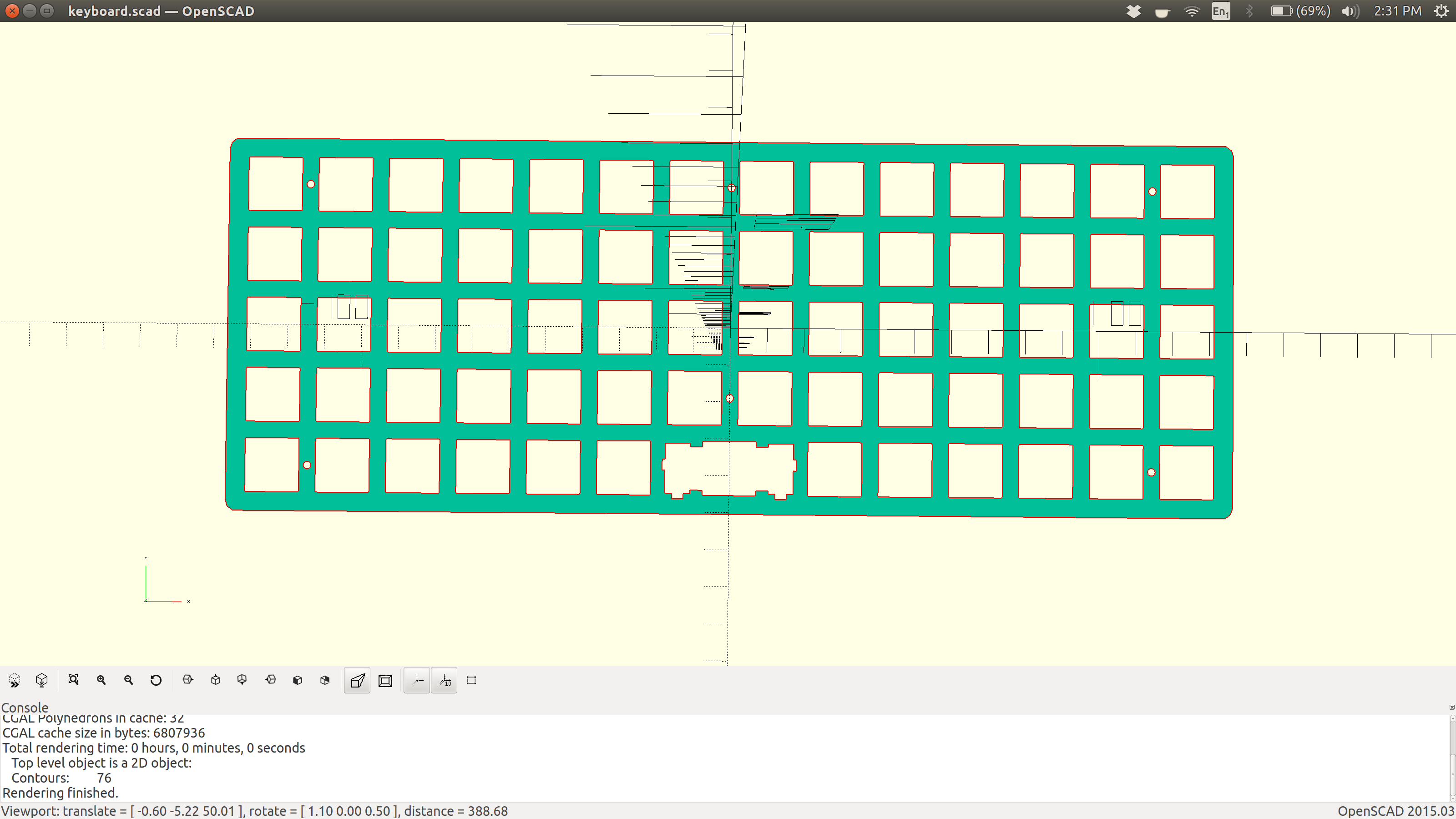
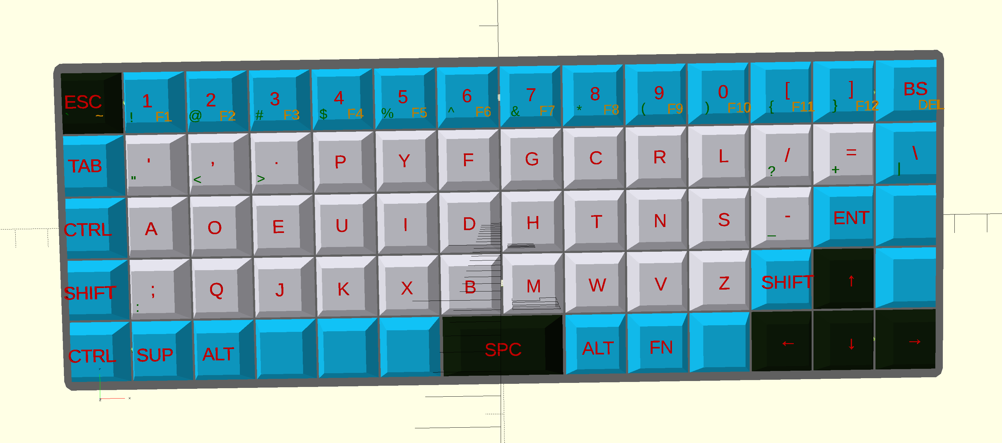
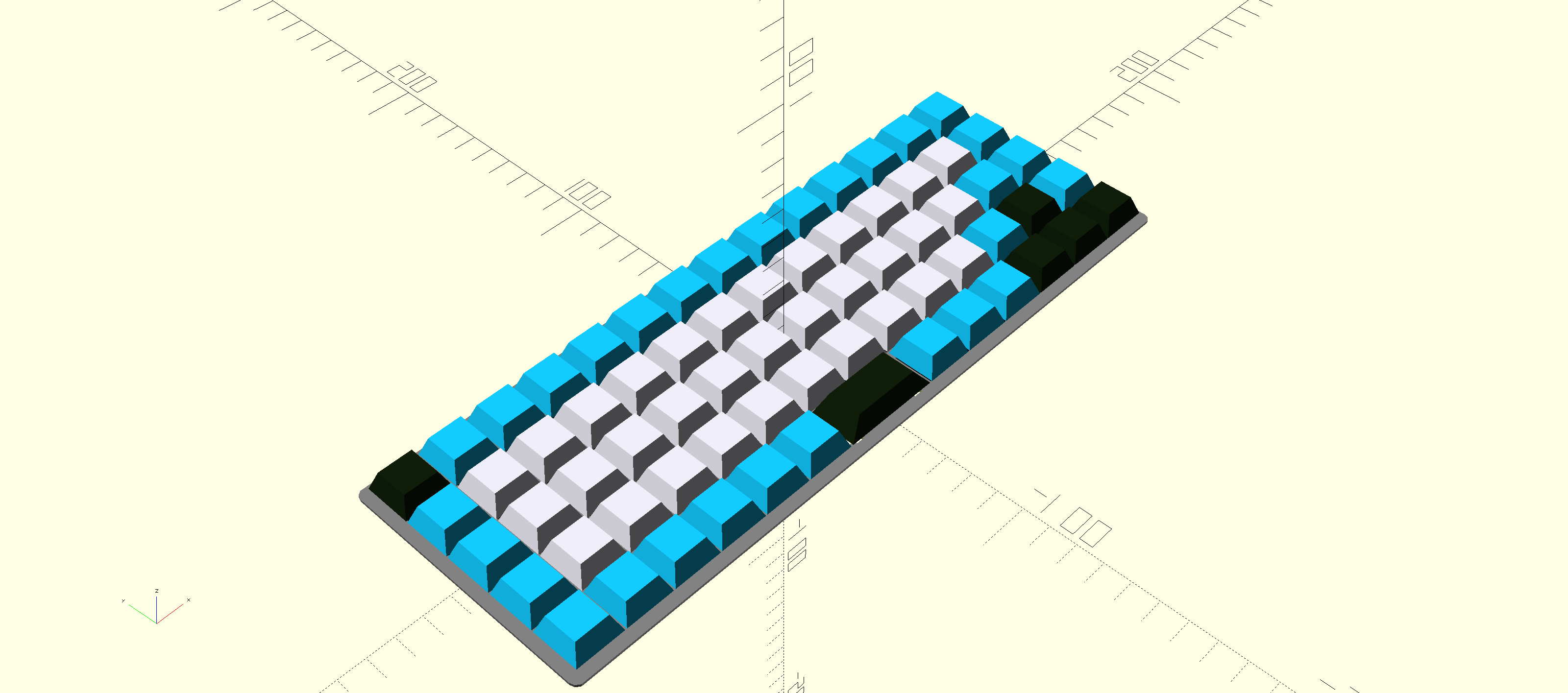
Taking the sizes of the elements from the Cherry MX documentation, I made the layout of the top plate, then added switches and keys to get an idea of what the final result would look like. The top plate is located above the keyboard PCB and serves as a good stabilizer for the switches.
Top plate design:
After adding keys:
As the main microcontroller, I chose STM32F042K6T6 . This is about three dollars per chip, if you take from one piece. He has enough contacts for the scanning matrix of 69 keys (32 contacts in total). It runs on an ARM Cortex M0 processor and contains special USB peripherals for sending a USB signal without loading the main processor with this task. I bought a Nucleo prototype dev board with this chip before integrating it into my PCB design. Nucleo very conveniently lay on a breadboard and powered via USB.
I placed a small four-key circuit on the breadboard to test the diode circuitwhich I studied. Ignoring the USB side of the equation, the first step was to make the Cherry switches reliably turn on and off the four corresponding LEDs when the buttons were pressed.
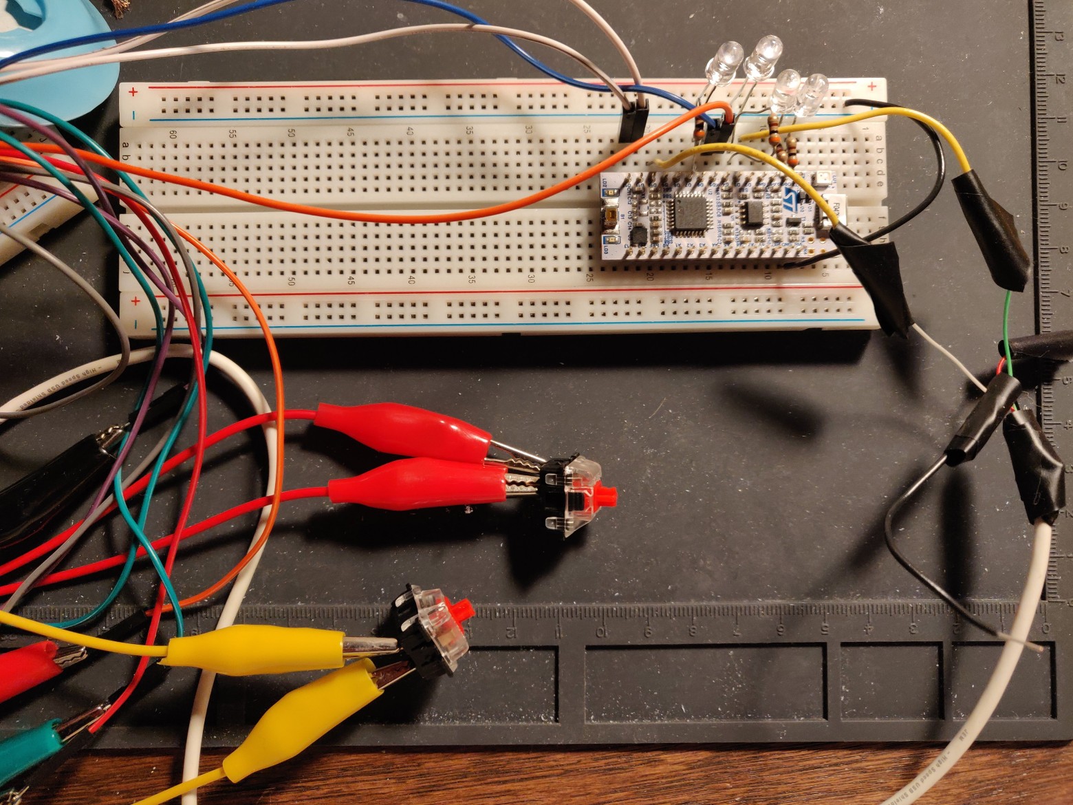
The scanning matrix is such a technique that you need to use when you have more switches than contacts on the microcontroller.
When the matrix worked satisfactorily , it was time to work on USB.
The built-in firmware cycle is essentially this:
From main.cc :
The component
Having tinkered for a while, I still made the four-key keyboard correctly identify itself as a USB HID (Human Interface Device) and all the presses were correctly transferred to the laptop:

Registering as a USB vendor and getting an official device id is expensive . If you just have an amateur project, then you have to grab the identifier of some similar device . I thought that “Gear Head” sounds cool, especially since they release keyboards, so I chose them.

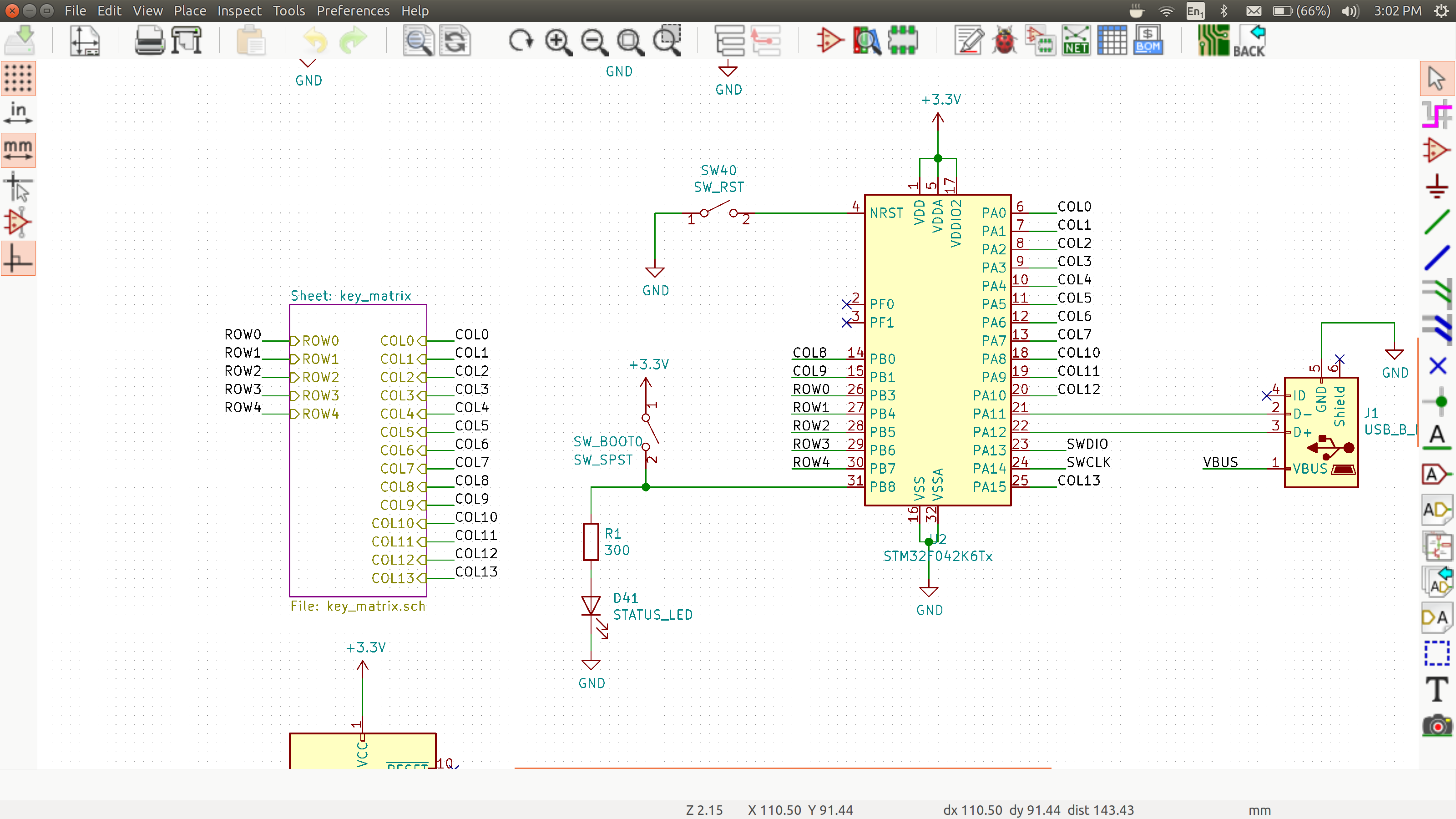
Having received more or less working firmware and a working prototype, it's time to draw up the circuit and design of the circuit board in KiCAD and make a real circuit board. When I made sure that the circuit for 4 buttons works, the relatively simple task of connecting everything together remained:
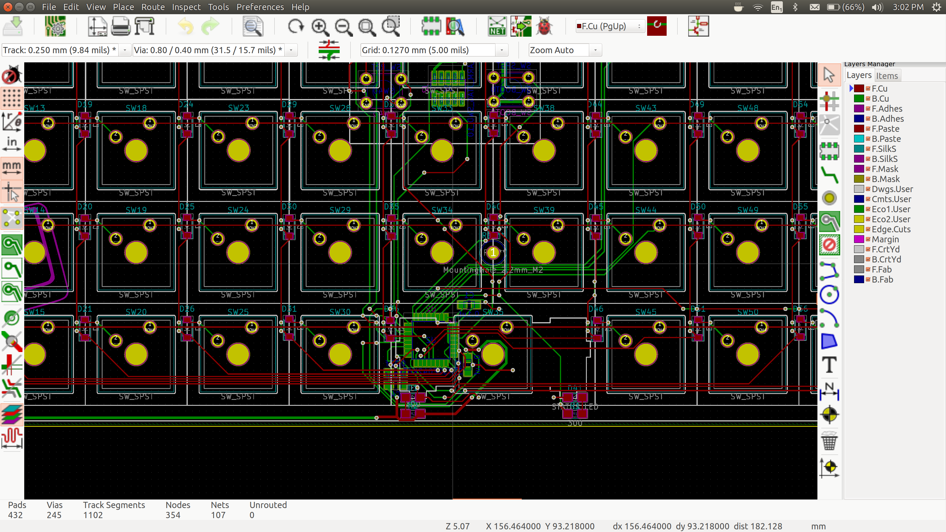
After designing the circuit and setting up the pads for the components, you need to make a real PCB layout:
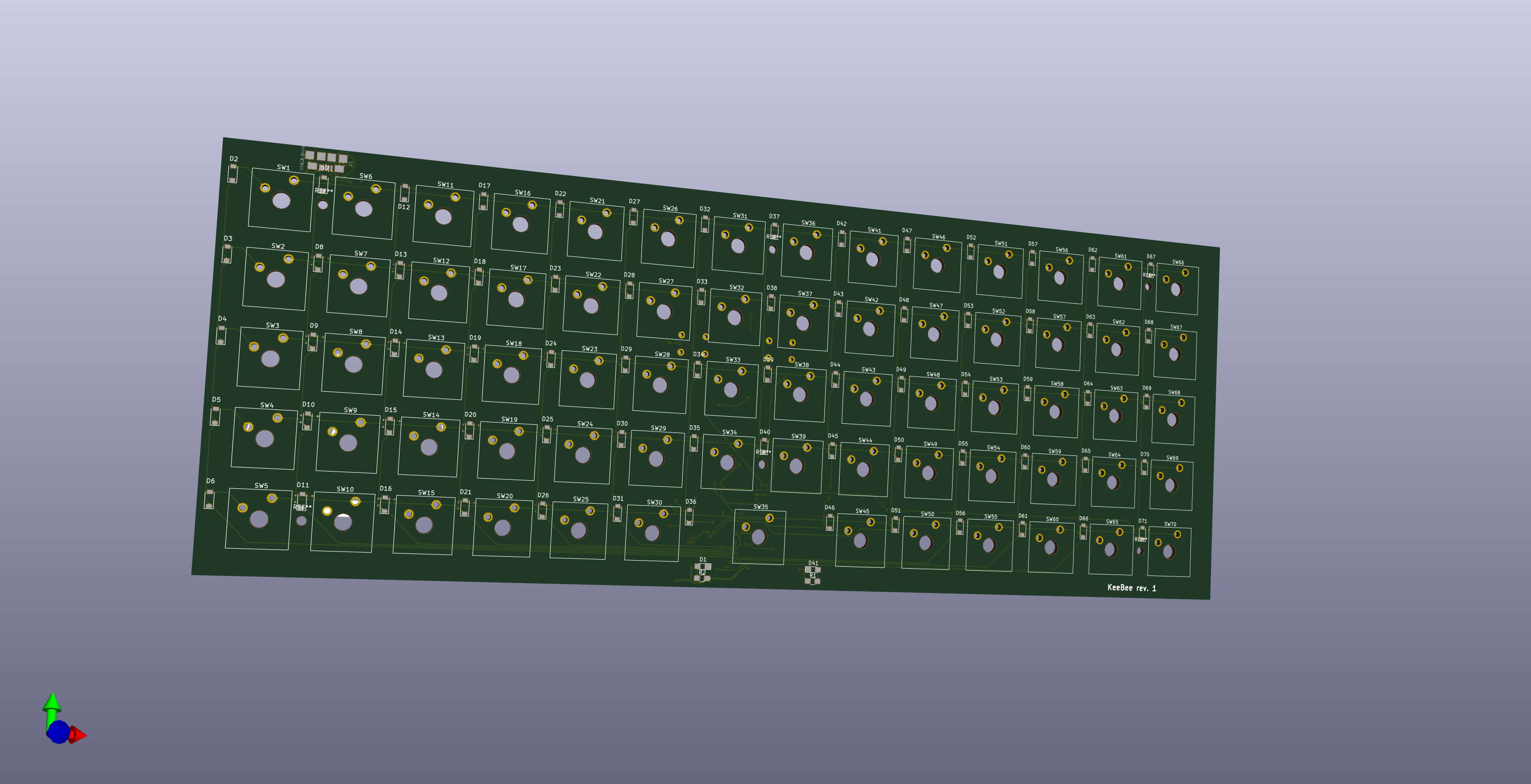
KiCAD can beautifully render the future circuit board in 3D:
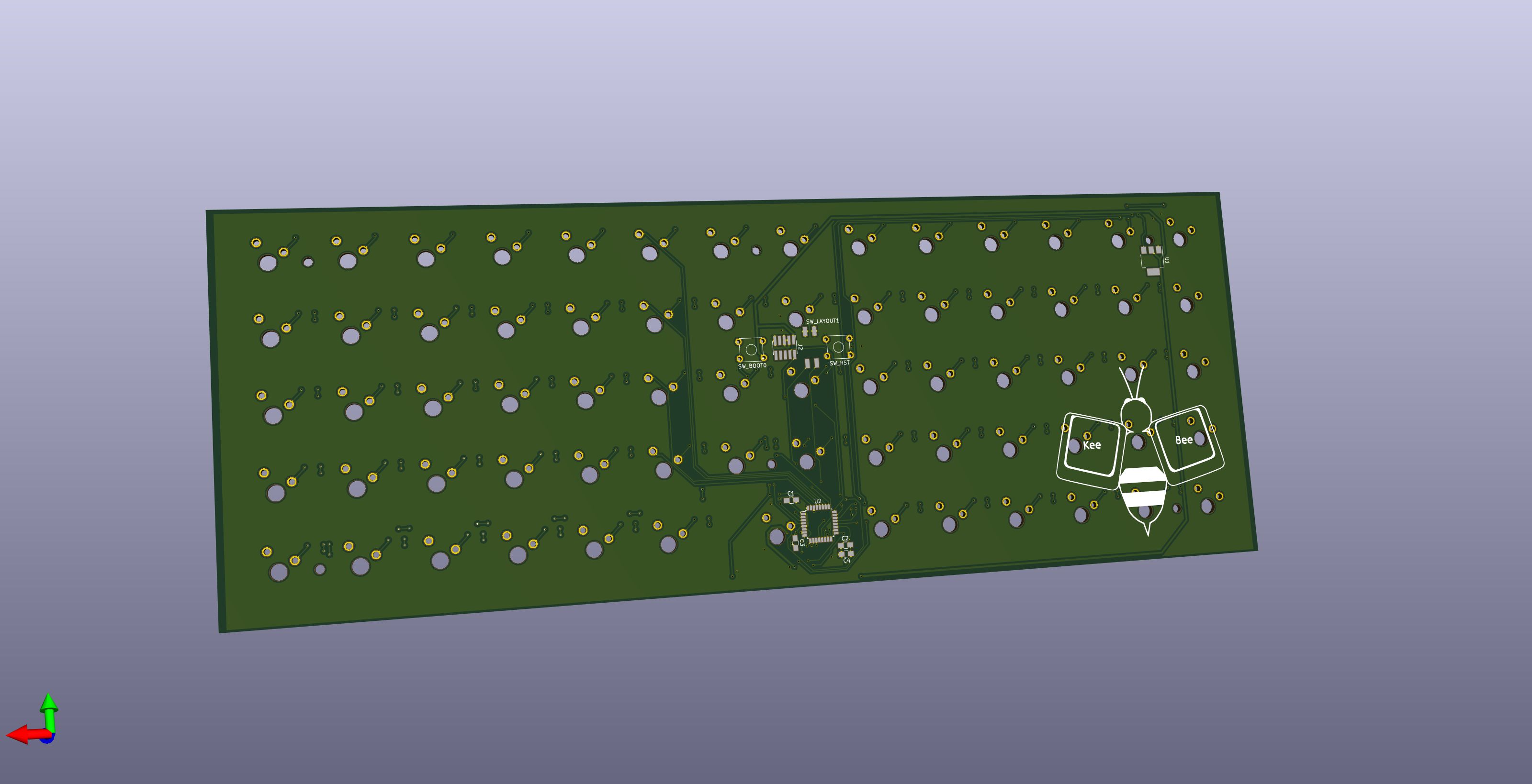
There are many great KiCAD tutorials. I started with the excellent Getting to Blinkey 4.0 video series from Chris Gammel, where he explains in detail all the steps involved in creating a LED linker circuit in KiCAD from start to finish.
Having brought the circuit board design and design to a satisfactory level, I began to place a bunch of orders:
The day the package arrived is the best:
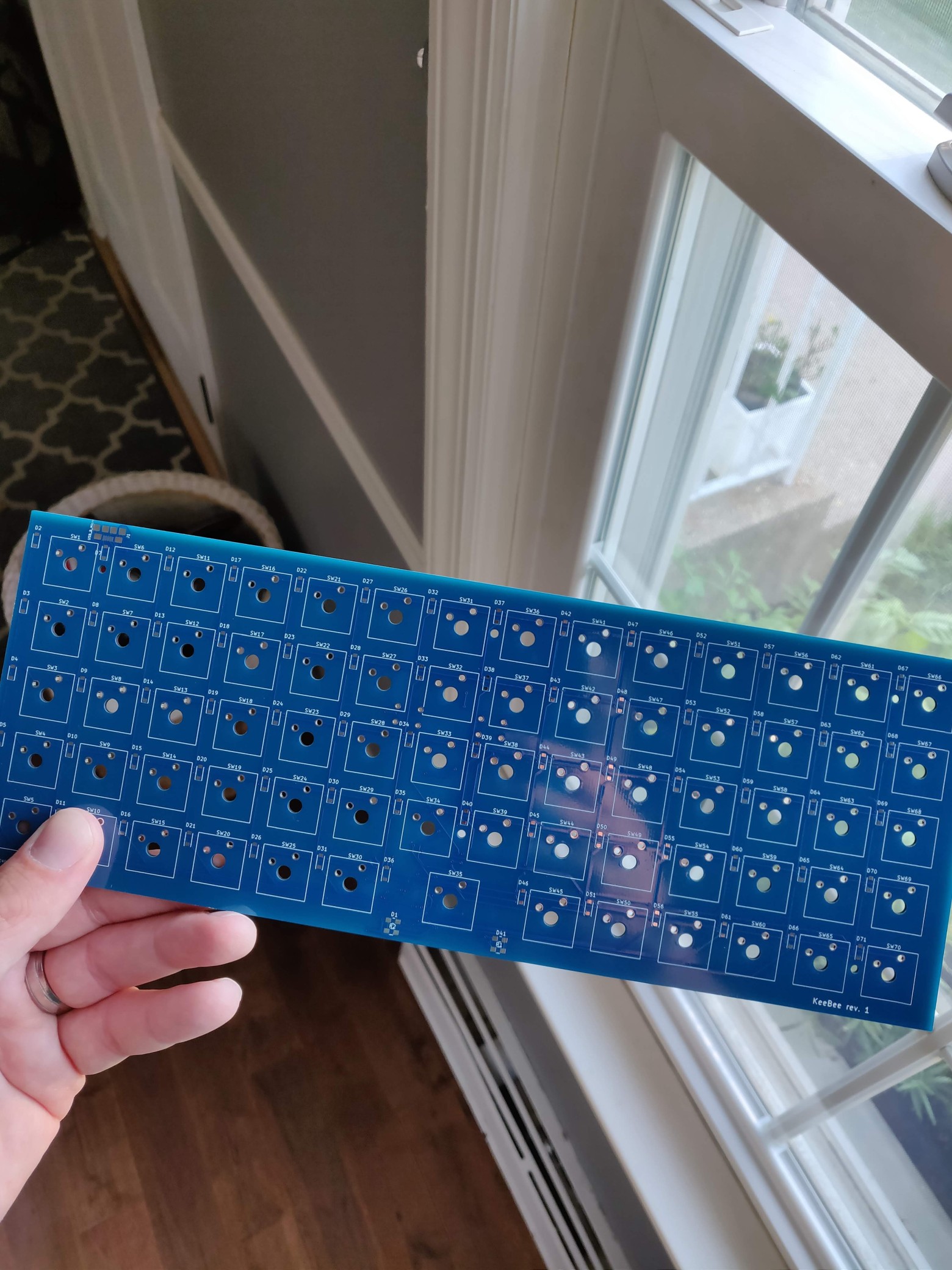
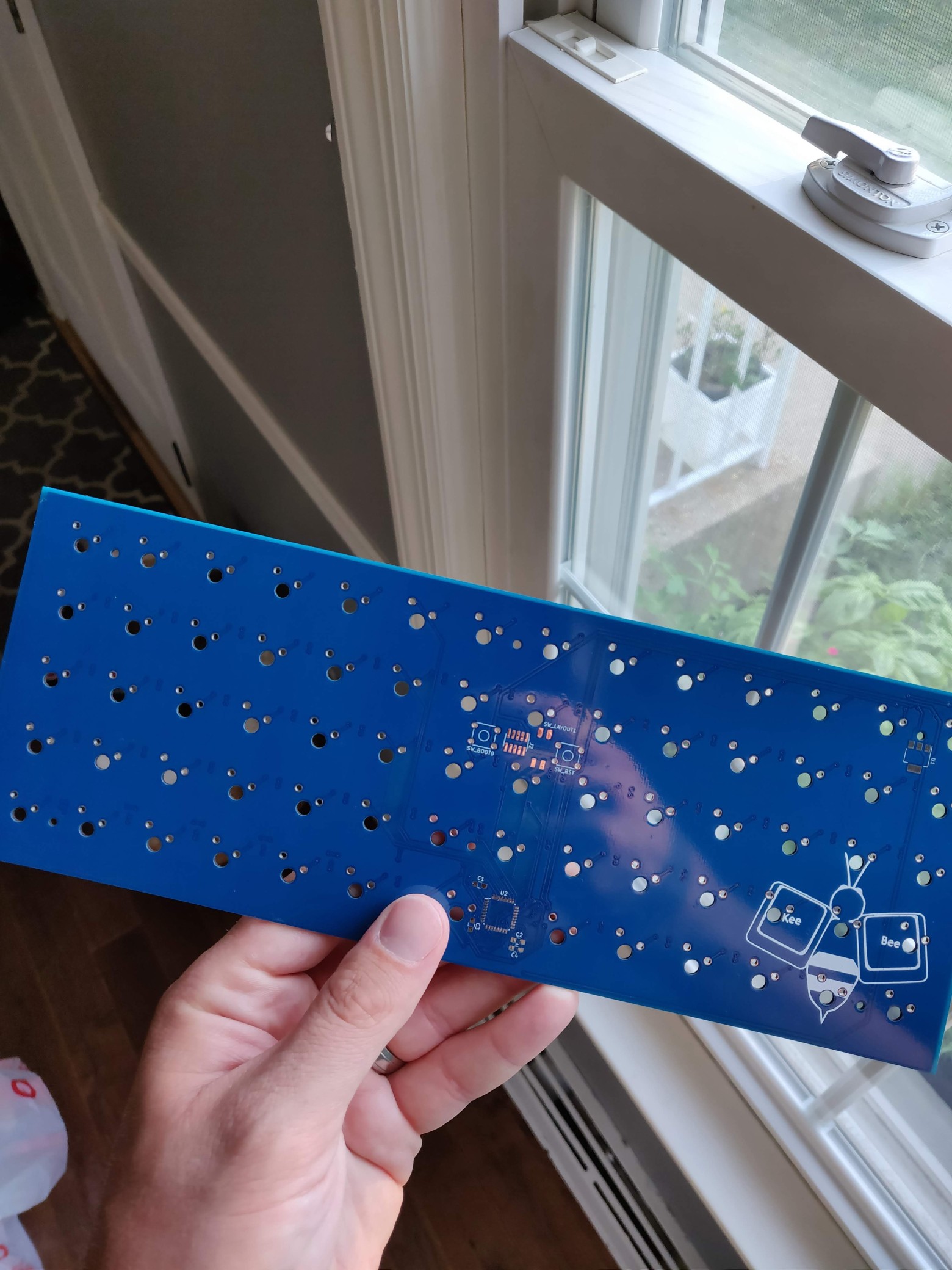
JLCPCB is a very affordable service. This design with DHL delivery from China cost less than $ 30, and the whole process from downloading files to the arrival of the parcel took a little more than a week.
Shurin took the DXF files from OpenSCAD and threw them into the laser cutter:

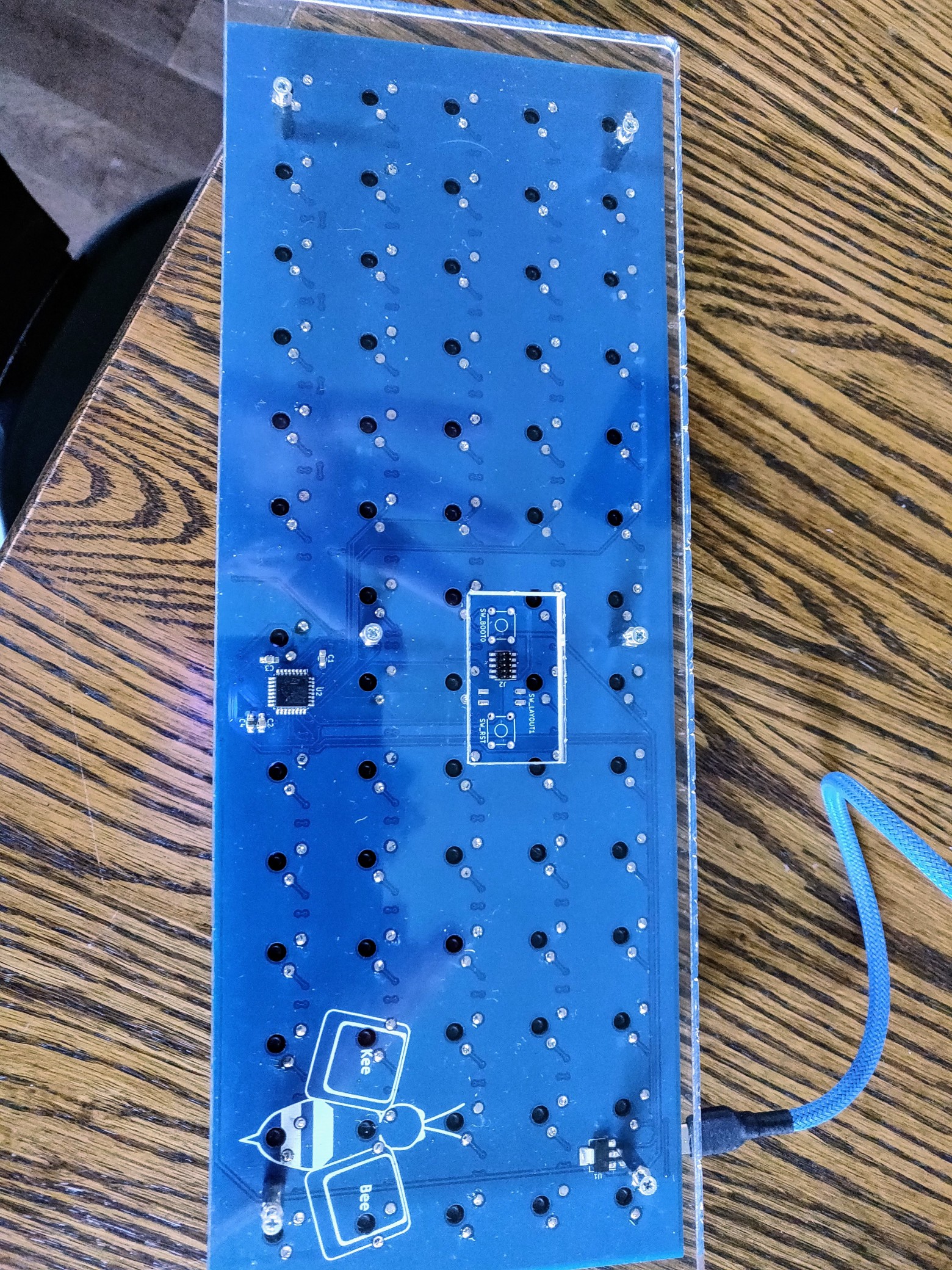
Having received all the details, I started assembling. The first step is to assemble the components of the circuit board: a soldering iron for large electronic components and a soldering station for surface mounting of small components, such as the STM32 microcontroller.
The total assembly time of the board was about three hours - most of it was soldering 70 diodes and switches.
I added a header for JTAG debugging, through which I connected JLINK Edu mini for microcontroller firmware using OpenOCD .
Then the time came for the final testing and final assembly:
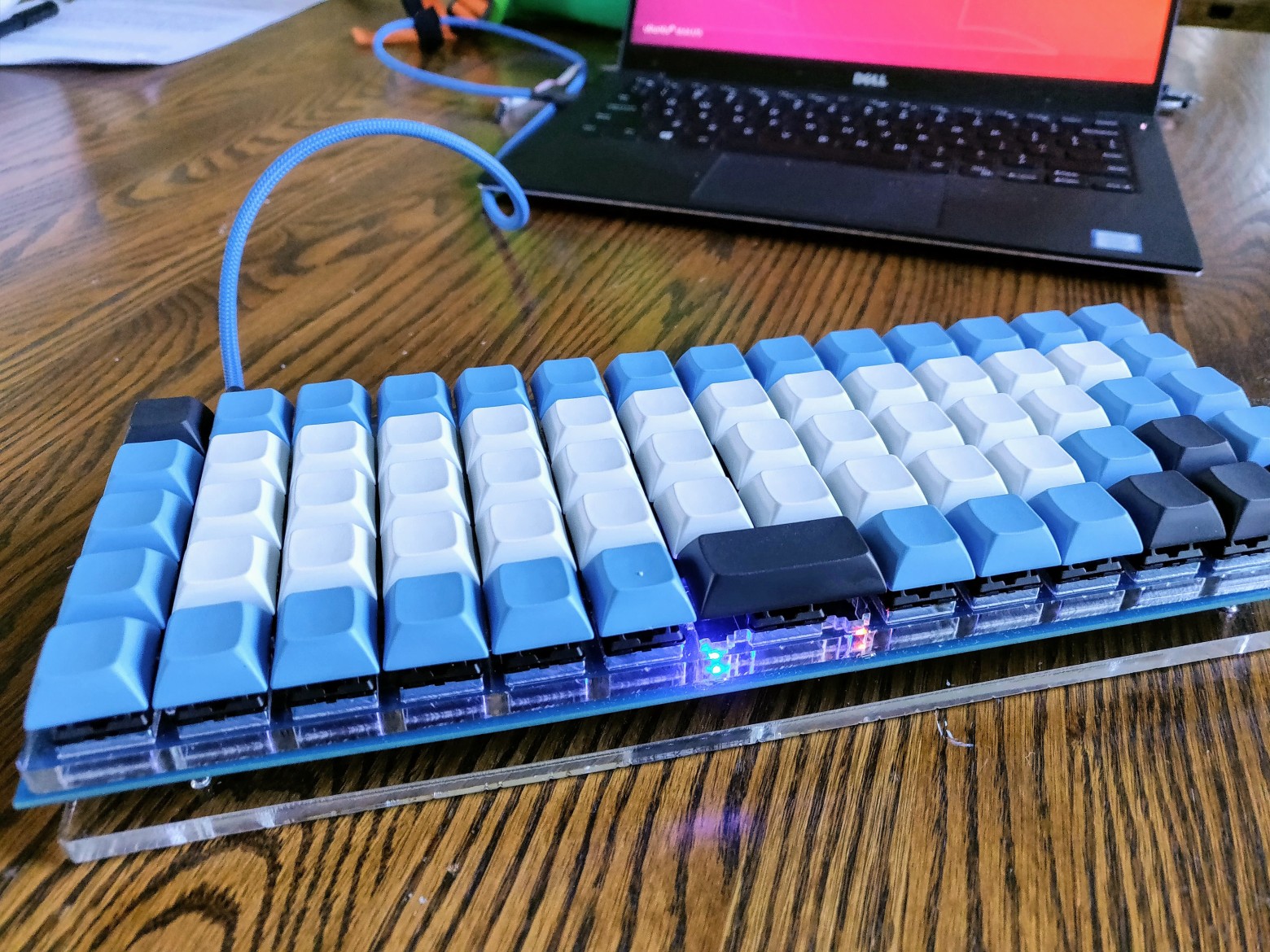
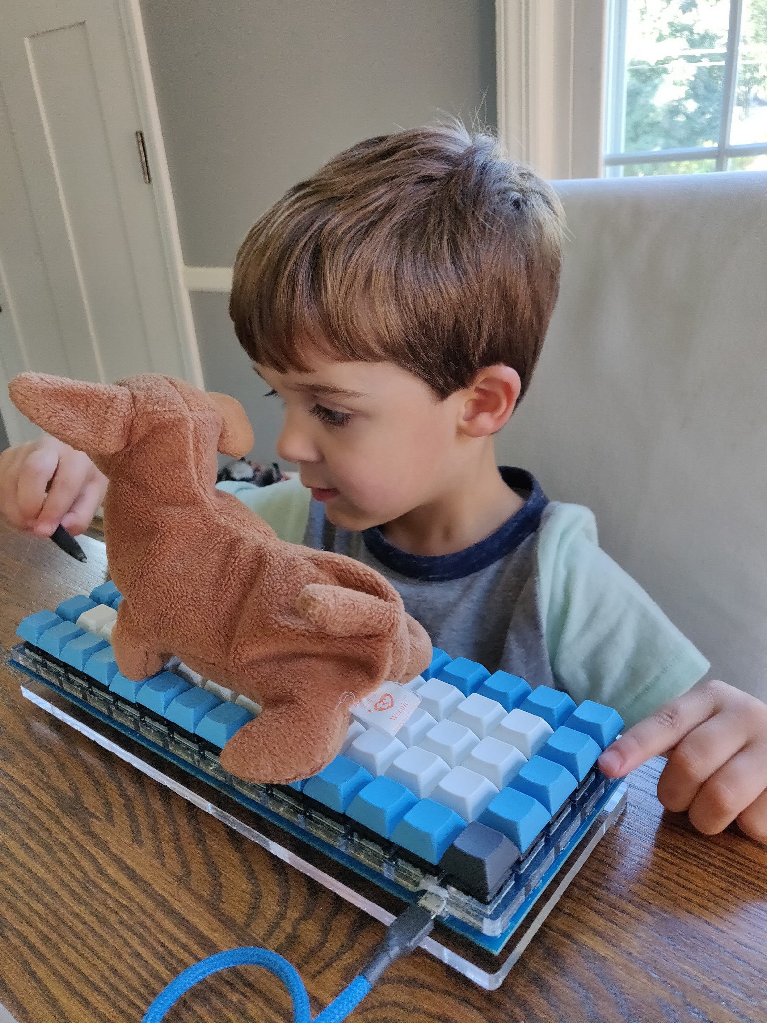
The son decided that this was a great train for his animals:

From the initial idea to the final assembly, the project took about three months. It was extremely useful as a hobby to do what I still use every day at work.
All project files are published on GitHub , including firmware sources, circuit boards, a list of materials and CAD models.
Thanks for reading and enjoy the hacks!

- Self-creation of the scheme.
- Writing keyboard firmware.
- Learn how the USB protocol works.
At work, I mainly develop software for cloud services, where many layers of real equipment are missing. Therefore, it is very nice to get rid of some abstractions and go down to the hardware level: here are real electronic devices that you can touch and use.
Study and CAD layout
I really like the minimalistic OLKB Planck and Preonic style keyboards , which, due to the ortho-linear arrangement of the keys, are very compact. I also knew right away that I wanted to use the Cherry MX Brown switches. With these two design components in mind, I started playing with key layouts in OpenSCAD . This is a great open source tool that works more like a programming language than a WYSIWYG mouse interface.
Taking the sizes of the elements from the Cherry MX documentation, I made the layout of the top plate, then added switches and keys to get an idea of what the final result would look like. The top plate is located above the keyboard PCB and serves as a good stabilizer for the switches.
Top plate design:

After adding keys:


Board prototyping and firmware design
As the main microcontroller, I chose STM32F042K6T6 . This is about three dollars per chip, if you take from one piece. He has enough contacts for the scanning matrix of 69 keys (32 contacts in total). It runs on an ARM Cortex M0 processor and contains special USB peripherals for sending a USB signal without loading the main processor with this task. I bought a Nucleo prototype dev board with this chip before integrating it into my PCB design. Nucleo very conveniently lay on a breadboard and powered via USB.
I placed a small four-key circuit on the breadboard to test the diode circuitwhich I studied. Ignoring the USB side of the equation, the first step was to make the Cherry switches reliably turn on and off the four corresponding LEDs when the buttons were pressed.

The scanning matrix is such a technique that you need to use when you have more switches than contacts on the microcontroller.
When the matrix worked satisfactorily , it was time to work on USB.
The built-in firmware cycle is essentially this:
- Scan all the keys in the matrix.
- Match the button layout to the corresponding characters in the selected layout (QWERTY, Dvorak, etc.).
- Take the result of the comparison, generate USB HID Report packets and send it to the USB peripheral device.
- Turn on the LED on the keyboard, if the key is pressed, turn off - if not.
From main.cc :
static void scan_and_update() {
    scan_matrix.Scan(key_scans, row_count, column_count);
    keyboard.SendReport(
        key_pipeline.MapKeyScans(key_scans, key_count));
    update_key_press_status();
}
int main() {
    Init();
    status_led.SetOk(true);
    while (true) {
        scan_and_update();
    }
}
The component
keyboard.SendReportactually transfers the packets to the USB host. I tried hard to get USB to work properly. There are many non-trivial layers in this protocol that require accurate timing and proper identification of the device . In the end, I had to run Wireshark to listen to all the USB packets coming into my Linux laptop and find out where that got lost. A search on the Internet yielded almost nothing, most of the questions are answered approximately like this: “Probably your USB device has broken, you need to buy a new one.” If you are actually trying to design a USB device, these answers are not very helpful. I could only plunge into the voluminous USB specifications with a lot of unfamiliar terminology.Having tinkered for a while, I still made the four-key keyboard correctly identify itself as a USB HID (Human Interface Device) and all the presses were correctly transferred to the laptop:

Registering as a USB vendor and getting an official device id is expensive . If you just have an amateur project, then you have to grab the identifier of some similar device . I thought that “Gear Head” sounds cool, especially since they release keyboards, so I chose them.

Circuit and PCB
Having received more or less working firmware and a working prototype, it's time to draw up the circuit and design of the circuit board in KiCAD and make a real circuit board. When I made sure that the circuit for 4 buttons works, the relatively simple task of connecting everything together remained:

After designing the circuit and setting up the pads for the components, you need to make a real PCB layout:

KiCAD can beautifully render the future circuit board in 3D:


There are many great KiCAD tutorials. I started with the excellent Getting to Blinkey 4.0 video series from Chris Gammel, where he explains in detail all the steps involved in creating a LED linker circuit in KiCAD from start to finish.
Order PCB and components
Having brought the circuit board design and design to a satisfactory level, I began to place a bunch of orders:
- All components from the list of materials : switches, LEDs, diodes, microcontrollers, etc. I usually order these things on DigiKey .
- The circuit board itself. Quite a lot of services are ready to inexpensively make you a prototype. I have excellent experience with OshPark and JLCPCB . For this project, I chose JLCPCB because of the price for such a size, and also because they allowed me to choose a blue coating.
- All other details: covers and stuff. For this project, my brother-in-law helped laser cut the upper and lower keyboard plates from 1/4 ”acrylic sheets. For the remaining parts, you can use the online laser cutting and 3D printing services if you do not have access to the equipment.
The day the package arrived is the best:


JLCPCB is a very affordable service. This design with DHL delivery from China cost less than $ 30, and the whole process from downloading files to the arrival of the parcel took a little more than a week.
Shurin took the DXF files from OpenSCAD and threw them into the laser cutter:

Final assembly
Having received all the details, I started assembling. The first step is to assemble the components of the circuit board: a soldering iron for large electronic components and a soldering station for surface mounting of small components, such as the STM32 microcontroller.
The total assembly time of the board was about three hours - most of it was soldering 70 diodes and switches.
I added a header for JTAG debugging, through which I connected JLINK Edu mini for microcontroller firmware using OpenOCD .
Then the time came for the final testing and final assembly:


The son decided that this was a great train for his animals:


Summary
From the initial idea to the final assembly, the project took about three months. It was extremely useful as a hobby to do what I still use every day at work.
All project files are published on GitHub , including firmware sources, circuit boards, a list of materials and CAD models.
Thanks for reading and enjoy the hacks!
