3D microchip 1000 times faster than existing ones
Scientists have invented a new method for the development and creation of computer microchips, which can significantly accelerate data processing by at least 1000 times compared to existing CPUs. This method is based on a material called carbon nanotubes and allows you to build a microchip in three dimensions.
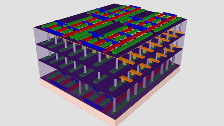
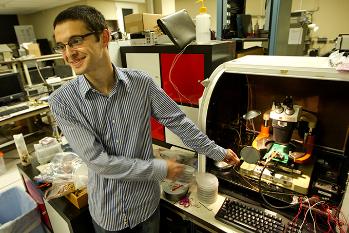
According to Max Shulaker, a member of the chip design team and a Ph.D. candidate in electrical engineering at Stanford University of California, such a 3D project significantly saves space in the system and increases the speed of data processing. This is achieved due to the fact that scientists contain a memory that stores all the data and compact the number of processors in a miniature space.
Reducing the distance between two elements can significantly speed up the processing time of commands by a computer.

Photo by Max Schalaker.
Computational capabilities of computer systems over the past 50 years have been constantly improved. This is largely due to the ability to continuously reduce silicon transistors and three-way switches with which logical operations are performed.
According to Moore's Law, a gross rule formulated by Gordon E. Moore in 1965, the number of silicon transistors on a chip must double every two years. Which is true, to further follow the rule, you need to reduce tiny silicon transistors to 5 nanometers. But here a problem arises - the limit for silicon, which is 7 nanometers (for comparison, the size of a human hair is on average about 100,000 nanometers). Subsequent downscaling will lead to the fact that the quantum effect of particles can disrupt its functioning. Accordingly, the law of moore will come to its logical end in the next ten years. In addition, an endless increase in the number of transistors on a chip is not the only method of increasing system performance.
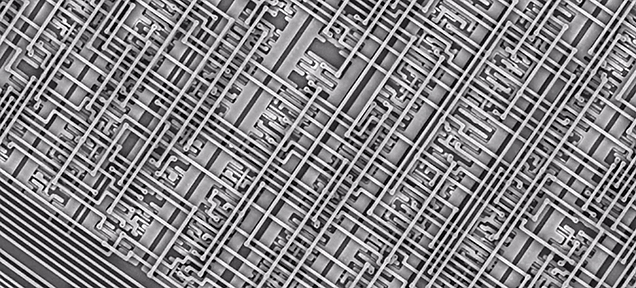
Transistors on modern microcircuits. (Photo taken by electron microscope.)
According to Shalaker, one of the main obstacles to computer processing speed is memory.
Processing large amounts of data requires a request for previously unknown data that has not yet been cached. In such cases, it will take a lot of time to complete a new request. A request for information to process a particular command will first go to the internal cache of the processor itself. Further, having searched all levels of the cache, the answer will be that there are no hits and the kernel will send a request to RAM. After searching the RAM, again, the answer will be that nothing was found. And only then the request will be sent to the HDD or SSD drive. The signal will have to go through relatively thick (for electrons) wires, overcoming the constant resistance. You must admit that this path is too long and during this period of time the kernel would have managed to finish processing several times already.
If you performed this request instead of your PC, then 96% of the time would have been waiting. It is also worth remembering that even when the CPU is waiting for the instruction to arrive, it still consumes electricity. An alternative solution is to combine the CPU and memory on the same plate. It just doesn’t work to place these two components on the same plate - a silicon wafer requires heating at 1000 ° C, which will lead to the melting of metal elements of a solid-state drive or hard drive.
To get around the temperature difference problem, the Stanford University team turned their attention to the one-dimensional carbon material discovered about 10 years ago - carbon nanotubes. These are extended cylindrical, mesh structures of carbon atoms with a diameter of one to several tens of nanometers. Low-temperature processing capabilities have become key in choosing a material for the silicon alternative. The processing temperature is only 200 of S.
CNT (carbon nanotube) have the properties of electrical conductivity, the silicon transistors are equal but their electrical properties depend on the angle of twist hexagonal graphite plane. Thus, scientists were able to achieve higher conductivity by 5 orders of magnitude.
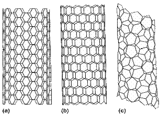
Three examples of nanotubes.
If we compare CNTs with silicon transistors under equal conditions and with the same architecture and device concept, then nanotubes will be much faster in performance, while consuming less energy.
Nevertheless, nanotubes grow randomly and are more like spaghetti brewed in a cup. Naturally, this option is not suitable for the production of microcircuits. Researchers have developed a method for growing CNTs in narrow grooves, giving them targeted growth. But this did not solve all the problems. While 99.5% of the nanotubes grow orderly, 5% stubbornly refuse to grow along the planned route. The way out of this situation was slightly unexpected. The holes in the region of defective CNTs allow the chip to work exactly as expected, neutralizing the growth defects of nanotubes.
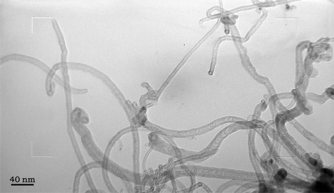
Nanotube growth. (Photo taken by electron microscope.)
Another emerging problem prophesied to ruin the whole undertaking. Although the semiconductivity of most grown tubes is silicon, the rest has the conductivity of ordinary metal. Unfortunately, scientists were at a loss to predict which of the tubes would be defective. These few CNTs could destroy the entire chip. But here a solution was found - Shalaker and his colleagues simply applied huge voltage pulses to the chip. Thus, the conductors acted as fuses and burned out under the action of high voltage. And only semiconductors remained on the chip.
This team had already created a computer based on CNTs, but it was slow and cumbersome with a relatively small number of transistors. The processor of this device is comparable in power to the Intel 4004, released in 1971. The first nanotube-based processor contained 178 transistors; their approximate length ranged from 10 to 200 nanometers.
Max Shalaker, in his hands is a previously manufactured wafer with chips based on silicon nanotubes.
Now, researchers led by Shalaker have created a system for stacking memory together with transistor layers, connecting them with tiny layers. The new structure significantly saves the time of requests and, accordingly, the time of complete processing of the team. 1000 times faster than similar systems of equal performance. Using the new architecture, the team has created many sensor plates that detect everything from infrared light to certain chemicals in the environment.
Earlier, I wrote an article about an alternative to silicon in the form of semiconductors based on InGaAs . Here is another one in the form of carbon nanotubes.
And what alternatives to silicon, like a semiconductor, do you know? Which ones are suitable for microchips of the future?
According to Max Shulaker, a member of the chip design team and a Ph.D. candidate in electrical engineering at Stanford University of California, such a 3D project significantly saves space in the system and increases the speed of data processing. This is achieved due to the fact that scientists contain a memory that stores all the data and compact the number of processors in a miniature space.
Reducing the distance between two elements can significantly speed up the processing time of commands by a computer.
Photo by Max Schalaker.
Slowdown
Computational capabilities of computer systems over the past 50 years have been constantly improved. This is largely due to the ability to continuously reduce silicon transistors and three-way switches with which logical operations are performed.
According to Moore's Law, a gross rule formulated by Gordon E. Moore in 1965, the number of silicon transistors on a chip must double every two years. Which is true, to further follow the rule, you need to reduce tiny silicon transistors to 5 nanometers. But here a problem arises - the limit for silicon, which is 7 nanometers (for comparison, the size of a human hair is on average about 100,000 nanometers). Subsequent downscaling will lead to the fact that the quantum effect of particles can disrupt its functioning. Accordingly, the law of moore will come to its logical end in the next ten years. In addition, an endless increase in the number of transistors on a chip is not the only method of increasing system performance.
Transistors on modern microcircuits. (Photo taken by electron microscope.)
Communication problem
According to Shalaker, one of the main obstacles to computer processing speed is memory.
Processing large amounts of data requires a request for previously unknown data that has not yet been cached. In such cases, it will take a lot of time to complete a new request. A request for information to process a particular command will first go to the internal cache of the processor itself. Further, having searched all levels of the cache, the answer will be that there are no hits and the kernel will send a request to RAM. After searching the RAM, again, the answer will be that nothing was found. And only then the request will be sent to the HDD or SSD drive. The signal will have to go through relatively thick (for electrons) wires, overcoming the constant resistance. You must admit that this path is too long and during this period of time the kernel would have managed to finish processing several times already.
If you performed this request instead of your PC, then 96% of the time would have been waiting. It is also worth remembering that even when the CPU is waiting for the instruction to arrive, it still consumes electricity. An alternative solution is to combine the CPU and memory on the same plate. It just doesn’t work to place these two components on the same plate - a silicon wafer requires heating at 1000 ° C, which will lead to the melting of metal elements of a solid-state drive or hard drive.
Carbon nanotubes
To get around the temperature difference problem, the Stanford University team turned their attention to the one-dimensional carbon material discovered about 10 years ago - carbon nanotubes. These are extended cylindrical, mesh structures of carbon atoms with a diameter of one to several tens of nanometers. Low-temperature processing capabilities have become key in choosing a material for the silicon alternative. The processing temperature is only 200 of S.
CNT (carbon nanotube) have the properties of electrical conductivity, the silicon transistors are equal but their electrical properties depend on the angle of twist hexagonal graphite plane. Thus, scientists were able to achieve higher conductivity by 5 orders of magnitude.
Three examples of nanotubes.
If we compare CNTs with silicon transistors under equal conditions and with the same architecture and device concept, then nanotubes will be much faster in performance, while consuming less energy.
Nevertheless, nanotubes grow randomly and are more like spaghetti brewed in a cup. Naturally, this option is not suitable for the production of microcircuits. Researchers have developed a method for growing CNTs in narrow grooves, giving them targeted growth. But this did not solve all the problems. While 99.5% of the nanotubes grow orderly, 5% stubbornly refuse to grow along the planned route. The way out of this situation was slightly unexpected. The holes in the region of defective CNTs allow the chip to work exactly as expected, neutralizing the growth defects of nanotubes.
Nanotube growth. (Photo taken by electron microscope.)
Another emerging problem prophesied to ruin the whole undertaking. Although the semiconductivity of most grown tubes is silicon, the rest has the conductivity of ordinary metal. Unfortunately, scientists were at a loss to predict which of the tubes would be defective. These few CNTs could destroy the entire chip. But here a solution was found - Shalaker and his colleagues simply applied huge voltage pulses to the chip. Thus, the conductors acted as fuses and burned out under the action of high voltage. And only semiconductors remained on the chip.
This team had already created a computer based on CNTs, but it was slow and cumbersome with a relatively small number of transistors. The processor of this device is comparable in power to the Intel 4004, released in 1971. The first nanotube-based processor contained 178 transistors; their approximate length ranged from 10 to 200 nanometers.
Max Shalaker, in his hands is a previously manufactured wafer with chips based on silicon nanotubes.
Now, researchers led by Shalaker have created a system for stacking memory together with transistor layers, connecting them with tiny layers. The new structure significantly saves the time of requests and, accordingly, the time of complete processing of the team. 1000 times faster than similar systems of equal performance. Using the new architecture, the team has created many sensor plates that detect everything from infrared light to certain chemicals in the environment.
Earlier, I wrote an article about an alternative to silicon in the form of semiconductors based on InGaAs . Here is another one in the form of carbon nanotubes.
And what alternatives to silicon, like a semiconductor, do you know? Which ones are suitable for microchips of the future?