October 12, 2017 at 18:16
AMD Ryzen: Inside Look
The characteristics of the AMD Ryzen processors and gaming stations based on them allow us to cautiously assume the end of a difficult period for the “alternative” chip maker and claim to be the leader. Without pretending to be the ultimate truth, we will analyze some details - functional extensions of the basic set of x86 instructions in the AMD Family 17h processor family.

List of technologies and instructions supported by AMD CPU 17h family. Excerpt from Software Optimization Guide for AMD Family 17h Processors.
The most complex devices, which are modern CPUs, can be considered from different points of view, coming to diametrically opposite conclusions and comparison results. However, most of the technologies discussed below were previously implemented in Intel processors, with the exception of the CLZERO instruction exclusive to AMD .

The SMAP option affects the page translation engine and the virtual memory subsystem. Allows you to block access of the privileged code of the operating system (Kernel Mode) to the pages of the user level (User Mode).
Such a restriction, which is somewhat contrary to the classical hierarchy of memory protection (in which the status of the supervisor allows for any kind of access), in some cases helps to counter the actions of malicious code that unauthorized uses supervisor mode, as well as to simplify the detection of some errors that lead to distortion of the contents of the memory.

The RDSEED statement, like the pre-existing RDRAND instruction, generates a random number. The difference is that RDSEED for each generated number uses an analog source of entropy (Enhanced non-deterministic random bit generator, NRBG). RDRAND uses a digital generator (Deterministic random bit generator, DRBG), periodically reloaded from an analog source of entropy. This reboot is called re-seed. The disadvantage of the RDRAND instruction is that in the pauses between such reboots several random numbers can be generated, and in this case the generation of each next number in this group of numbers is the result of the operation of a digital automaton (DRBG), rather than an analog source of entropy (NRBG), which theoretically reduces cryptographic strength.
This official interpretation of the differences between RDRAND and RDSEED is provided in the Intel documentation. Perhaps there are some Implementation-Specific differences between Intel and AMD. Simply put, you can give this recommendation: if the priority is the performance of the random number generator, you should use the RDRAND instruction, if the cryptographic strength is RDSEED.
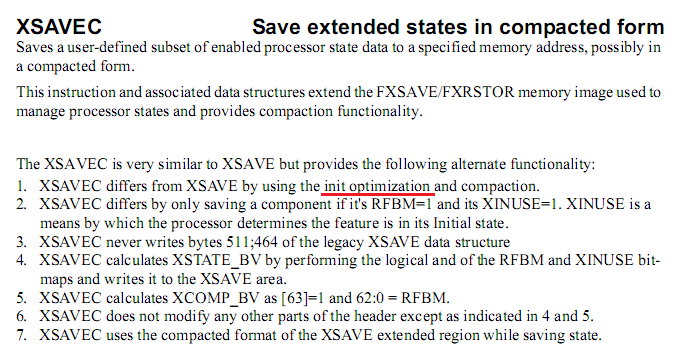
The XSAVEC instruction is one of the optimized forms of the XSAVE context preservation instruction used to support multi-tasking operating systems. The XSAVEC instruction, unlike XSAVE, does not save processor context components whose state has not changed since init optimization.
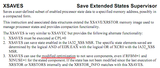
The XSAVES instruction is one of the optimized forms of the XSAVE context preservation instruction used to support multi-tasking operating systems. An XSAVES instruction, unlike XSAVE, does not save processor context components whose state has not changed since the previous restoration of their state (modified optimization). This form of optimization is typical for privileged operating system procedures.

The CLFLUSHOPT statement declares an invalid cache line. If, before executing the instruction, the line contained data waiting for a deferred write to RAM, such a write is performed before clearing the line. CLFLUSHOPT is an optimized version of a pre-existing CLFLUSH instruction. Unfortunately, a clear formalization of the list of differences between CLFLUSH and CLFLUSHOPT is missing in the Intel and AMD documentation.
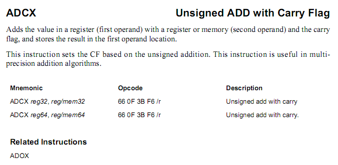
The ADCX and ADOX instructions perform unsigned addition of two operands and are intended for processing numbers whose bit capacity exceeds the bit capacity of one addition operation for several such operations. The sign of arithmetic transfer is taken into account during addition and is set in accordance with its results.
There are the following differences from the classic ADC instruction, which also performs addition using the carry flag:
The described atypical format for using flags allows optimizing the parallel execution of two multi-digit addition operations, alternating instructions related to two branches. When using the classic ADC instruction, such an alternation of instructions of mutually independent branches in one thread would be impossible, due to the use of a common carry flag (CF).
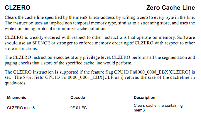
The CLZERO statement resets the contents of a given cache line. It can be used to quickly zero out cached memory areas as well as to eliminate additional transfers between cache memory and DRAM, which occur in cases where the contents of the cache line are partially modified. Thus, the interaction of Cache and DRAM is optimized.
To evaluate the effect of the CLZERO instruction exclusive to AMD, you will need to thoroughly recall the theory: the information that the processor processes can be classified as temporal and non-temporal.
By default, most processor instructions for accessing memory operate in temporal mode, for non-temporal access special instructions are used, for example movntps and / or movntpd .
With that said, the processor performs a write operation differently:
The CLZERO instruction, which atomically performs complete zeroing of the cache line, eliminates the need for additional loading of information from RAM when generating reliable contents of the line. In this way, it differs from typical write operations of lower capacity, which modify the cache line partially. In addition, an explicit data dimension of 64 bytes or 512 bits simplifies write-combining optimization.
Note .
For convenience of presentation, the cache line size is taken equal to 64 bytes. This is a typical value for modern Intel and AMD processors. In general, the programmer should detect the value of this parameter using the CPUID instruction, avoiding the use of predefined constants.
Analyzing the considered list of functional extensions, we can conclude that the developers focused on protecting user data, reducing the cost of processor cycles to switch context in a multitasking environment, optimizing the interaction of cache memory and RAM, as well as basic arithmetic operations with high-resolution integers.
The information was collected from various sources, the process of clarification and verification has not been completed at the moment, so comments and additions are welcome, especially regarding the CLFLUSHOPT and CLZERO instructions and the features of various processors not standardized by the official Implementation-Specific documentation.
List of technologies and instructions supported by AMD CPU 17h family. Excerpt from Software Optimization Guide for AMD Family 17h Processors.
The most complex devices, which are modern CPUs, can be considered from different points of view, coming to diametrically opposite conclusions and comparison results. However, most of the technologies discussed below were previously implemented in Intel processors, with the exception of the CLZERO instruction exclusive to AMD .
SMAP, Supervisor Mode Access Prevention
- Intel and AMD
The SMAP option affects the page translation engine and the virtual memory subsystem. Allows you to block access of the privileged code of the operating system (Kernel Mode) to the pages of the user level (User Mode).
Such a restriction, which is somewhat contrary to the classical hierarchy of memory protection (in which the status of the supervisor allows for any kind of access), in some cases helps to counter the actions of malicious code that unauthorized uses supervisor mode, as well as to simplify the detection of some errors that lead to distortion of the contents of the memory.
RDSEED, Read Random Number (Re-Seed)
- Intel and AMD
The RDSEED statement, like the pre-existing RDRAND instruction, generates a random number. The difference is that RDSEED for each generated number uses an analog source of entropy (Enhanced non-deterministic random bit generator, NRBG). RDRAND uses a digital generator (Deterministic random bit generator, DRBG), periodically reloaded from an analog source of entropy. This reboot is called re-seed. The disadvantage of the RDRAND instruction is that in the pauses between such reboots several random numbers can be generated, and in this case the generation of each next number in this group of numbers is the result of the operation of a digital automaton (DRBG), rather than an analog source of entropy (NRBG), which theoretically reduces cryptographic strength.
This official interpretation of the differences between RDRAND and RDSEED is provided in the Intel documentation. Perhaps there are some Implementation-Specific differences between Intel and AMD. Simply put, you can give this recommendation: if the priority is the performance of the random number generator, you should use the RDRAND instruction, if the cryptographic strength is RDSEED.
XSAVEC, Extended Save with Compaction
- Intel and AMD
The XSAVEC instruction is one of the optimized forms of the XSAVE context preservation instruction used to support multi-tasking operating systems. The XSAVEC instruction, unlike XSAVE, does not save processor context components whose state has not changed since init optimization.
XSAVES, Extended Save for Supervisor
- Intel and AMD
The XSAVES instruction is one of the optimized forms of the XSAVE context preservation instruction used to support multi-tasking operating systems. An XSAVES instruction, unlike XSAVE, does not save processor context components whose state has not changed since the previous restoration of their state (modified optimization). This form of optimization is typical for privileged operating system procedures.
CLFLUSHOPT, Cache Line Flush Optimized
- Intel and AMD
The CLFLUSHOPT statement declares an invalid cache line. If, before executing the instruction, the line contained data waiting for a deferred write to RAM, such a write is performed before clearing the line. CLFLUSHOPT is an optimized version of a pre-existing CLFLUSH instruction. Unfortunately, a clear formalization of the list of differences between CLFLUSH and CLFLUSHOPT is missing in the Intel and AMD documentation.
ADCX, Add with Carry Flag for Multi-Precision
- Intel and AMD
The ADCX and ADOX instructions perform unsigned addition of two operands and are intended for processing numbers whose bit capacity exceeds the bit capacity of one addition operation for several such operations. The sign of arithmetic transfer is taken into account during addition and is set in accordance with its results.
There are the following differences from the classic ADC instruction, which also performs addition using the carry flag:
- The ADCX instruction does not modify the OF overflow flag.
- The ADOX instruction uses the overflow flag (OF) as a sign of arithmetic transfer and does not modify the CF transfer flag.
The described atypical format for using flags allows optimizing the parallel execution of two multi-digit addition operations, alternating instructions related to two branches. When using the classic ADC instruction, such an alternation of instructions of mutually independent branches in one thread would be impossible, due to the use of a common carry flag (CF).
CLZERO, Cache Line Zero
- AMD only
The CLZERO statement resets the contents of a given cache line. It can be used to quickly zero out cached memory areas as well as to eliminate additional transfers between cache memory and DRAM, which occur in cases where the contents of the cache line are partially modified. Thus, the interaction of Cache and DRAM is optimized.
To evaluate the effect of the CLZERO instruction exclusive to AMD, you will need to thoroughly recall the theory: the information that the processor processes can be classified as temporal and non-temporal.
- The temporal type includes data that the processor intensively and repeatedly uses at the current time, while their total size is less than the size of the cache. Placing such data in the cache improves performance by eliminating the need for access to RAM.
- Non-temporal data are data types that are useless and often harmful to cache. If the size of the processed block exceeds the cache size, or the next access to the data is planned after a long time, such data is highly likely to be pushed out of the cache before the next access to it, which means that reading RAM will again be required. In such an example, caching unproductively consumes CPU cycles and cache size.
By default, most processor instructions for accessing memory operate in temporal mode, for non-temporal access special instructions are used, for example movntps and / or movntpd .
With that said, the processor performs a write operation differently:
- Writing in temporal store mode involves pre-filling the cache line; for this, the 64-byte RAM area that the target write operation affects is read and cached. Actually, the data update prescribed by the write instruction is already performed in the cache.
- Recording in the non-temporal store (streaming store) mode implies only writing to RAM, without preliminary “speculative” reading, although it allows combining a series of several write cycles of low bit capacity into a general write combining cycle.
The CLZERO instruction, which atomically performs complete zeroing of the cache line, eliminates the need for additional loading of information from RAM when generating reliable contents of the line. In this way, it differs from typical write operations of lower capacity, which modify the cache line partially. In addition, an explicit data dimension of 64 bytes or 512 bits simplifies write-combining optimization.
Note .
For convenience of presentation, the cache line size is taken equal to 64 bytes. This is a typical value for modern Intel and AMD processors. In general, the programmer should detect the value of this parameter using the CPUID instruction, avoiding the use of predefined constants.
Instead of an afterword
Analyzing the considered list of functional extensions, we can conclude that the developers focused on protecting user data, reducing the cost of processor cycles to switch context in a multitasking environment, optimizing the interaction of cache memory and RAM, as well as basic arithmetic operations with high-resolution integers.
The information was collected from various sources, the process of clarification and verification has not been completed at the moment, so comments and additions are welcome, especially regarding the CLFLUSHOPT and CLZERO instructions and the features of various processors not standardized by the official Implementation-Specific documentation.