May 23, 2018 at 10:14
The insides of the ADR chip AD9361 - when microelectronics is more profitable than drug trafficking
When Analog Devices released the AD9361 SDR transceiver in 2013, there was a real revolution in digital radio communications. There were SDRs before, but now it was possible to get everything in one chip: 2 channels for reception and 2 for transmission (with on-board 12-bit DAC and ADC) with a channel width of up to 56 MHz, local generators and radio path - for operation in the range from 70 (for transmission from 47) to 6000 MHz. On the AD9361 «out of the box" can implement almost any digital transceiver, except perhaps only 500MHz, lower noise level">UWB and is beginning to gain popularity 60GHz band (but there is no hardware multi-element phased array everything is almost nothing to do anyway). It remains only to add the source / receiver of data (for now this is usually FPGA), external filters and LNA / PAif the task requires it.
I finally managed to see what was inside it, and to try to look at the financial side of the production of truly innovative microelectronics with high added value.
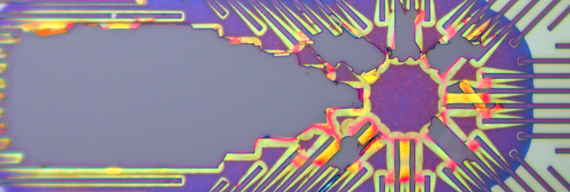
After opening - we see a chip measuring 4336x4730 µm, looking ahead - production standards are 65nm. Only coils from PLL (right top and left in the middle) catch the eye and - the fact that the masks were released in 2011, and the chip went on sale - only at the end of 2013. By click - full resolution (72MB): After etching almost everyone layers of metal compounds - it is clear that the vast majority of the microcircuit is occupied by analog blocks:

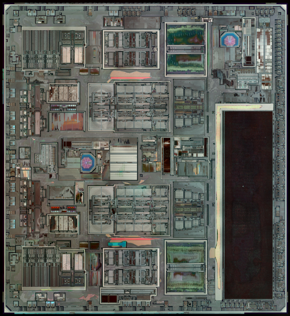
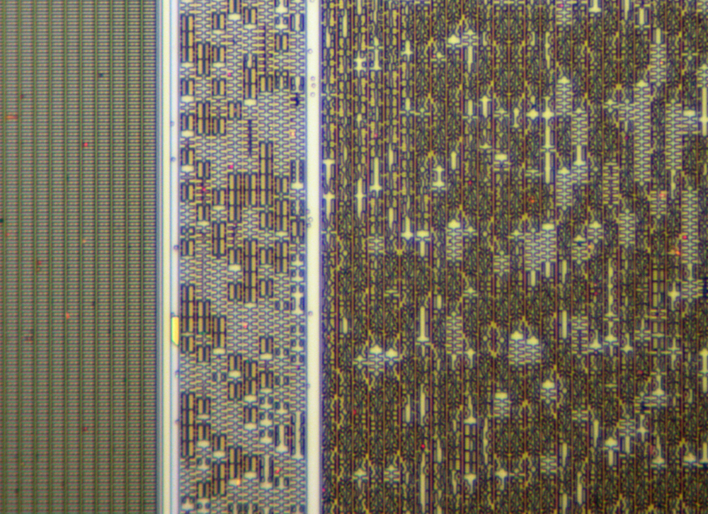
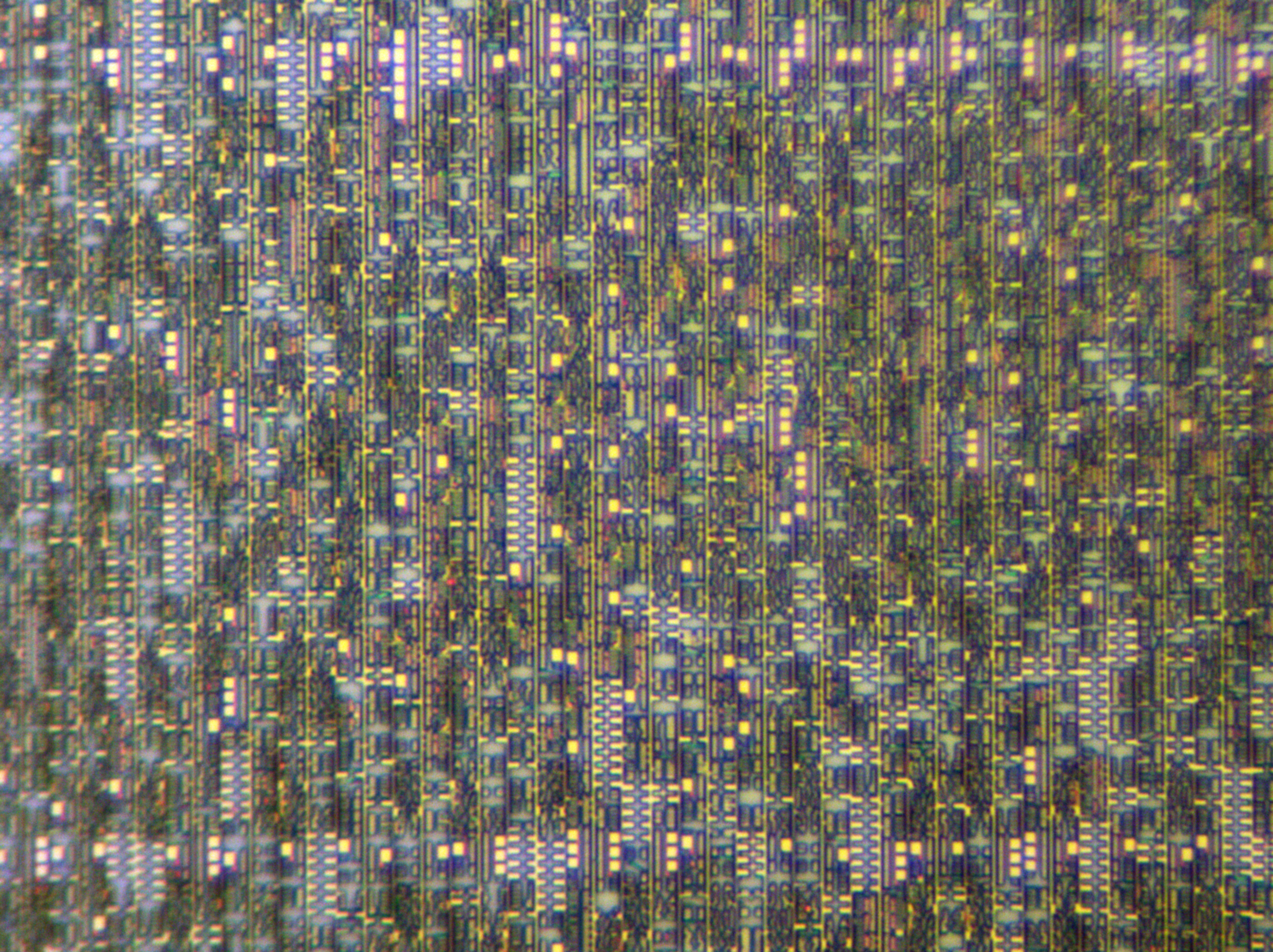
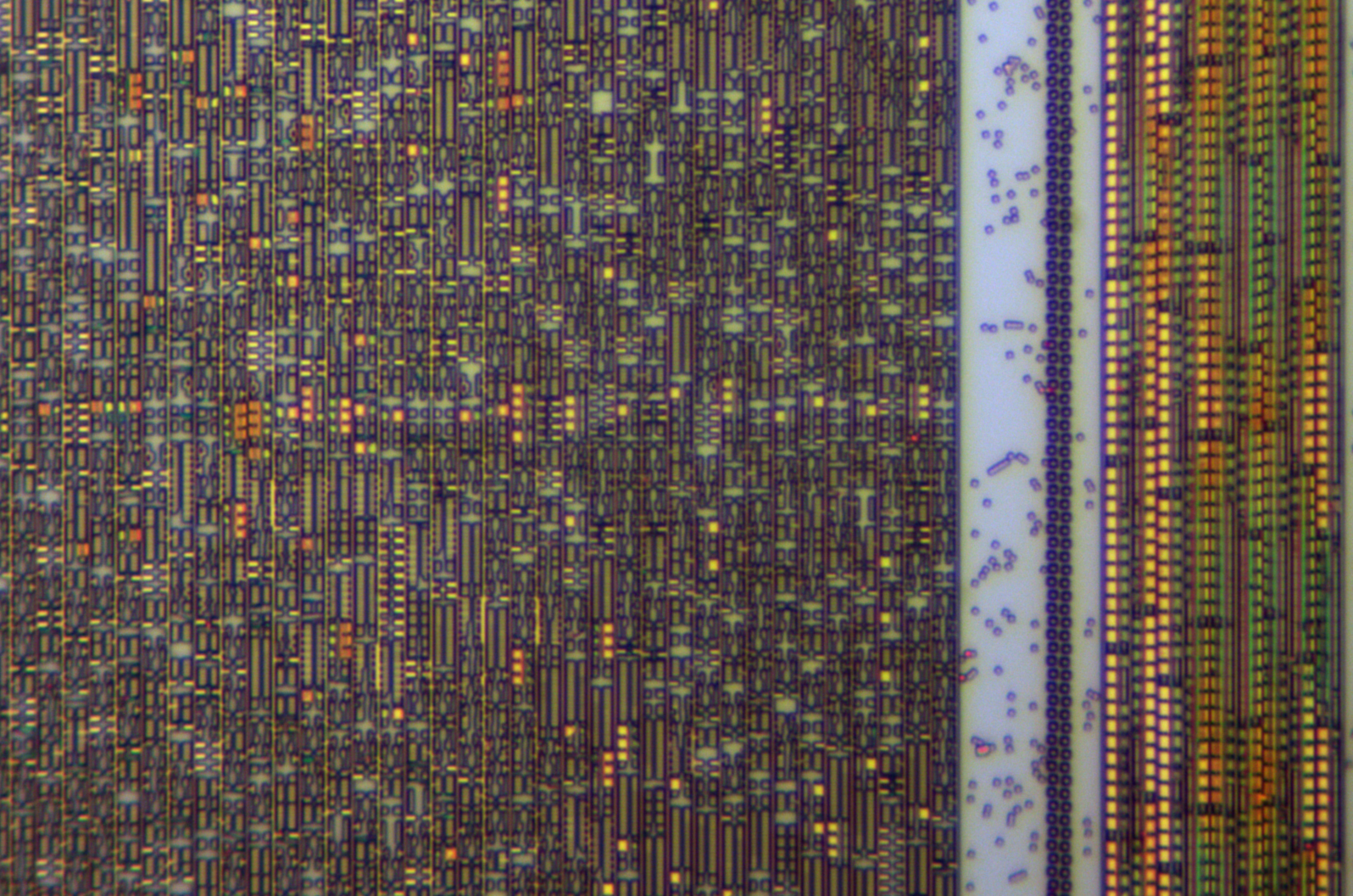
At the bottom right is the digital stuffing. At maximum magnification, we see rows of standard cells. The cells are, like almost everyone, “back to back”, [PFET NFET] [NFET PFET] and thus use the common vertical lines VCC and GND (of course, power is supplied from the upper levels of the metal, which are no longer visible here). PFET transistors are a bit wider (as always in silicon CMOS processes). The cell width is 1.83 μm, which is approximately similar to the truth for a 65 nm chip. The scale after clicking on full resolution in this photo and beyond is 24.5nm per pixel.
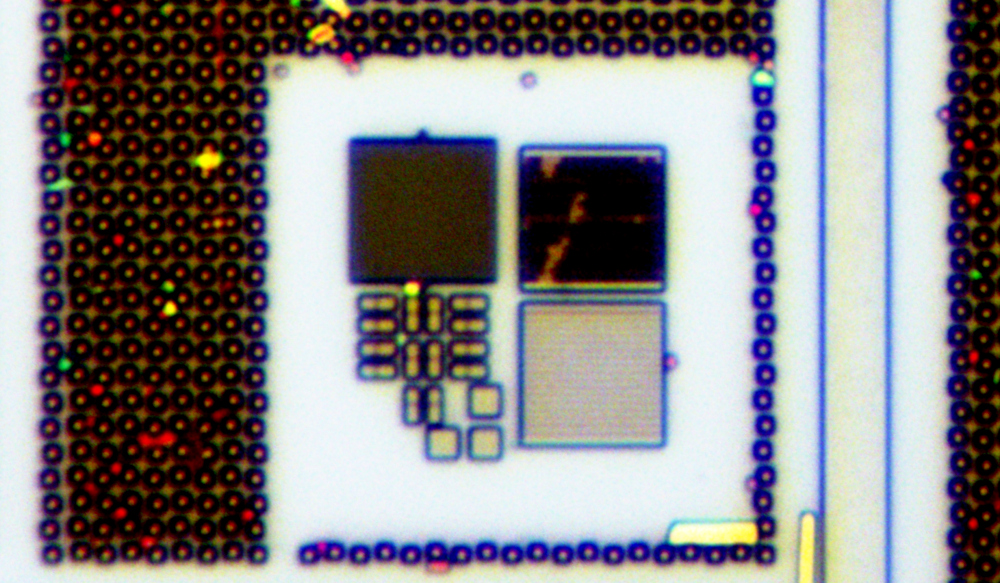
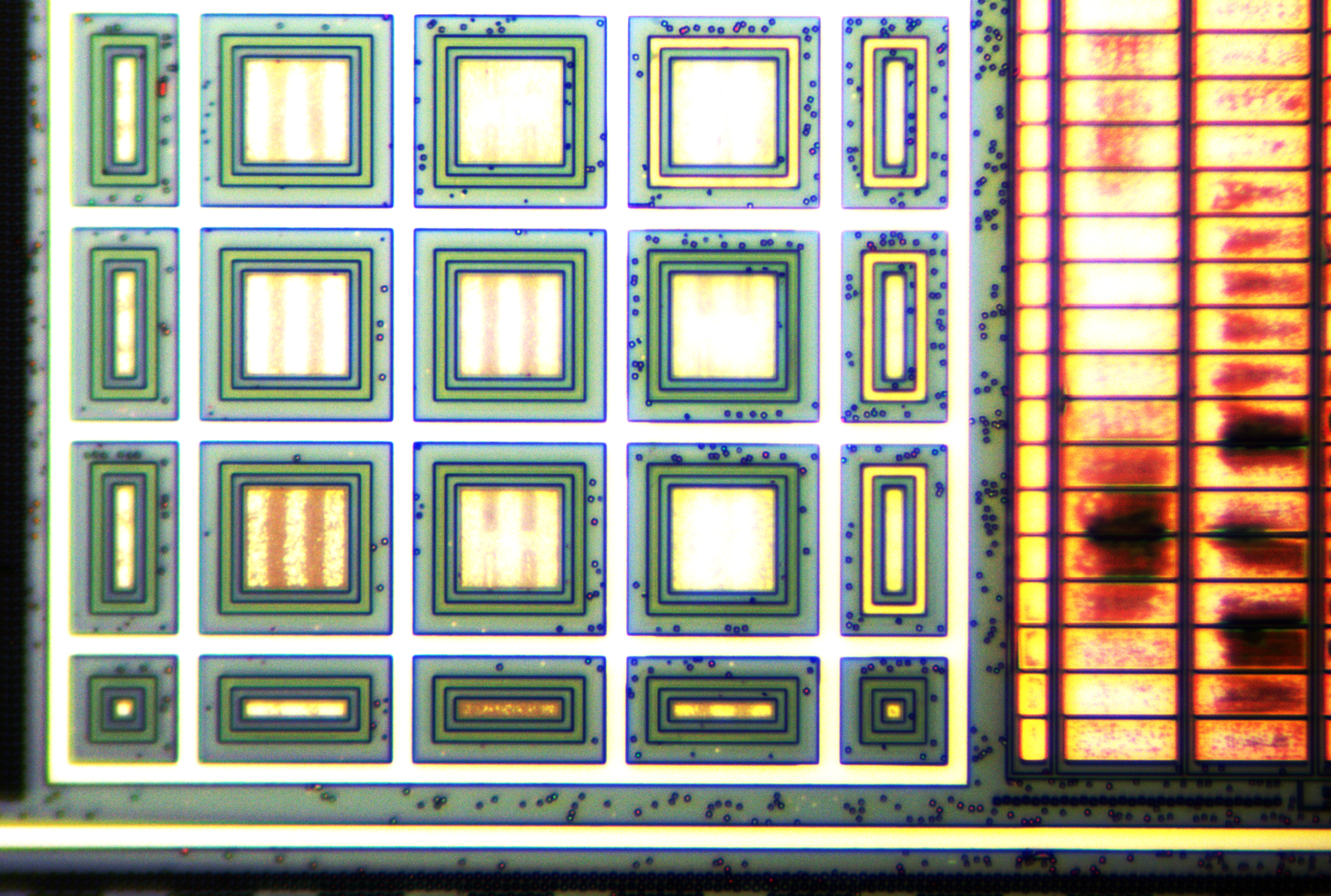
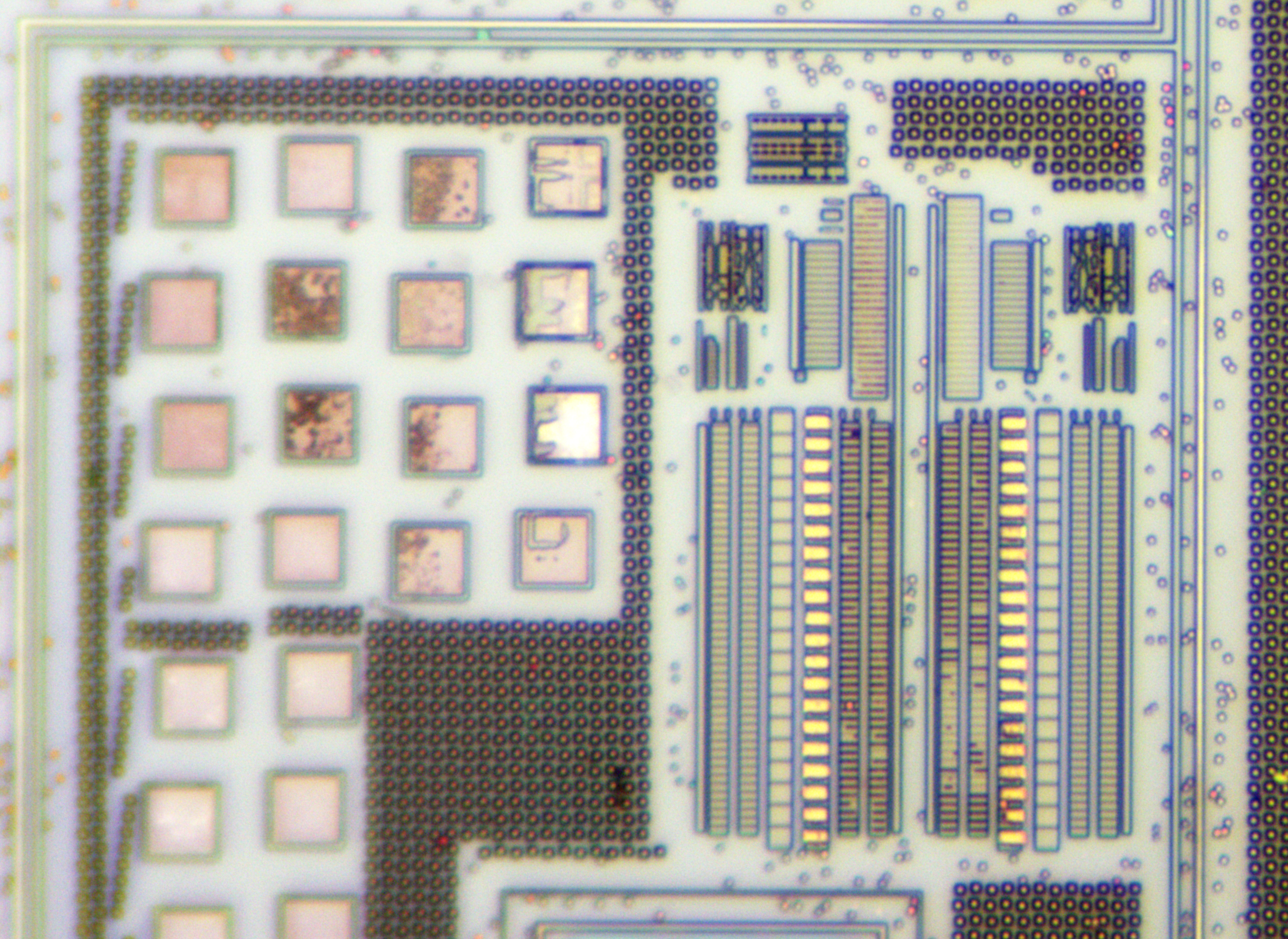
Blocks are scattered throughout the crystal area, which are probably used to check the spread of transistor characteristics over the crystal area, at the initial stage of sorting or even testing the process. However, there is no access to them after the completion of production of all metallization levels of the final chip - there is nowhere to connect to the upper metals, and the complex digital circuitry for JTAG is also not visible nearby: Capacitor arrays are a key element of the DAC / ADC implementation, the identity of the capacitors in the array is crucial, here along the edges - it looks like additional dummy elements so that the edge effects of photolithography do not affect the size / capacity.

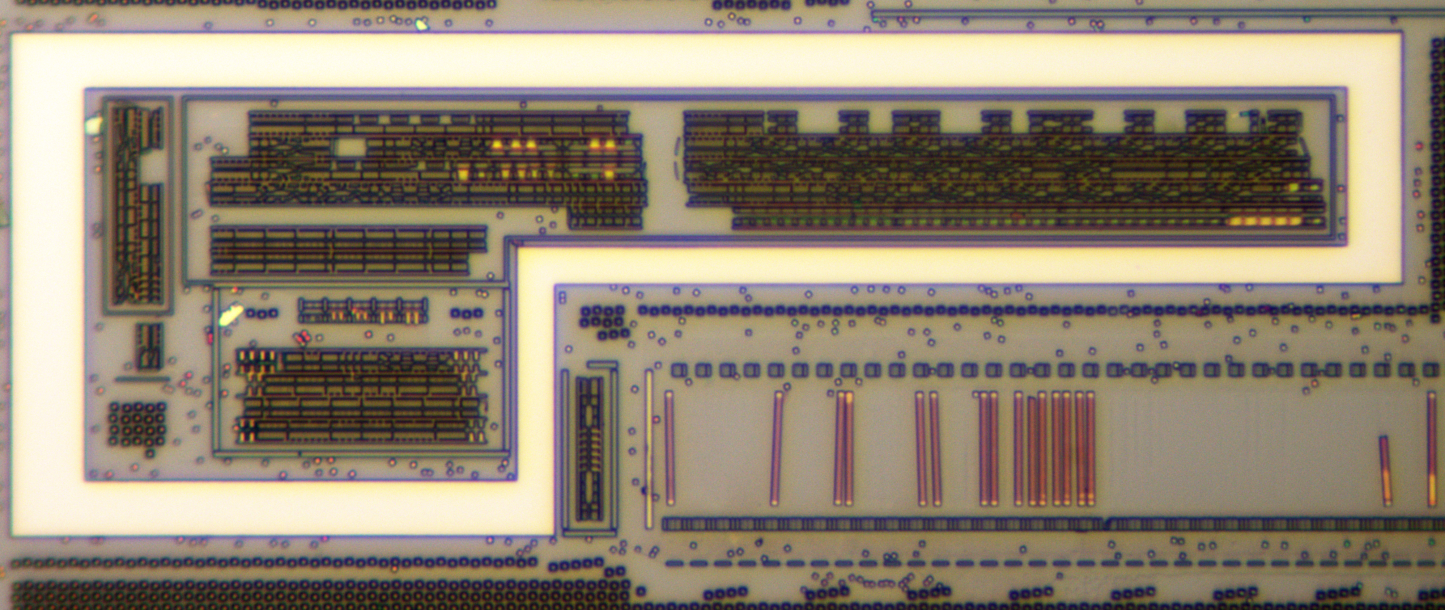
I did not find a single SRAM array on the chip. The only regular digital structure is on this frame on the left, but in terms of topology it does not look like SRAM. It doesn't look like anything at all. There is no way to figure it out without an electron microscope. All analog stuffing - mainly on field-effect transistors:

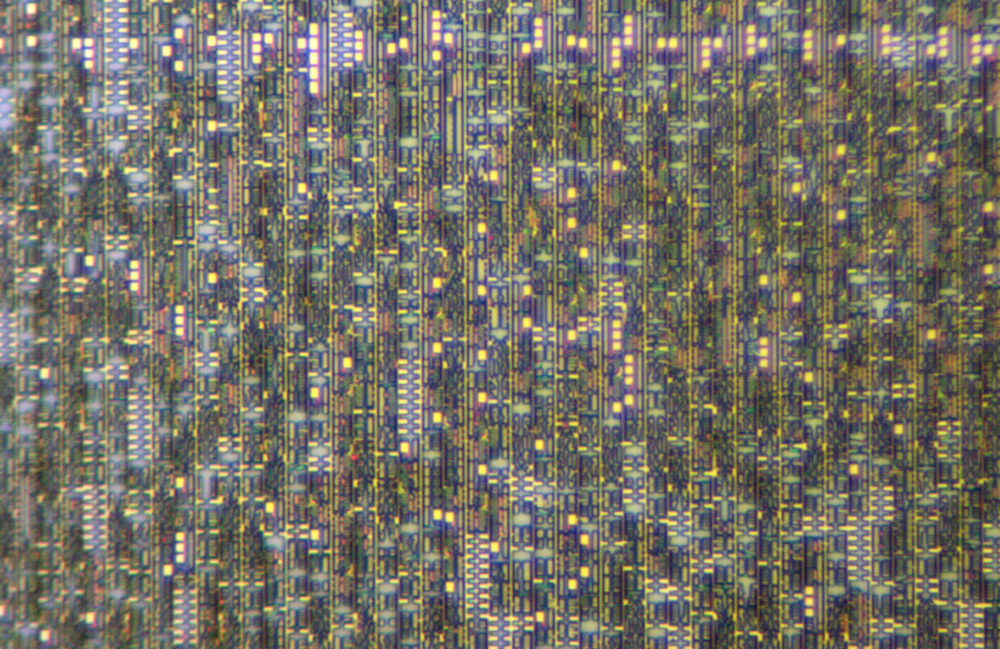
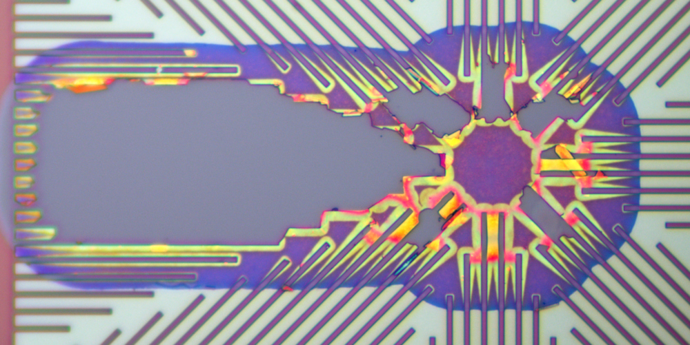
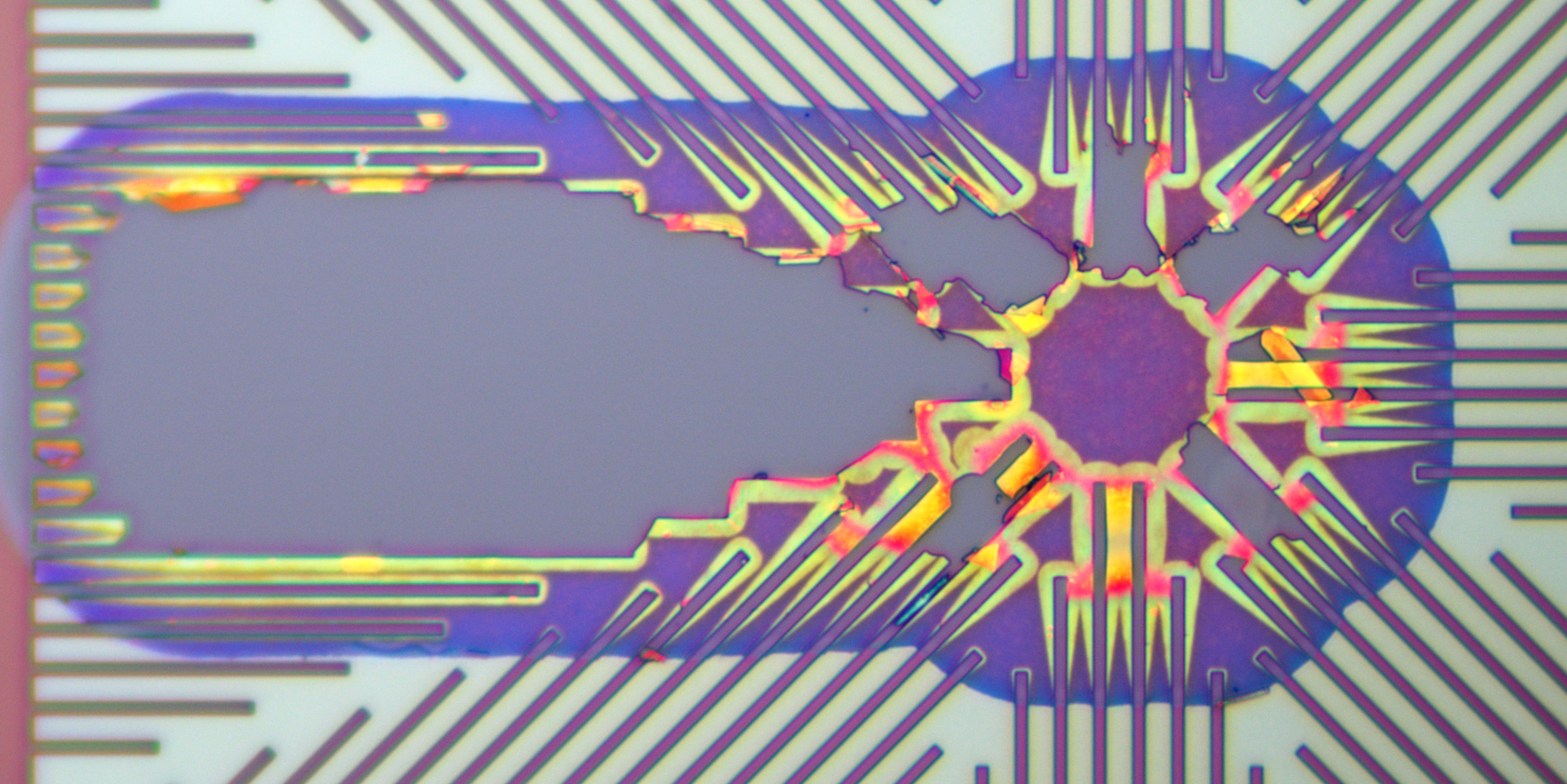
Well, the title photo is all that remains of the PLL inductance (with not completely etched metal and glass - which gives such colors). PLL here is the most crucial part. If noise or insufficient linearity of the analog path can still be circumvented by an external body kit and digital processing, then the phase noise PLL - set an absolute and insurmountable limit on the quality of radio communication:
Using the example of this chip, you can roughly calculate how the financial side of a really high-tech product looks like from a bird's eye view and, to a first approximation, fortunately, the annual financial statements of Analog Devices are public, and we can now evaluate the cost. There is always room for fault with the accuracy of such rough estimates, but here the main principle is the main principle (you can go into details endlessly, starting with packaging and testing ...):
The area of the microcircuit is ~ 21.12 mm², the useful area of a silicon wafer with a diameter of 300 mm (and at 65 nm only such) - approximately 65'000 mm². Thus, from one plate we get 3077 microcircuits, with a suitable 50% yield, 1538 pieces remain. At a plate price of $ 1,600 (the technology is already old) - the cost of each suitable crystal is $ 1.04.
NRE (Non recurring engineering) - masks (2 sets for $ 400 thousand) and equipment - for example, $ 1 million in total. If you estimate the total volume of production at 1000 plates (but in reality there may be more) - NRE for each chip will add $ 0.64.
The retail price for AD9361 from distributors is $ 275, wholesale from the manufacturer is $ 175.
At Analog Devices at $ 1.68 cost - it turns out $ 173.32 value added! Even vertically integrated drug cartels cannot boast of such rates! Intel, for example, also cannot boast of such added value - the cost there is 1.5 orders of magnitude higher.
But here, of course, there is an obvious problem - you can’t just take and make an integrated SDR transceiver: you need patents that allow you to work for years (generalized - intellectual property) - and the chip itself needs to be developed. Therefore, we direct part of the proceeds to further research and development in order to release new, more advanced products in the future.
From the 2017 Analog Devices report, we see that with revenue of $ 5.1 billion, R&D expenses amounted to $ 968 million, and profit before taxes was $ 3.061 billion. In this proportion, the revenue is divided. Of course, in different products everything is different, but on average it will turn out something like this:

Thus, it is not enough to build a conditional 14nm plant for $ 10 billion. You need to spend ~ 15 times more on product development for him. And then - the same amount for promotion and support, so that the product is sold worldwide. And that means there is still a lot of work ahead.
You can see more photos of microchips at zeptobars.com ( RSS ). And if you want more open chips, you can even support the Patreon project .
I finally managed to see what was inside it, and to try to look at the financial side of the production of truly innovative microelectronics with high added value.
Time to get acid
After opening - we see a chip measuring 4336x4730 µm, looking ahead - production standards are 65nm. Only coils from PLL (right top and left in the middle) catch the eye and - the fact that the masks were released in 2011, and the chip went on sale - only at the end of 2013. By click - full resolution (72MB): After etching almost everyone layers of metal compounds - it is clear that the vast majority of the microcircuit is occupied by analog blocks:
At the bottom right is the digital stuffing. At maximum magnification, we see rows of standard cells. The cells are, like almost everyone, “back to back”, [PFET NFET] [NFET PFET] and thus use the common vertical lines VCC and GND (of course, power is supplied from the upper levels of the metal, which are no longer visible here). PFET transistors are a bit wider (as always in silicon CMOS processes). The cell width is 1.83 μm, which is approximately similar to the truth for a 65 nm chip. The scale after clicking on full resolution in this photo and beyond is 24.5nm per pixel.
Blocks are scattered throughout the crystal area, which are probably used to check the spread of transistor characteristics over the crystal area, at the initial stage of sorting or even testing the process. However, there is no access to them after the completion of production of all metallization levels of the final chip - there is nowhere to connect to the upper metals, and the complex digital circuitry for JTAG is also not visible nearby: Capacitor arrays are a key element of the DAC / ADC implementation, the identity of the capacitors in the array is crucial, here along the edges - it looks like additional dummy elements so that the edge effects of photolithography do not affect the size / capacity.

I did not find a single SRAM array on the chip. The only regular digital structure is on this frame on the left, but in terms of topology it does not look like SRAM. It doesn't look like anything at all. There is no way to figure it out without an electron microscope. All analog stuffing - mainly on field-effect transistors:
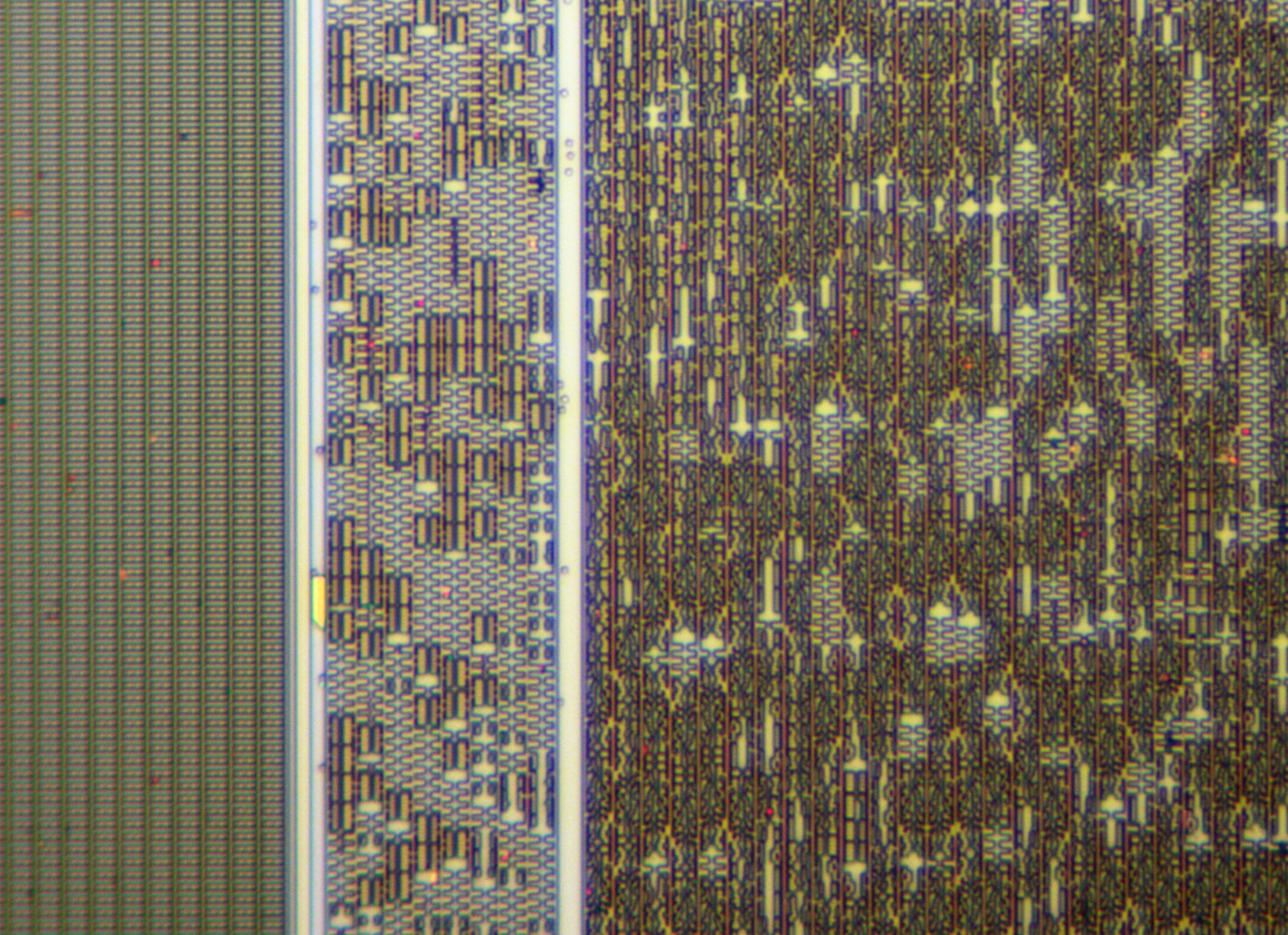
Some more digital stuffing


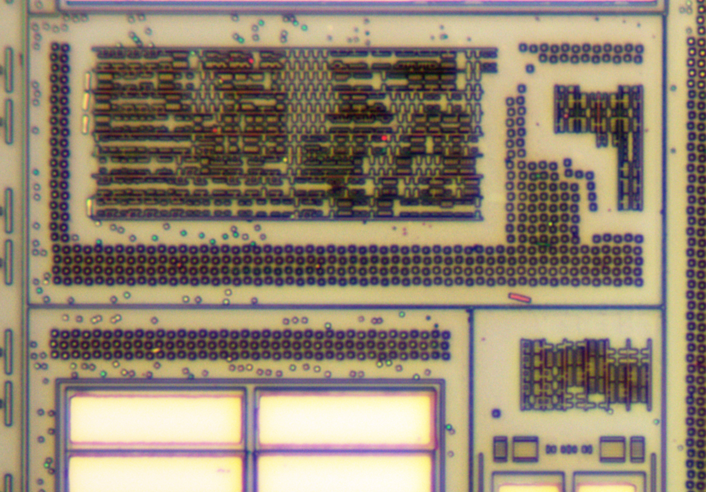
Well, the title photo is all that remains of the PLL inductance (with not completely etched metal and glass - which gives such colors). PLL here is the most crucial part. If noise or insufficient linearity of the analog path can still be circumvented by an external body kit and digital processing, then the phase noise PLL - set an absolute and insurmountable limit on the quality of radio communication:
And now for the calculator
Using the example of this chip, you can roughly calculate how the financial side of a really high-tech product looks like from a bird's eye view and, to a first approximation, fortunately, the annual financial statements of Analog Devices are public, and we can now evaluate the cost. There is always room for fault with the accuracy of such rough estimates, but here the main principle is the main principle (you can go into details endlessly, starting with packaging and testing ...):
The area of the microcircuit is ~ 21.12 mm², the useful area of a silicon wafer with a diameter of 300 mm (and at 65 nm only such) - approximately 65'000 mm². Thus, from one plate we get 3077 microcircuits, with a suitable 50% yield, 1538 pieces remain. At a plate price of $ 1,600 (the technology is already old) - the cost of each suitable crystal is $ 1.04.
NRE (Non recurring engineering) - masks (2 sets for $ 400 thousand) and equipment - for example, $ 1 million in total. If you estimate the total volume of production at 1000 plates (but in reality there may be more) - NRE for each chip will add $ 0.64.
The retail price for AD9361 from distributors is $ 275, wholesale from the manufacturer is $ 175.
At Analog Devices at $ 1.68 cost - it turns out $ 173.32 value added! Even vertically integrated drug cartels cannot boast of such rates! Intel, for example, also cannot boast of such added value - the cost there is 1.5 orders of magnitude higher.
But here, of course, there is an obvious problem - you can’t just take and make an integrated SDR transceiver: you need patents that allow you to work for years (generalized - intellectual property) - and the chip itself needs to be developed. Therefore, we direct part of the proceeds to further research and development in order to release new, more advanced products in the future.
From the 2017 Analog Devices report, we see that with revenue of $ 5.1 billion, R&D expenses amounted to $ 968 million, and profit before taxes was $ 3.061 billion. In this proportion, the revenue is divided. Of course, in different products everything is different, but on average it will turn out something like this:
Conclusions:
- All this talk about whether there are 65/28 / 14nm microelectronic factories in Russia or not is a piece of cake that is hardly visible on the diagram for this particular product. Development - requires 1.5 orders of magnitude more resources than directly mass production. Therefore, talking about production without investing 1.5 orders of magnitude more in development is simply self-deception. Most of the money is not made in production.
- This thin production piece of cake is not even production profit, but revenue. There is the same internal division: according to old technologies, on market conditions - 90% of the cost (mainly import) and loan servicing, 10% profit. Those. directly microelectronic plant here is good if you get $ 0.25 profit on the production of this chip. Only on the latest technologies (available to units in the world), where competition is limited, can profits be significantly higher.
- Any high-tech product - requires the maximum increase in sales (in pieces). Do not brush aside from the obvious thing. This means that it is impossible to sell only to one country - products must go to the whole world, otherwise it will not be competitive. With such a low cost of production - the relationship between the final price of the product and sales is linear. If we sell only to Russia (which, say, in electronics is 2% of the world), then we are forced to sell 50 times more in a first approximation.
- Sales are provided not only at a low price (which is achieved by spreading the development cost over a large volume), but also with “other expenses”, which are comparable to the development itself, which includes all these incomprehensible to the Russian soul free samples for poor students (who will not buy anything right now) , conferences, exhibitions and contests, advertising, and much more.
- If there is no unique IP / development, or all of this is purchased / licensed ready-made (as Rusnano tries to do according to the concept of pure capitalism), then you will have to be content with tiny fractions of the pie and modest profit margins (or self-deception). "Routine" microelectronic products, for example, are sold at the price of "only" 5-10x cost.
Thus, it is not enough to build a conditional 14nm plant for $ 10 billion. You need to spend ~ 15 times more on product development for him. And then - the same amount for promotion and support, so that the product is sold worldwide. And that means there is still a lot of work ahead.
You can see more photos of microchips at zeptobars.com ( RSS ). And if you want more open chips, you can even support the Patreon project .