Launch AMP applications on Cyclone V SoC
- Tutorial
If you read my previous article , you are probably interested in this topic and want to know more. In this article, we will consider a very private, not simple, but no less necessary task of launching two different Baremetal applications on different SoC Cyclone V cores. In essence, such systems are called AMP - asyncronus multi-processing. I almost forgot to say that in Russian you will not find another more correct and detailed guide to the creation of such systems, so read it!
Introduction
It is understood that the reader is already familiar with the standard libraries Altera HW Manager and SoCAL. But still, let's say a few words about them. SoC Abstraction Layer (SoCAL) contains low-level functions for convenient setting / reading of bits, bytes, words for direct control of HPS registers. Hardware Manager (HW Manager) is a set of more complex functions for writing baremetal applications, drivers, BPS and more. Be sure to read the documentation at this address / ip / altera / hps / altera_hps / doc / or in .h files.
Download program
First you need to remember how the program downloads, in my first article not much was said about this.
The HPS boot process has several stages, let's try to understand them ...
Immediately after switching on, the code located directly on the Cortex-A9 Flash memory called BootRom is executed. You cannot change it or even see its contents. It serves for primary initialization and in the next step transfers the boot process to SSBL (Second Stage Boot Loader, shortly called Preloader). What you need to know to understand the process is that the BootRom code, first of all, selects the Preloader download source, focus on the external physical pins of BSEL ...
And so, after the BootRom code is executed, the Preloader, necessary for setting Clock, SDRAM and so on, starts to load. After the program starts to run ...
Let's take a closer look at what happens after loading Preloader. Actually, after this the program starts to run, but not immediately from the main function main (). Before it, the _main () function is executed, the main task of which is mapping the application to the addresses in memory specified in the scatter file. This means that the entry point for the application is not at the beginning of the main () function code that we write, but in the special, invisible when writing code, _main () utility function that appears before main () during compilation. Perhaps everyone already knows this, but at that time it was a revelation to me, I thought that the entry point was at the beginning of main ().
Cores
All described processes are always executed on the first cpu0 core, the second core is always in a reset state. To start the second core, you must reset the corresponding bit of the MPUMODRST register in the RSTMGR group. Well, set the start address of the PC in the CPU1STARTADDR register in the SYSMGR group. However, after turning on the PC, cpu1 is 0x0. After running Preloader at 0x0, there is nothing useful, so before running cpu1, you must place the BootROM code at 0x0. I spent a lot of time to find out that it is only from the BootROM code that the CPU1STARTADDR register is read, after which the PC is set to the desired value. As it turned out, placing this code is not as trivial as it seems at first glance. To do this, we need the alt_addr_space_remap function from the HW manager, from the alt_address_space.h file.
alt_addr_space_remap(ALT_ADDR_SPACE_MPU_ZERO_AT_BOOTROM, ALT_ADDR_SPACE_NONMPU_ZERO_AT_SDRAM, ALT_ADDR_SPACE_H2F_ACCESSIBLE, ALT_ADDR_SPACE_LWH2F_ACCESSIBLE);Do not rush to rejoice, this is not enough for BootROM to be at 0x0. You must configure the L2 cache address filter. The description of the alt_addr_space_remap function says if you need to place the BootROM at 0x0, then configure this filter as follows, placing the code after the function.
uint32_t addr_filt_start;
uint32_t addr_filt_end;
alt_l2_addr_filter_cfg_get(&addr_filt_start, &addr_filt_end);
if (addr_filt_start != L2_CACHE_ADDR_FILTERING_START_RESET)
{
        alt_l2_addr_filter_cfg_set(L2_CACHE_ADDR_FILTERING_START_RESET, addr_filt_end);
}
Only after that we set the start address and can start the kernel.
alt_write_word(ALT_SYSMGR_ROMCODE_CPU1STARTADDR_ADDR, ALT_SYSMGR_ROMCODE_CPU1STARTADDR_VALUE_SET(0x100000)); //set PC of cpu1 to 0x00100000
alt_write_word(ALT_RSTMGR_MPUMODRST_ADDR, alt_read_byte(ALT_RSTMGR_MPUMODRST_ADDR) & ALT_RSTMGR_MPUMODRST_CPU1_CLR_MSK);
So what's next? And then you need a little understanding of the structure of the project.
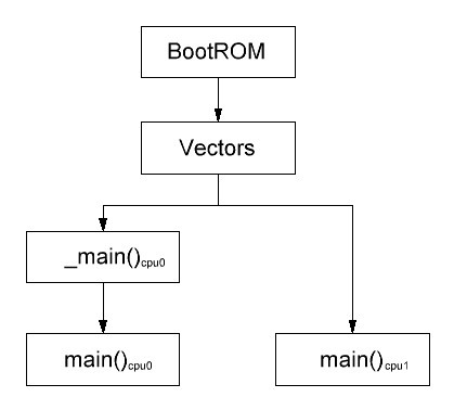
It is this structure for AMP projects that is the most optimal. The Vectors block defines interrupt vectors and branches for different processors. Interrupt vectors are common to each processor. Unfortunately, this block can only be written in assembler, but fortunately we won’t write it from scratch, we just edit the HW lib alt_interrupt_armcc.s library file. It announces the necessary interrupt vector, interrupt stack, support for FPU VFP \ NEON. Let's add the necessary splitter.
alt_interrupt_armcc.s before editing
    PRESERVE8
    AREA    VECTORS, CODE, READONLY
    ENTRY
    EXPORT alt_interrupt_vector
    IMPORT __main
    EXPORT alt_int_handler_irq [WEAK]
alt_interrupt_vector
Vectors
    LDR PC, alt_reset_addr
    LDR PC, alt_undef_addr
    LDR PC, alt_svc_addr
    LDR PC, alt_prefetch_addr
    LDR PC, alt_abort_addr
    LDR PC, alt_reserved_addr
    LDR PC, alt_irq_addr
    LDR PC, alt_fiq_addr
alt_reset_addr    DCD alt_int_handler_reset
alt_undef_addr    DCD alt_int_handler_undef
alt_svc_addr      DCD alt_int_handler_svc
alt_prefetch_addr DCD alt_int_handler_prefetch
alt_abort_addr    DCD alt_int_handler_abort
alt_reserved_addr DCD alt_int_handler_reserve
alt_irq_addr      DCD alt_int_handler_irq
alt_fiq_addr      DCD alt_int_handler_fiq
alt_int_handler_reset
    B alt_premain
alt_int_handler_undef
    B alt_int_handler_undef
alt_int_handler_svc
    B alt_int_handler_svc
alt_int_handler_prefetch
    B alt_int_handler_prefetch
alt_int_handler_abort
    B alt_int_handler_abort
alt_int_handler_reserve
    B alt_int_handler_reserve
alt_int_handler_irq
    B alt_int_handler_irq
alt_int_handler_fiq
    B alt_int_handler_fiq
;=====
    AREA ALT_INTERRUPT_ARMCC, CODE, READONLY
alt_premain FUNCTION
; Enable VFP / NEON.
    MRC p15, 0, r0, c1, c0, 2 ; Read CP Access register
    ORR r0, r0, #0x00f00000   ; Enable full access to NEON/VFP (Coprocessors 10 and 11)
    MCR p15, 0, r0, c1, c0, 2 ; Write CP Access register
    ISB
    MOV r0, #0x40000000       ; Switch on the VFP and NEON hardware
    VMSR fpexc, r0            ; Set EN bit in FPEXC
    B __main
    ENDFUNC
;=====
    AREA ALT_INTERRUPT_ARMCC, CODE, READONLY
    EXPORT alt_int_fixup_irq_stack
; void alt_int_fixup_irq_stack(uint32_t stack_irq);
    ; This is the same implementation of GNU but for ARMCC.
alt_int_fixup_irq_stack FUNCTION
    ; r4: stack_sys
    MRS     r3, CPSR
    MSR     CPSR_c, #(0x12 :OR: 0x80 :OR: 0x40)
    MOV     sp, r0
    MSR     CPSR_c, r3
    BX      lr
    ENDFUNC
    END
alt_interrupt_armcc.s after editing
    PRESERVE8
    PRESERVE8
    AREA    VECTORS, CODE, READONLY
    ENTRY
    EXPORT alt_interrupt_vector
    IMPORT __main
    EXPORT alt_int_handler_irq [WEAK]
    IMPORT secondaryCPUsInit
alt_interrupt_vector
Vectors
    LDR PC, alt_reset_addr
    LDR PC, alt_undef_addr
    LDR PC, alt_svc_addr
    LDR PC, alt_prefetch_addr
    LDR PC, alt_abort_addr
    LDR PC, alt_reserved_addr
    LDR PC, alt_irq_addr
    LDR PC, alt_fiq_addr
alt_reset_addr    DCD alt_int_handler_reset
alt_undef_addr    DCD alt_int_handler_undef
alt_svc_addr      DCD alt_int_handler_svc
alt_prefetch_addr DCD alt_int_handler_prefetch
alt_abort_addr    DCD alt_int_handler_abort
alt_reserved_addr DCD alt_int_handler_reserve
alt_irq_addr      DCD alt_int_handler_irq
alt_fiq_addr      DCD alt_int_handler_fiq
alt_int_handler_reset
    B alt_premain
alt_int_handler_undef
    B alt_int_handler_undef
alt_int_handler_svc
    B alt_int_handler_svc
alt_int_handler_prefetch
    B alt_int_handler_prefetch
alt_int_handler_abort
    B alt_int_handler_abort
alt_int_handler_reserve
    B alt_int_handler_reserve
alt_int_handler_irq
    B alt_int_handler_irq
alt_int_handler_fiq
    B alt_int_handler_fiq
;=====
    AREA ALT_INTERRUPT_ARMCC, CODE, READONLY
alt_premain FUNCTION
  IF {TARGET_FEATURE_NEON} || {TARGET_FPU_VFP}
; Enable VFP / NEON.
    MRC p15, 0, r0, c1, c0, 2 ; Read CP Access register
    ORR r0, r0, #0x00f00000   ; Enable full access to NEON/VFP (Coprocessors 10 and 11)
    MCR p15, 0, r0, c1, c0, 2 ; Write CP Access register
    ISB
    MOV r0, #0x40000000       ; Switch on the VFP and NEON hardware
    VMSR fpexc, r0            ; Set EN bit in FPEXC
  ENDIF
MRC     p15, 0, r0, c0, c0, 5     ; Read CPU ID register
ANDS    r0, r0, #0x03             ; Mask off, leaving the CPU ID field
BEQ     primaryCPUInit			  ; jump to cpu0 code init
BNE     secondaryCPUsInit		  ; jump to cpu1 code init
primaryCPUInit     ;jump to main()
B __main
  ENDFUNC
;=====
    AREA ALT_INTERRUPT_ARMCC, CODE, READONLY
    EXPORT alt_int_fixup_irq_stack
; void alt_int_fixup_irq_stack(uint32_t stack_irq);
    ; This is the same implementation of GNU but for ARMCC.
alt_int_fixup_irq_stack FUNCTION
    ; r4: stack_sys
    MRS     r3, CPSR
    MSR     CPSR_c, #(0x12 :OR: 0x80 :OR: 0x40)
    MOV     sp, r0
    MSR     CPSR_c, r3
    BX      lr
    ENDFUNC
    END
Of course now you need to add the secondaryCPUsInit function in another file
start_cpu1.s
     PRESERVE8
    AREA    CPU1, CODE, READONLY
    ENTRY
    IMPORT eth
    IMPORT ||Image$$ARM_LIB_STACKHEAP$$ZI$$Base||
    IMPORT ||Image$$ARM_LIB_STACKHEAP$$ZI$$Length||
    IMPORT ||Image$$ARM_LIB_STACKHEAP$$ZI$$Limit||
cpu1_stackheap_base	DCD ||Image$$ARM_LIB_STACKHEAP$$ZI$$Base||
cpu1_stackheap_lenth	DCD ||Image$$ARM_LIB_STACKHEAP$$ZI$$Length||
cpu1_stackheap_limit	        DCD ||Image$$ARM_LIB_STACKHEAP$$ZI$$Limit||
Mode_USR              EQU   0x10
Mode_FIQ               EQU   0x11
Mode_IRQ               EQU   0x12
Mode_SVC               EQU   0x13
Mode_ABT               EQU   0x17
Mode_UNDEF           EQU   0x1B
Mode_SYS               EQU   0x1F
Len_FIQ_Stack	      EQU   0x1000
Len_IRQ_Stack	      EQU   0x1000
I_Bit                       EQU   0x80 ; when I bit is set, IRQ is disabled
F_Bit                       EQU   0x40 ; when F bit is set, FIQ is disabled
	EXPORT secondaryCPUsInit
secondaryCPUsInit FUNCTION
; stack_base could be defined above, or located in a scatter file
	LDR R0, cpu1_stackheap_limit
	MRC     p15, 0, r1, c0, c0, 5     ; Read CPU ID register
  	ANDS    r1, r1, #0x03             ; Mask off, leaving the CPU ID field
	SUB r0, r0, r1, LSL #14			  ; Stack -0x4000 for cpu1
; Enter each mode in turn and set up the stack pointer
	MSR CPSR_c, #Mode_FIQ:OR:I_Bit:OR:F_Bit ; Interrupts disabled
	MOV sp, R0
	SUB R0, R0, #Len_FIQ_Stack
	MSR CPSR_c, #Mode_IRQ:OR:I_Bit:OR:F_Bit ; Interrupts disabled
	MOV sp, R0
	SUB R0, R0, #Len_IRQ_Stack
	MSR CPSR_c, #Mode_SVC:OR:I_Bit:OR:F_Bit ; Interrupts disabled
	MOV sp, R0
; Leave processor in SVC mode
; Enables the SCU
    MRC     p15, 4, r0, c15, c0, 0     ; Read periph base address
    LDR     r1, [r0, #0x0]             ; Read the SCU Control Register
    ORR     r1, r1, #0x1               ; Set bit 0 (The Enable bit)
    STR     r1, [r0, #0x0]             ; Write back modifed value
  ;
  ; Join SMP
  ; ---------
  MRC     p15, 0, r0, c0, c0, 5     ; Read CPU ID register
  ANDS    r0, r0, #0x03             ; Mask off, leaving the CPU ID field
  MOV     r1, #0xF                  ; Move 0xF (represents all four ways) into r1
;secureSCUInvalidate
        AND     r0, r0, #0x03              ; Mask off unused bits of CPU ID
        MOV     r0, r0, LSL #2             ; Convert into bit offset (four bits per core)
        AND     r1, r1, #0x0F              ; Mask off unused bits of ways
        MOV     r1, r1, LSL r0             ; Shift ways into the correct CPU field
        MRC     p15, 4, r2, c15, c0, 0     ; Read periph base address
        STR     r1, [r2, #0x0C]            ; Write to SCU Invalidate All in Secure State
;joinSMP
; SMP status is controlled by bit 6 of the CP15 Aux Ctrl Reg
   MRC     p15, 0, r0, c1, c0, 1   ; Read ACTLR
   MOV     r1, r0
   ORR     r0, r0, #0x040          ; Set bit 6
   CMP     r0, r1
   MCRNE   p15, 0, r0, c1, c0, 1   ; Write ACTLR
;enableMaintenanceBroadcast
   MRC     p15, 0, r0, c1, c0, 1      ; Read Aux Ctrl register
   MOV     r1, r0
   ORR     r0, r0, #0x01              ; Set the FW bit (bit 0)
   CMP     r0, r1
   MCRNE   p15, 0, r0, c1, c0, 1      ; Write Aux Ctrl register
	B main_cpu1
    ENDFUNC
    END
I admit, I just added this code, and I took the original from the examples in the DS-5 folder. I wrote only the stack setup, and at the end
B main_cpu1to go into the function. Well, it seems like SCU is needed, I left it, and did not touch the rest. It is necessary to parse the scatter file in order to better understand what is happening.scatter file
LD_SDRAM 0x00100000 0x80000000 ;SDRAM_load region for MPU from 1 Mb to 3 Gb. DE1-SoC has 2 Gb of DDR memory

{

 VECTORS +0

 {

 * (VECTORS, +FIRST)

 }


 APP_CODE +0

 {

 * (+RO, +RW, +ZI)

 }


 ;Application heap and stack cpu0

 ARM_LIB_STACKHEAP +0 EMPTY 8000

 { }


 CPU1_CODE 0x00200000 FIXED 0x00100000

 {

 start_cpu1.o(CPU1, +FIRST)

 main_sc.o(+RO, +RW, +ZI)

 }


}
VECTORS is located at the beginning of the SDRAM at 0x00100000 (written in alt_interrupt_armcc.s), you cannot set it to 0x0, why look at the Cyclone V Hard Processor System Technical Reference Manual . The APP_CODE area contains all the code (main () of the first core and other external functions), except for the main () function for the second core.
ARM_LIB_STACKHEAP is a reserved word for stack and heap, and has a size of 8000 bytes, a large number, took with a margin. This line allows you to configure the stack automatically in the _main () function. For the second core, we do this ourselves in the start_cpu1.s file. From the lower boundary of STACKHEAP we retreat up to 4000 bytes, stack overlaps should not occur. I have not yet come up with a way to choose the optimal stack size.
The CPU1_CODE area starts at 0x00200000 and has a size of 1 MB. Before the main_cpu1 () function, written in a separate main_sc.c file, there is the assembler code of our file for starting the second kernel start_cpu1.s. In the scatter file, you must specify the .o extension if you want to separately place the file code at the desired addresses.
Thus, we have actually two different programs in one project. In the debugger settings you should change Target to Debug Cortex-A9x2 SMP, then you can switch in the process between the two cores.
Bonus
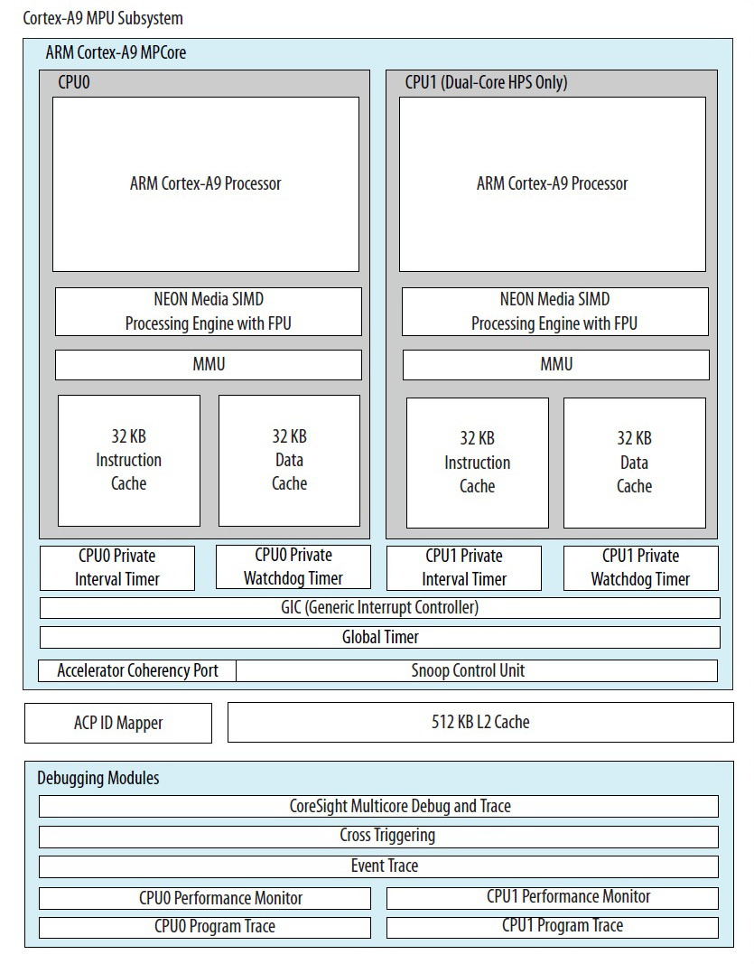
If you had to solve the problem of launching two different programs on two cores, then it will be useful for you to know how to enable MMU and Cache for both cores. Without this, any program is more difficult than blinking an LED, it will run extremely slowly.
MMU and Cache for the first core
#include "alt_cache.h"
#include "alt_mmu.h"
/* MMU Page table - 16KB aligned at 16KB boundary */
#define ARRAY_SIZE(array) (sizeof(array) / sizeof(array[0]))
static uint32_t __attribute__ ((aligned (0x4000))) alt_pt_storage[4096];
static void *alt_pt_alloc(const size_t size, void *context)
static void mmu_init(void)
{
    uint32_t *ttb1 = NULL;
        // Populate the page table with sections (1 MiB regions).
        ALT_MMU_MEM_REGION_t regions[] = {
                // Memory area: 4 mb
                {
                    .va         = (void *)0x00000000,
                    .pa         = (void *)0x00000000,
                    .size       = 0x00400000,
                    .access     = ALT_MMU_AP_PRIV_ACCESS,
                    .attributes = ALT_MMU_ATTR_WBA,
                    .shareable  = ALT_MMU_TTB_S_SHAREABLE,
                    .execute    = ALT_MMU_TTB_XN_DISABLE,
                    .security   = ALT_MMU_TTB_NS_SECURE
                },
                // Device area: Everything else
                {
                    .va         = (void *)0x00400000,
                    .pa         = (void *)0x00400000,
                    .size       = 0xffc00000,
                    .access     = ALT_MMU_AP_PRIV_ACCESS,
                    .attributes = ALT_MMU_ATTR_DEVICE_NS,
                    .shareable  = ALT_MMU_TTB_S_NON_SHAREABLE,
                    .execute    = ALT_MMU_TTB_XN_ENABLE,
                    .security   = ALT_MMU_TTB_NS_SECURE
                }
        };
        alt_mmu_init();
        alt_mmu_va_space_storage_required(regions, ARRAY_SIZE(regions));
        alt_mmu_va_space_create(&ttb1, regions, ARRAY_SIZE(regions), alt_pt_alloc, alt_pt_storage);
        alt_mmu_va_space_enable(ttb1);
}
int main()
{
	mmu_init();
	alt_cache_system_enable();
}
This is how the code for the first core looks. Since the MMU and the Data and Instruction Cache are different for each core, in the code for the second core it is necessary to write a similar MMU initialization function and enable only the corresponding caches, since L2 is already initialized by the first core.
MMU and Cache for the second core
int main_cpu1()
{
      mmu_init2();
      alt_cache_l1_enable_all();
}
This configuration works for sure.
It is worth saying a few words about interrupts. Everything is trivial here, first turn on the GIC (it is enough to do this only on the first core once), then in each core you need to separately initialize and enable the interrupt purely for the CPU. Functions are used for this.
alt_int_global_init();
alt_int_global_enable();
alt_int_cpu_init();
alt_int_cpu_enable();
Upon the occurrence of interruptions, the counter must go on the desired vector, which can be declared only once. For this reason, the initialization of the second core also starts from the VECTORS area, and then passes through the condition to the start_cpu1 file. Because otherwise it would be necessary to re-declare the same vectors with the same names, but this cannot be done in one project.
In general, I even tried to make an extreme “perversion”. Created and compiled two completely different projects, but placed the code in different places so that there was no overlap. Converted .axf to .bin. In the code of the first kernel, I configured the counter address exactly in the place of main () of the code of the second core. Then, through Hex, the editor sewed two files into one, with the correct placement of the code at the address. Everything worked, but somehow shitty. Yes, and debugging such a miracle is not at all convenient. I suspected it was a bad idea, but it was just interesting to check. That's all for me, thanks to everyone who read!
Literature
- In general, look for all the detailed information about scatter syntax in the documents of the version of ARM Compiler armlink User Guide you need .
- About assembler in the ARM Compiler armasm User Guide .