May 27, 2017 at 3:22
 A bit of reverse engineering USB flash on the SK6211 controller
Recently, discussing the nuances of USB flash on this resource, I came across the fact that the majority of technically literate people, due to the lack of literature, have no idea about the basic principles of NAND controllers, and therefore there are a lot of statements that are far from reality about the features of optimizing device firmware , or wrong conclusions are made about the reasons for the failure of the devices themselves.
In order to dispel the illusions a little, we will try using reverse engineering methods to analyze the operation algorithms of the NAND controller manufactured by SKYMEDI SK6211 using the example of a finished product in the form of USB flash 8Gb, released by Kingston.

fig. 1
For a full analysis, we first create a simulation of the use of the drive by recording a large number of files, followed by partial random deletion and re-recording. Next, we write half the LBA of the range with zeros, but in addition to zeros, we place at each offset in the 0x0 DWORD with its number. We write the second half of the logical range with the 0x77 pattern (this pattern is relatively convenient for analyzing data noisy algorithms).
Solder both NAND flash memory chips. In this instance they are made by Samsung, marking K9HBG08U1M by TSOP-48. Operational characteristics: page size - 2112 bytes, block size - 128 pages, number of blocks in a plane - 2048, number of planes in a bank - 4, number of physical banks - 2. Total capacity of two microcircuits 2112 * 128 * 2048 * 4 * 2 * 2 = 8 858 370 048 bytes.

fig. 2
In fig. 2 shows the principle of numbering blocks (a block consists of 128 pages). It is worth noting that this chip can simultaneously perform programming / erasing operations in two planes at once (variations of 0.1 and 2.3). Those who wish to study in more detail the features of microcircuits and the nuances of working with them can look for technical documentation (datasheet), which is currently already available to the general public K9HBG08U1M.pdf.
To read the microcircuits, we use the NAND reader, which is part of the Flash Extractor complex. In those days, when the SK6211 controller was popular, this complex, designed for data recovery, was almost the only analytical tool that was available for sale.

fig. 3
Starting to analyze the data distribution algorithms by the SK6211 controller, we learn about its possibilities of parallel operation with microcircuits from advertising sources, as well as about slightly different two types of error correction codes (ECC). In this publication, due to the vastness of the topic, we omit the description of the features of the error correction codes, and the entire mathematical component associated with them.
The first task in the data analysis is to establish signs of noisy data being written to memory. To do this, search for the 0x77 pattern we recorded and try to find many pages that are completely filled with it. But the search results do not lead to success, which allows us to conclude that the data are recorded in an altered form. When scrolling through dumps, we find a large number of pages filled with the value 0x88 except the last 64 bytes, as well as a large number of pages filled entirely with 0xFF except 4 bytes at the beginning of each 512 byte block and the last 64 bytes (within the boundaries of the page 2112 bytes). Based on what patterns we recorded on USB flash, we will assume that there is data inversion. Before performing data inversion, we will analyze the contents of NAND pages to determine the location of service data.

Figure 4.
SK6211 in the used pages allocates 2048 bytes of data ( DA ) and allocates 64 bytes to store service data ( SA ). 4 groups of data of 16 bytes are well traced, which hints at their applicability to four blocks of 512 contained in the page.
List the contents of the first 16-byte group of several thousand pages.

fig. 5
In fig. Figure 5 shows that the first 4 bytes remain ordered, and the chaotic content is located in the remaining 12. Based on this, it can be assumed that the last 12 bytes in each row contain an error correction code. Knowing that the block with which the NAND chip operates is 128 pages, we will calculate the block size 2112 * 128 = 270 336 (0x42000) bytes. From 0x00108000 we’ll take one block forward, that is, to the page at 0x0014a000.

fig. 6
from the contents of Fig. 5 and fig. 6 it is obvious that the 3rd byte plays the role of the page number for the NAND memory block. This assumption is not refuted when viewing all non-empty blocks of NAND memory.
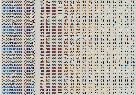
fig. 7
At 0 and 1 bytes of service data in each page for two blocks the same values. It can be assumed that this pair of bytes is reserved for the block number. We derive all the values for all blocks and find that in the lower nibble of the first byte, values from 0x0 to 0x3 are used, and in the zero byte, values from 0x00 to 0xFF run through. The high nibble values in the first byte have more diverse meanings. Suppose that 10 bits are used for numbering, which are formed from the two least significant bits of the first byte of the service area as the high part and 8 bits from the zero byte as the low part. We check the accuracy of the assumptions by displaying the numbers for the first 0x400 blocks. Sorting them in ascending order, we note that a chain of numbers from 0x000 to 0x3C3 is built sequentially, which confirms the correctness of the assumption. Performing similar checks for the remaining groups of 0x400 blocks, we finally exclude the possibility of an erroneous interpretation.
We perform data inversion, with the exception of service data, and analyze the data parallelization mechanism. Let's check the assumption about the symmetry of recording in different banks by analyzing the logical numbers in the blocks in each dump. In the case of SK6211, the assumption of symmetrical recording is confirmed. Find a block with a logical number 0x000, in which each 512 data block contains a serial number and zeros as content. Based on the actual location of the data recorded by us, we will build a table of the position of the data.
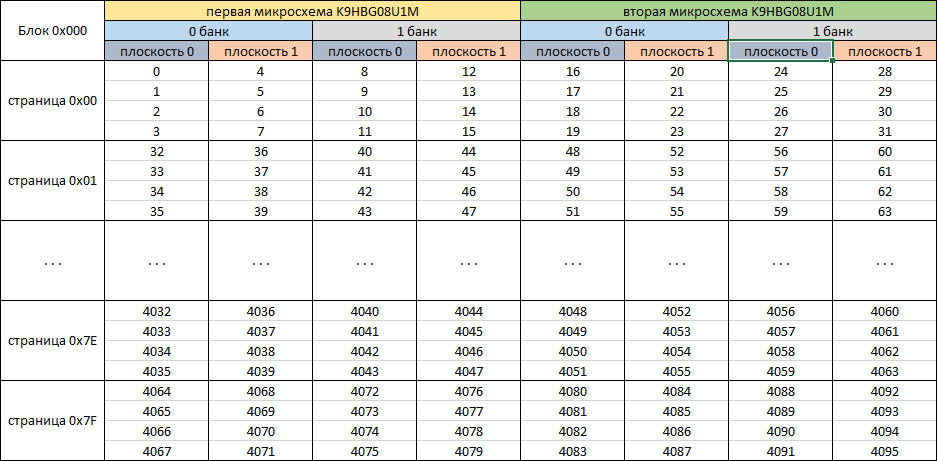
Fig. 8
According to the data placement, we can notice that the controller for this chipset implements the most efficient parallelization to obtain high performance. Taking into account the data parallelization mechanism, we calculate the block size that the translation system operates in the drive microcode 0x42000 * 8 = 0x210000 bytes. If we discard the service data, then the block size is 0x40000 * 8 = 0x200000 (2 097 152) bytes.
For further analysis, we need to eliminate the spread of data and collect them into whole blocks of 2 MB.
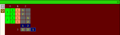
fig. 9
The first step is the elimination of parallelization between the planes by paginating the even and odd blocks.
The second step is to combine the doubled page size of 0 and 1 banks of each of the NAND memory chips.
The third step is to combine the quad-page size of both NAND memory chips.
When analyzing the contents of 2MB blocks in the resulting dump, a monotonously increasing sequence of numbered "sectors" is observed, which confirms the correctness of the analysis of the data parallelization algorithm.
Next, at the precast dump, we will find out the arrangement of blocks and organization into logical banks.

Fig. 10 We will
search for several dozen blocks and collect by serial number. Based on the results of the collection, we make sure that our numbering of sectors in the blocks is joined. And the earlier assumption that 10 bits of the first two overhead bytes are the block number is true.
The total chip size is 8 858 370 048 (0x210000000) bytes the block size in the translator is 2 162 688 (0x210000). Total blocks 0x210000000 / 0x210000 = 0x1000 (4096). Based on the digit capacity of the numbers used and the actual numbering, the block numbers cannot exceed 0x400 (1024) from this we can conclude that there are 4 logical banks in the broadcast. We conditionally divide the resulting dump into 4 equal parts (0x400 blocks each), estimate the block numbers in each part, and based on this, assume the number of blocks included in the broadcast in each logical bank.

fig. 11
Note that the size of each logical bank is noticeably smaller than 0x400. This need is dictated by the fact that "extra" blocks in some quantities are needed for service structures and, most importantly, for the effective operation of the wear leveling mechanism. The mechanism is implemented on the principle that each block in which the content is changed will be excluded from the broadcast and will fall into the backup, and its place will be taken by the block, which was not included in the broadcast before recording the changed data and was considered a backup. Given the counters of recording in each block, the mechanism works quite effectively. The Achilles heel of this algorithm will be an abundance of unchanged data, then a relatively small number of blocks will be involved in recordings in rotation.
This principle is very clearly confirmed by the location of the blocks in the dump. According to fig. 10 you can see how non-linear the scatter of the blocks from which the logical space is realized. Soldering the NAND memory chips back and connecting the USB flash to the computer, perform a number of records in the first 4096 “sectors”, again drop out and read the NAND memory chips, collect and evaluate the order of blocks in the resulting dump.

fig. 12
As we can see, with the remaining blocks unchanged, the block with logical number 0x000 “migrated” to another place. At the old address, all the pages of the block, both in the user data area and in the service area, are completely filled with 0xFF, which indicates that this block is cleared and excluded from translation.
Comparing both resulting dumps, in addition to the changed data in the zero block there will be changes in the service data, analyzing which we can establish how the structure of the translator is formed.
Such an analysis method allows you to get enough data about the operation algorithm of the USB NAND controller to use it to recover information from damaged drives based on the controller under study, and also allows you to see in action the mechanisms of data parallelization and wear leveling. Also, based on the translator’s device and USB flash analysis (additional analysis is carried out on a drive formatted in FAT32 and filled with several thousand files), you can notice that for blocks with file system structures there is no privileged allocation of blocks.
Next post: Recovering Data from a Seagate FreeAgent Go External Hard Drive
Previous post: Recovering data from a damaged RAID 5 array in a Linux-based NAS
In order to dispel the illusions a little, we will try using reverse engineering methods to analyze the operation algorithms of the NAND controller manufactured by SKYMEDI SK6211 using the example of a finished product in the form of USB flash 8Gb, released by Kingston.
fig. 1
For a full analysis, we first create a simulation of the use of the drive by recording a large number of files, followed by partial random deletion and re-recording. Next, we write half the LBA of the range with zeros, but in addition to zeros, we place at each offset in the 0x0 DWORD with its number. We write the second half of the logical range with the 0x77 pattern (this pattern is relatively convenient for analyzing data noisy algorithms).
Solder both NAND flash memory chips. In this instance they are made by Samsung, marking K9HBG08U1M by TSOP-48. Operational characteristics: page size - 2112 bytes, block size - 128 pages, number of blocks in a plane - 2048, number of planes in a bank - 4, number of physical banks - 2. Total capacity of two microcircuits 2112 * 128 * 2048 * 4 * 2 * 2 = 8 858 370 048 bytes.
fig. 2
In fig. 2 shows the principle of numbering blocks (a block consists of 128 pages). It is worth noting that this chip can simultaneously perform programming / erasing operations in two planes at once (variations of 0.1 and 2.3). Those who wish to study in more detail the features of microcircuits and the nuances of working with them can look for technical documentation (datasheet), which is currently already available to the general public K9HBG08U1M.pdf.
To read the microcircuits, we use the NAND reader, which is part of the Flash Extractor complex. In those days, when the SK6211 controller was popular, this complex, designed for data recovery, was almost the only analytical tool that was available for sale.
fig. 3
Starting to analyze the data distribution algorithms by the SK6211 controller, we learn about its possibilities of parallel operation with microcircuits from advertising sources, as well as about slightly different two types of error correction codes (ECC). In this publication, due to the vastness of the topic, we omit the description of the features of the error correction codes, and the entire mathematical component associated with them.
The first task in the data analysis is to establish signs of noisy data being written to memory. To do this, search for the 0x77 pattern we recorded and try to find many pages that are completely filled with it. But the search results do not lead to success, which allows us to conclude that the data are recorded in an altered form. When scrolling through dumps, we find a large number of pages filled with the value 0x88 except the last 64 bytes, as well as a large number of pages filled entirely with 0xFF except 4 bytes at the beginning of each 512 byte block and the last 64 bytes (within the boundaries of the page 2112 bytes). Based on what patterns we recorded on USB flash, we will assume that there is data inversion. Before performing data inversion, we will analyze the contents of NAND pages to determine the location of service data.
Figure 4.
SK6211 in the used pages allocates 2048 bytes of data ( DA ) and allocates 64 bytes to store service data ( SA ). 4 groups of data of 16 bytes are well traced, which hints at their applicability to four blocks of 512 contained in the page.
List the contents of the first 16-byte group of several thousand pages.
fig. 5
In fig. Figure 5 shows that the first 4 bytes remain ordered, and the chaotic content is located in the remaining 12. Based on this, it can be assumed that the last 12 bytes in each row contain an error correction code. Knowing that the block with which the NAND chip operates is 128 pages, we will calculate the block size 2112 * 128 = 270 336 (0x42000) bytes. From 0x00108000 we’ll take one block forward, that is, to the page at 0x0014a000.
fig. 6
from the contents of Fig. 5 and fig. 6 it is obvious that the 3rd byte plays the role of the page number for the NAND memory block. This assumption is not refuted when viewing all non-empty blocks of NAND memory.
fig. 7
At 0 and 1 bytes of service data in each page for two blocks the same values. It can be assumed that this pair of bytes is reserved for the block number. We derive all the values for all blocks and find that in the lower nibble of the first byte, values from 0x0 to 0x3 are used, and in the zero byte, values from 0x00 to 0xFF run through. The high nibble values in the first byte have more diverse meanings. Suppose that 10 bits are used for numbering, which are formed from the two least significant bits of the first byte of the service area as the high part and 8 bits from the zero byte as the low part. We check the accuracy of the assumptions by displaying the numbers for the first 0x400 blocks. Sorting them in ascending order, we note that a chain of numbers from 0x000 to 0x3C3 is built sequentially, which confirms the correctness of the assumption. Performing similar checks for the remaining groups of 0x400 blocks, we finally exclude the possibility of an erroneous interpretation.
We perform data inversion, with the exception of service data, and analyze the data parallelization mechanism. Let's check the assumption about the symmetry of recording in different banks by analyzing the logical numbers in the blocks in each dump. In the case of SK6211, the assumption of symmetrical recording is confirmed. Find a block with a logical number 0x000, in which each 512 data block contains a serial number and zeros as content. Based on the actual location of the data recorded by us, we will build a table of the position of the data.
Fig. 8
According to the data placement, we can notice that the controller for this chipset implements the most efficient parallelization to obtain high performance. Taking into account the data parallelization mechanism, we calculate the block size that the translation system operates in the drive microcode 0x42000 * 8 = 0x210000 bytes. If we discard the service data, then the block size is 0x40000 * 8 = 0x200000 (2 097 152) bytes.
For further analysis, we need to eliminate the spread of data and collect them into whole blocks of 2 MB.
fig. 9
The first step is the elimination of parallelization between the planes by paginating the even and odd blocks.
The second step is to combine the doubled page size of 0 and 1 banks of each of the NAND memory chips.
The third step is to combine the quad-page size of both NAND memory chips.
When analyzing the contents of 2MB blocks in the resulting dump, a monotonously increasing sequence of numbered "sectors" is observed, which confirms the correctness of the analysis of the data parallelization algorithm.
Next, at the precast dump, we will find out the arrangement of blocks and organization into logical banks.
Fig. 10 We will
search for several dozen blocks and collect by serial number. Based on the results of the collection, we make sure that our numbering of sectors in the blocks is joined. And the earlier assumption that 10 bits of the first two overhead bytes are the block number is true.
The total chip size is 8 858 370 048 (0x210000000) bytes the block size in the translator is 2 162 688 (0x210000). Total blocks 0x210000000 / 0x210000 = 0x1000 (4096). Based on the digit capacity of the numbers used and the actual numbering, the block numbers cannot exceed 0x400 (1024) from this we can conclude that there are 4 logical banks in the broadcast. We conditionally divide the resulting dump into 4 equal parts (0x400 blocks each), estimate the block numbers in each part, and based on this, assume the number of blocks included in the broadcast in each logical bank.
fig. 11
Note that the size of each logical bank is noticeably smaller than 0x400. This need is dictated by the fact that "extra" blocks in some quantities are needed for service structures and, most importantly, for the effective operation of the wear leveling mechanism. The mechanism is implemented on the principle that each block in which the content is changed will be excluded from the broadcast and will fall into the backup, and its place will be taken by the block, which was not included in the broadcast before recording the changed data and was considered a backup. Given the counters of recording in each block, the mechanism works quite effectively. The Achilles heel of this algorithm will be an abundance of unchanged data, then a relatively small number of blocks will be involved in recordings in rotation.
This principle is very clearly confirmed by the location of the blocks in the dump. According to fig. 10 you can see how non-linear the scatter of the blocks from which the logical space is realized. Soldering the NAND memory chips back and connecting the USB flash to the computer, perform a number of records in the first 4096 “sectors”, again drop out and read the NAND memory chips, collect and evaluate the order of blocks in the resulting dump.
fig. 12
As we can see, with the remaining blocks unchanged, the block with logical number 0x000 “migrated” to another place. At the old address, all the pages of the block, both in the user data area and in the service area, are completely filled with 0xFF, which indicates that this block is cleared and excluded from translation.
Comparing both resulting dumps, in addition to the changed data in the zero block there will be changes in the service data, analyzing which we can establish how the structure of the translator is formed.
Such an analysis method allows you to get enough data about the operation algorithm of the USB NAND controller to use it to recover information from damaged drives based on the controller under study, and also allows you to see in action the mechanisms of data parallelization and wear leveling. Also, based on the translator’s device and USB flash analysis (additional analysis is carried out on a drive formatted in FAT32 and filled with several thousand files), you can notice that for blocks with file system structures there is no privileged allocation of blocks.
Next post: Recovering Data from a Seagate FreeAgent Go External Hard Drive
Previous post: Recovering data from a damaged RAID 5 array in a Linux-based NAS