We look at the insides of the domestic 28nm MIPS processor - Baikal-T1
 I think many have already heard about the Baikal-T1 processor implemented by Moscow Baikal Electronics developers - with two Imagination Technologies P5600 MIPS 32 r5 cores and on-board 10GbE. Baikal was the first to implement this core in silicon.
 I tormented this processor with interruptions for more than a year - but finally under the cut I can share the results.
Attention, the pictures are clickable - but in some places they are quite heavy (up to 100Mb).
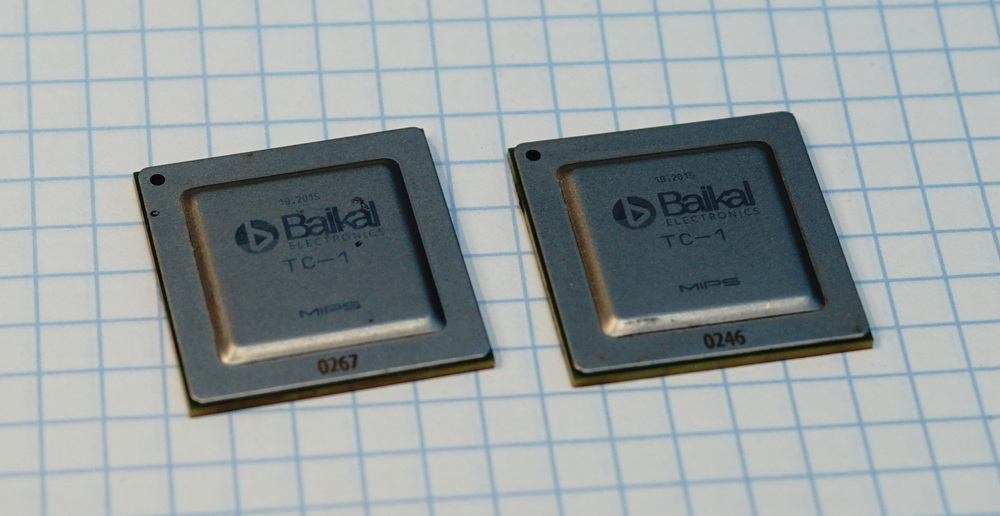
The processors themselves (4 of them had to be opened): the
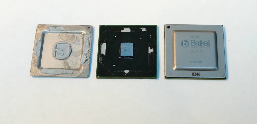
BGA substrate and the heat-distributing / protective cover - like other modern processors (Intel and co), the chip is turned upside down (flip-chip BGA):
The crystal itself has the entire area contacts, most of which are for powering the entire chip area. This is necessary not so much because of the high energy consumption (it is just low, ≤5W), but to reduce the inductance of the power circuits. Again, most modern processors have a similar power system: On the left side is an Ethernet controller (probably 10GbE KR / KX4), half is visible on the frame:

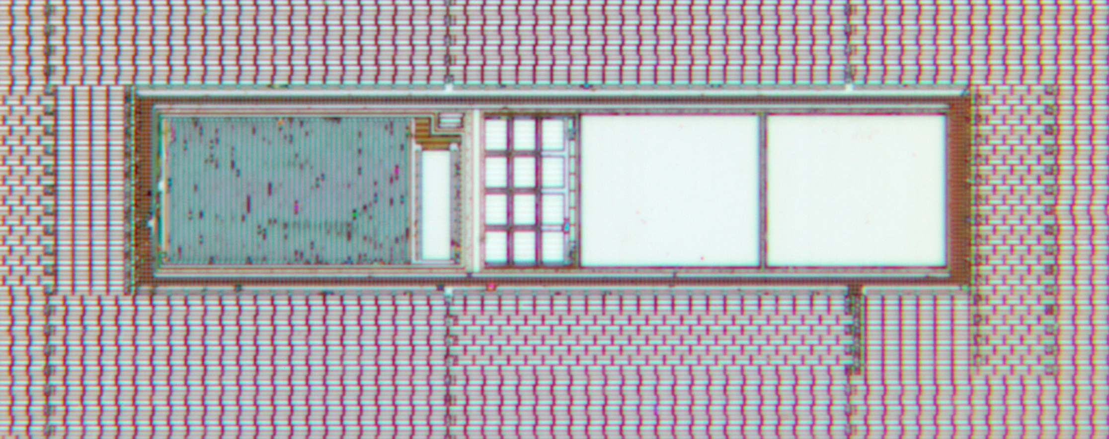
After removing the metallization, we see the logic autosynthesized from standard cells ( Multiclet, for example, was synthesized by 180nm with the same “waves”), a bunch of generated memory instances / register files (usually supplied by the factory), and identical monitoring units (presumably small white blue vertical rectangles). A noticeable part of the chip (about 25%) is not occupied by transistors, and there it is simply filling with empty cells. Let's look a little closer: Presumably, a monitoring unit (temperature / inverter chain generation speed for example). Around is a field of empty cells:

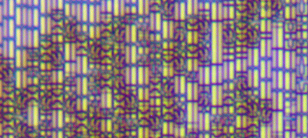
Rows of standard cells in maximum optical resolution. Here 1 pixel = 28.5nm, 28 micrometers (0.03mm) per frame width, but the optical resolution is limited by diffraction at the level of about 200nm (because the frame seems and is fuzzy). It can be seen that, in a first approximation, the approach is the same as that at 180 nm - the same rows of back-to-back transistors are [PN] [NP] [PN] ... transistors (i.e. adjacent rows of standard cells are mirrored ) The line with P transistors is slightly wider:
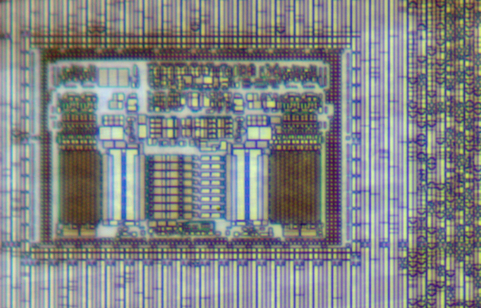
One of the small generated blocks of memory - the SRAM array of cells itself occupies a small part of the block (the rest are line / column drivers and signal amplifiers, external interface logic). Around in more detail the field of “empty” cells is visible (absolutely nothing can be drawn there - the chip will turn out to be uneven in height, which is unacceptable):
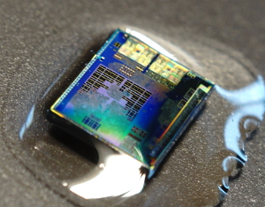
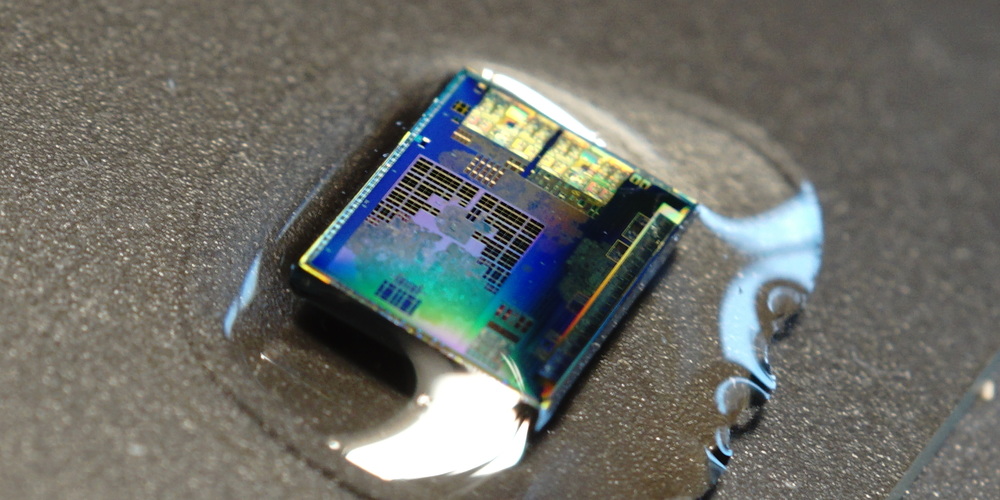
Finally - a photograph of Baikal in immersion oil, immediately after the last shots:
In my opinion, Baikal-T1 is a big step forward for domestic civilian microelectronics. This is a modern core, developed and manufactured using modern mass civil technologies, which solves the tasks by standard means - the development route generally accepted in the world industry, an understandable and open compiler for everyone, an understandable and open OS. Inventing your bicycles where you can do without them is a real scourge of domestic developments, and this was avoided.
That's all for now - I hope to publish more often in the foreseeable future. If you like this kind of work - now you can support them on Patreon or in other ways (and there you look and get to the electron microscope / FIB).