December 9, 2016 at 02:40
Implementation of PCI Express v3.0 x16 on Virtex 7 FPGA
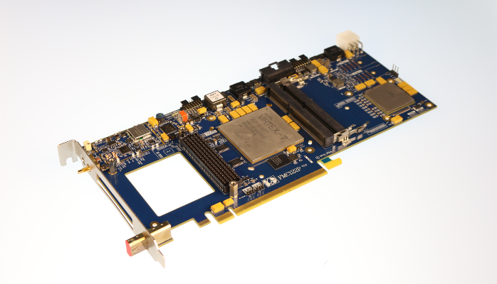
Computers have long had a PCI Express v3.0 x16 bus; Tests of modern video adapters show a speed of about 12 GB / s on this bus. I would like to make a module on the FPGA that has the same speed. However, available FPGAs have a HARDWARE controller for PCIe v3.0 x8 only; Implementations of SOFT IP Core are, but very expensive. But there is a way.
FPGA Virtex 7 VX330T has two PCI Express v3.0 x8 controllers; The obvious solution is to place a switch that has x16 on the side of the connector and two x8 buses that are connected to the FPGA. It turns out this structure:
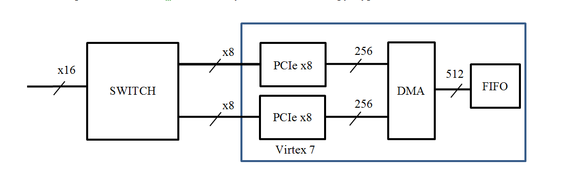
According to this scheme, the HTG-728 module of HighTechGlobal is built.
The Alpha-Data company follows a different path. The ADM-PCIE-KU3-X16 does not have a switch. But on the x16 connector, two x8 buses are output. In FPGA, it is possible to implement two independent controllers. For this, two reset signals and two reference frequencies are set up on the FPGA. But this module will work only in special motherboards, where two x8 are also output to the x16 connector. I have not seen such motherboards, but apparently they are.
Our company decided to implement the FMC122P module with an internal switch. The main task was to check the maximum exchange rate. Another, no less important task, is to achieve compatibility with existing software and FPGA components.
The PCI Express controller for Virtex 7 is fundamentally different from the controllers for Virtex 6, Kintex 7. It has become more convenient, but it is different. The figure shows the block diagram of the controller:

The controller has two parts, Completer and Requester, each of which has two AXI_Stream buses. The Completer node receives requests from the PCI Express bus. These requests are sent to the m_axis_cq bus. On the bus s_axis_cc, a response from the User component should come. Usually this is the access point to the internal FPGA registers.
Through the Requester node on the s_axis_rq bus, the DMA sends requests to the PCI Express bus. Responses come via the m_axis_rc bus.
Tire simulation
The composition of IP Core includes an example project by which you can understand how it works. The project is written in Verilog and, unfortunately, it can also serve as an example of how not to develop. Let's look at a block diagram of an example.
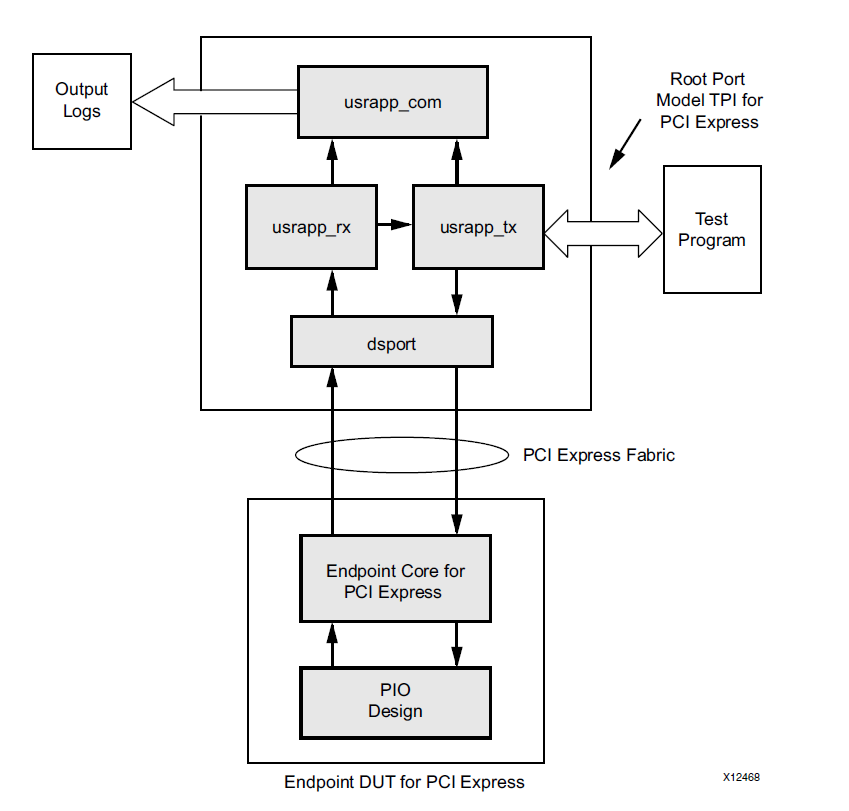
This diagram is from the IP Core description. At first glance, everything is fine - this is a wonderful picture, it can be shown to managers, project managers, clients. Problems begin in implementation. There are many places in this system where Verilog features are used to access objects along an absolute path. In my opinion, in this system this is justified only in one place - this is a bypass of GTP nodes for modeling at the PIPE level. But to make a connection between userapp_tx and userapp_rx using absolute paths is completely unnecessary.
In the project, it looks like this:
The pci_exp_usrapp_tx component has a TSK_SYSTEM_INITIALIZATION function that calls the pci_exp_userapp_cfg function through the absolute path:
board.RP.cfg_usrapp.TSK_WRITE_CFG_DW (hereinafter I call the function what Verilog describes through task). We look at the pci_exp_userapp_cfg component, what we see: cfg_ds_bus_number <= board.RP.tx_usrapp.RP_BUS_DEV_FNS [15: 8];
We look at the pci_exp_userapp_rc component, the same thing there: board.RP.com_usrapp.TSK_PARSE_FRAME (`RX_LOG);
This is not only stylistically incorrect. This makes it difficult to apply the model in your project. Firstly, it’s not necessary that in your own project the top-level file will be called board and the same hierarchy will remain there. Secondly, there may be two components. We just happened both cases. I had to work with Verilog, although I did not like it at all. As it turned out, by a small permutation, the entire root_port component can be reduced to a completely hierarchical view. The result is component files:
- xilinx_pcie_3_0_7vx_rp_m2.v
- pci_exp_usrapp_tx_m2.v
- pci_exp_usrapp_cfg_m2.v
And files with functions:
- task_bar.vh
- task_rd.vh
- task_s1.vh
- task_test.vh
This allowed the inclusion of two root_port components in the model. In the VHDL component, the inclusion of two root_port looks like this:
root_port
gen_rp0: if( is_rp0=1 ) generate
rp0: xilinx_pcie_3_0_7vx_rp_m2
	generic map(
		INST_NUM		=> 0
	)
	port map(
		sys_clk_p		=> sys_clk_p,
		sys_clk_n		=> sys_clk_n,
		sys_rst_n		=> sys_rst_n,
  		-- Передача команд
 	  	cmd_rw			=> cmd_rw, 			-- Признак чтения-записи: 0 - чтение, 1 - запись
 	   	cmd_req			=> cmd_req, 		-- 1 - Запрос операции
 	   	cmd_ack			=> cmd_ack, 		-- 1 - подтверждение опреации
 	   	cmd_adr			=> cmd_adr, 		-- адрес для команды чтения-записи
 	   	cmd_data_i		=> cmd_data_i, 		-- данные для записи
 	   	cmd_data_o		=> cmd_data_o, 		-- прочитанные данные
 	   	cmd_init_done 	=> cmd_init_done_0 	-- 1 - инициализация завершена
	);
end generate;
gen_rp1: if( is_rp1=1 ) generate
rp1: xilinx_pcie_3_0_7vx_rp_m2
	generic map(
		INST_NUM		=> 1
	)
	port map(
		sys_clk_p		=> sys_clk_p,
		sys_clk_n		=> sys_clk_n,
		sys_rst_n		=> sys_rst_n,
 	   	cmd_init_done 	=> cmd_init_done_1 	-- 1 - инициализация завершена
	);
end generate;
Through the rp0 component, calls are made to write or read 32-bit words. The rp1 component only performs initialization.
Unfortunately, this is simulated for a very long time, even if the simulation is carried out at the PIPE level. A typical modeling session is about ten minutes (and maybe more, I don’t remember anymore). For operational work with a DMA channel, this is not suitable. In this situation, a completely natural decision was made to remove the PCI Express controller from the model. Moreover, it has already been studied.
Block diagram of the controller
A generalized diagram of the controller is shown in the figure.
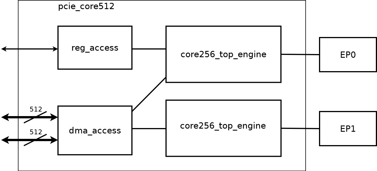
Two identical core256_top_engine components provide access to two EP0, EP1 controllers. core256_top_engine provides access to registers from the side of PCI Express, for this only EP0 and the reg_access component are used. The dma_access component contains the main controller control logic. Its block diagram is shown in the figure below: The
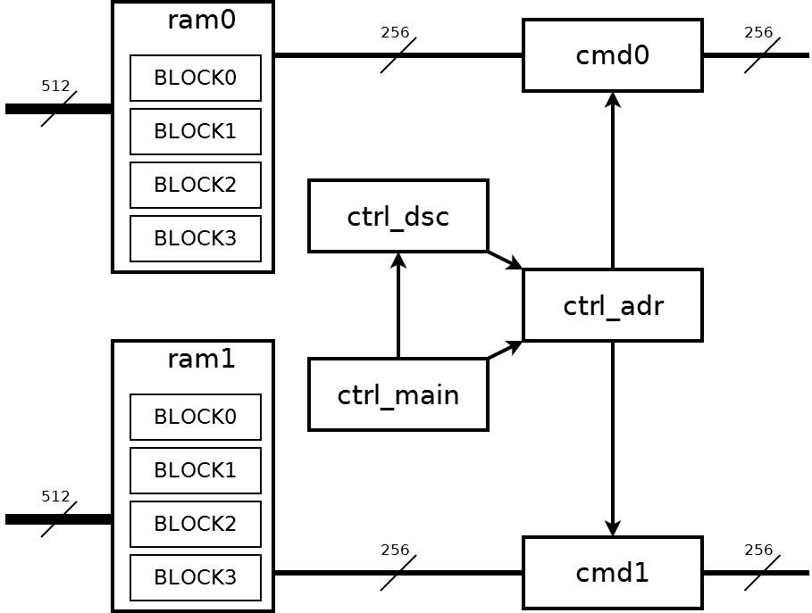
ctrl_main node controls everything. The ctrl_dsc node contains a descriptor block. The ctrl_adr node converts the descriptor into a sequence of four-kilobyte block addresses. Addresses are sent to cmd0 and cmd1 nodes for exchange with core256_top_engine nodes;
On the user side of the FPGA, there are two buses with a width of 512 bits. But data on these buses must be transmitted in blocks of 4 kilobytes and strictly in turn. This is required to populate the memory nodes ram0, ram1 in turn. Each memory node contains four blocks of 4 kilobytes. On these memory nodes, the original 512-bit stream splits into two 256-bit streams. In the future, two 256-bit streams are already completely independent. Data flows will be found only in the computer's RAM, where they will be at neighboring addresses.
Modeling dma_access
The dma_access node is the most complex part of the controller. Accordingly, it must be modeled especially carefully. As I wrote above, simulating two PCI Express cores takes a very long time. To speed up, a model has been developed that connects instead of core256_top_engine. The same interface remained for dma_access, and the modeling speed increased by an order of magnitude. In this project, as well as in the PROTEQ project, automatic start of tests through a tcl file is used.
Here is a snippet of the tcl file:
run_test "stend_m4" "test_read_8kb        "   	6  "50 us"
run_test "stend_m4" "test_read_16kb       "   	7  "100 us"
run_test "stend_m4" "test_read_49blk      "   	8  "150 us"
run_test "stend_m4" "test_read_8x4_cont   "   	9  "150 us"
run_test "stend_m4" "test_read_128x1_cont "   	12 "200 us"
run_test "stend_m4" "test_read_16kbx2     "   	13 "150 us"
run_test "stend_m4" "test_read_step       "   	14 "200 us"
run_test "stend_m4" "test_read_8kb_sg_eot "		15 "100 us"
run_test "stend_m4" "test_read_64x1       "		16 "100 us"
This is an automatic run of nine tests. For example, I’ll give the code for one test:
test_read_4kb
procedure test_read_4kb (
		signal  cmd:	out bh_cmd; --! команда
		signal  ret:	in  bh_ret  --! ответ
		)
is
variable	adr				: std_logic_vector( 31 downto 0 );
variable	data			: std_logic_vector( 31 downto 0 );
variable	str				: line;
variable 	L 				: line;
variable	error			: integer:=0;
variable	dma_complete	: integer;
variable	data_expect		: std_logic_vector( 31 downto 0 );
begin
	write( str, string'("TEST_READ_4KB" ));
	writeline( log, str );
	---- Формирование блока дескрипторов ---
	for ii in 0 to 127 loop
		adr:= x"00100000";
		adr:=adr + ii*4;
		int_mem_write( cmd, ret, adr,  x"00000000" );
	end loop;
	int_mem_write( cmd, ret, x"00100000",  x"00008000" );
	int_mem_write( cmd, ret, x"00100004",  x"00000100" );
--	int_mem_write( cmd, ret, x"00100080",  x"00008000" );
--	int_mem_write( cmd, ret, x"00100084",  x"00000100" );
	int_mem_write( cmd, ret, x"001001F8",  x"00000000" );
	int_mem_write( cmd, ret, x"001001FC",  x"762C4953" );
	---- Программирование канала DMA ----
	block_write( cmd, ret, 4, 8, x"00000025" );		-- DMA_MODE
	block_write( cmd, ret, 4, 9, x"00000010" );		-- DMA_CTRL - RESET FIFO
	block_write( cmd, ret, 4, 20, x"00100000" );	-- PCI_ADRL
	block_write( cmd, ret, 4, 21, x"00100000" );	-- PCI_ADRH
	block_write( cmd, ret, 4, 23, x"0000A400" );	-- LOCAL_ADR
	block_write( cmd, ret, 4, 9, x"00000001" );		-- DMA_CTRL - START
	wait for 20 us;
	block_read( cmd, ret, 4, 16, data );			-- STATUS
	write( str, string'("STATUS: " )); hwrite( str, data( 15 downto 0 ) );
	if( data( 8 )='1' ) then
		write( str, string'(" - Дескриптор правильный" ));
	else
		write( str, string'(" - Ошибка чтения дескриптора" ));
		error := error + 1;
	end if;
	writeline( log, str );
	if( error=0 ) then
		---- Ожидание завершения DMA ----
		dma_complete := 0;
		for ii in 0 to 100 loop
		block_read( cmd, ret, 4, 16, data );			-- STATUS
		write( str, string'("STATUS: " )); hwrite( str, data( 15 downto 0 ) );
			if( data(5)='1' ) then
				write( str, string'(" - DMA завершён " ));
				dma_complete := 1;
			end if;
			writeline( log, str );
			if( dma_complete=1 ) then
				exit;
			end if;
			wait for 1 us;
		end loop;
		writeline( log, str );
		if( dma_complete=0 ) then
			write( str, string'("Ошибка - DMA не завершён " ));
			writeline( log, str );
			error:=error+1;
		end if;
	end if;
	for ii in 0 to 3 loop
		block_read( cmd, ret, 4, 16, data );			-- STATUS
		write( str, string'("STATUS: " )); hwrite( str, data( 15 downto 0 ) );
		writeline( log, str );
		wait for 500 ns;
	end loop;
	block_write( cmd, ret, 4, 9, x"00000000" );		-- DMA_CTRL - STOP
	write( str, string'(" Прочитано: " ));
	writeline( log, str );
	data_expect := x"A0000000";
	for ii in 0 to 1023 loop
		adr:= x"00800000";
		adr:=adr + ii*4;
		int_mem_read( cmd, ret, adr,  data );
		if( data=data_expect ) then
			fprint( output, L, "%r : %r  - Ok\n", fo(ii), fo(data));
			fprint( log,    L, "%r : %r  - Ok\n", fo(ii), fo(data));
		else
			fprint( output, L, "%r : %r  Ожидается: %r - Error \n", fo(ii), fo(data), fo(data_expect));
			fprint( log,    L, "%r : %r  Ожидается: %r - Error \n", fo(ii), fo(data), fo(data_expect));
			error:=error+1;
		end if;
		data_expect := data_expect + 1;
	end loop;
--	block_write( cmd, ret, 4, 9, x"00000010" );		-- DMA_CTRL - RESET FIFO
--	block_write( cmd, ret, 4, 9, x"00000000" );		-- DMA_CTRL
--	block_write( cmd, ret, 4, 9, x"00000001" );		-- DMA_CTRL - START
	fprint( output, L, "\nTest time:  %r \n", fo(now) );
	fprint(    log, L, "\nTest time:  %r \n", fo(now) );
	-- вывод в файл --
	writeline( log, str );
	if( error=0 ) then
		write( str, string'("TEST finished successfully" ));
		cnt_ok := cnt_ok + 1;
	else
		write( str, string'("TEST finished with ERR" ));
		cnt_error := cnt_error + 1;
	end if;
	writeline( log, str );
	writeline( log, str );
	-- вывод в консоль --
	writeline( output, str );
	if( error=0 ) then
		write( str, string'("TEST finished successfully" ));
	else
		write( str, string'("TEST finished with ERR" ));
	end if;
	writeline( output, str );
	writeline( output, str );
end test_read_4kb
The int_mem_write commands provide a write to the HOST RAM of the computer. In this test, a descriptor block is written there. The block_write and block_read commands provide access to the controller's DMA registers. The controller is being programmed, its launch and completion of the exchange. After that, the int_mem_read commands read and verify the received data. The code for this test is almost identical to the test from the PCIe_DS_DMA controller, which I published as an open source project on opencores.org; Compared with the original, verification of received data has been added.
Logical organization of the controller
At the register level, the controller repeats our previous controllers for FPGAs Virtex 4, Virtex 5, Virtex 6, Kintex 7; The organization can be found in the PCIe_DS_DMA project.
A feature of all controllers is the union of single descriptors into a block of descriptors. This gives a sharp increase in speed when using fragmented memory.
Connecting to notebooks.
For us it is important to connect this controller to our notebooks. What are notebooks in my previous article: “ADM Interface: What is a notebook” . Working with a 512-bit bus required a change in approach. To connect the notebook, I had to use an additional repacker unit. The block diagram is in the figure.
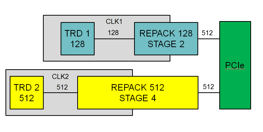
The repacker solves two problems:
- tire tracing on a chip, for this you can set the number of additional stages of the conveyor
- connection to notebooks with 64 and 128 bit buses
Memory usage
The ultimate goal of developing a controller and connecting to notebooks is to obtain a continuous stream of data from the ADC to the computer. And here we are faced with the fact that the PCI Express bus does not provide stable speed. There may be delays on the bus. This is especially noticeable at high metabolic rates. Delays occur due to the operation of other devices. The magnitude of the delay can be different, it can be 5 - 10 μs, or maybe more. A delay of 10 μs at a speed of 11 GB / s corresponds to a memory block of 110 kilobytes. For the internal memory, even modern FPGAs is a lot. But the delay may be longer. If the data stream cannot be suspended, and this is just the case when the ADCs are used, then the only way out is buffering in external memory. Moreover, the memory should be able to work at a speed of 22 GB / s. We have two SODIMM DDR3-1600s installed on the module. The memory operates at a frequency of 800 MHz. This corresponds to a continuous data stream of 8400 MB / s. This figure is confirmed by experiment. I want to note that the speed of 8400 MB / s exceeds the speed of data output from our fastest submodule in which two ADCs at 1800 MHz are installed.
Tracing
The screenshot shows the trace result in the PlanAhead program:
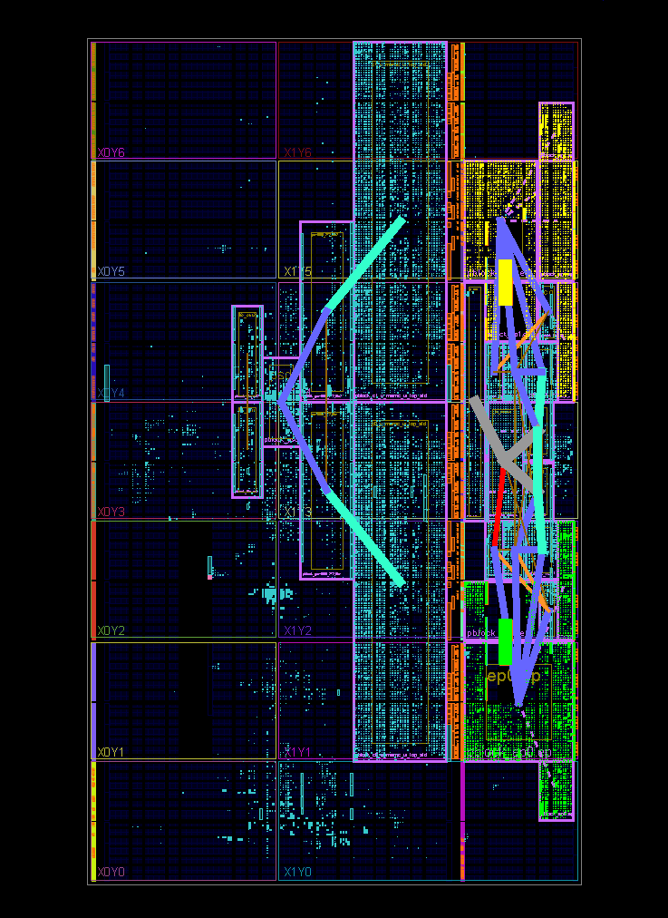
The picture shows two PCI Express controllers (highlighted in yellow and green) and two memory controllers (next to PCI Express).
As it turned out, such a project is very difficult for Vivado, it copes with it very poorly. A project in Vivado is badly bred and often just doesn't work. ISE shows much more stable results. PCI Express nodes were laid out in accordance with the Xilinx recommendations, but it turned out that they were spaced apart on a chip. And this is already creating a problem for sharing the remaining multi-gigabit lines.
Results The
operation of the module was tested on several computers. The results are quite interesting.
| Intel Core i7 4820K | P9X79 WS | DDR3-1866 | 11140 MB / s |
|---|---|---|---|
| Intel Core i7 5820K | X99-A | DDR4-2400 | 11128 MB / s |
| Intel Core i7 3820K | P9X79 | DDR3-1600 | 11120 MB / s |
This is the speed of data entry without verification. The data is continuously entered into a buffer of 1 GB allocated in the system memory area, that is, continuous by physical addresses. Measures the average input speed over an interval of at least 1 minute.
On a computer with DDR3-1600 memory, when the check is turned on, the speed drops to 8500 MB / s.
On a computer with DDR3-1866, the speed does not decrease with one module and the scan turned on.
Two FMC122P modules in a computer with DDR3-1866 without verification also show a maximum speed of about 11,000 MB / s for each module. But when you turn on the test, the speed drops.
For these measurements, it is assumed that 1 MB is 1024 bytes, and 1 KB is 1024 bytes.
I would like to note that in this work I present the result of the work of a large team. Special thanks to Dmitry Avdeev, who did a great job in this project.
PS While development was underway, Virtex 7 managed to become obsolete. Kintex Ultrascale is already more convenient in work. And Kintex Ultrascale + already has a PCI Express v3.0 x16 HARD - so this separation is no longer needed.
PSS But Kintex Ultrascale + also has a PCI Express v4.0 x8 HARD unit - can separation still come in handy?