Server management board - why is it and what's inside
Hello! Maxim is with you again. Today I’ll talk a little about the management board for our server. In general, it does not differ in particular complexity, but it is also impossible to skip this component either - my colleagues and I decided that all the essential subsystems and server components should be illuminated.
Here, perhaps, the question immediately follows - but why even take out the control functions from the motherboard to a separate card? Why multiply the number of components, isn’t it easier to put everything on the motherboard, as server manufacturers usually do?
I agree that under normal conditions we would have acted just like that - but in this project and in such a matter we had to act non-standard. Due to the density of the motherboard layout, there simply wasn’t too much room to place the BMC chips, a USB host, a PCIe switch and wiring all the circuits connected with them. And besides, there was simply no place on the back of the chassis for installing Ethernet / USB connectors directly on the motherboard. In general, we decided not to complicate an already complex motherboard, and we removed all these components to a separate control board. This method, among other things, gives more flexibility in terms of future improvements and changes.
Actually, the structural diagram of the board is very simple:

Block diagram of the server management board.
The main component is the BMC ASPEED AST2400 chip, which is very popular and probably well known to many. It has its own dedicated 512 MB DDR3 memory.
The USB3.0 host is connected to the BMC, for which we use the TI7340 chip. From it, two USB3.0 ports are output. Also, a dual-channel Gigabit Ethernet controller (BCM5720) is attached to the BMC, the ports of which are brought out. This is a very common controller that is highly supported by the POWER architecture.
The whole company is united by a PCIe switch (it was optimal to supply PEX8714 for the price), directly connected to the connector for connecting to the system board. It breeds PCIe x4 at x2 and 2 at x1.
The connector for connecting to the system board has a small feature. The connector itself is completely standard. But in order to completely eliminate the installation of the control board in a regular PCIe slot (on the motherboard we have a dedicated slot for the control board), we turned the connector 180 degrees and shifted it relative to the standard PCIe layout.
On the diagram you can also notice the VGA video output and two serial ports - they were not brought out, left in the form of header s. They are needed mainly for debugging purposes - and there is simply no space left on the external panel of the low-profile PCIe card after placing two USB and two Ethernet ports.
Actually, the geometry of the board turned out like this (the board is low-profile, but long):
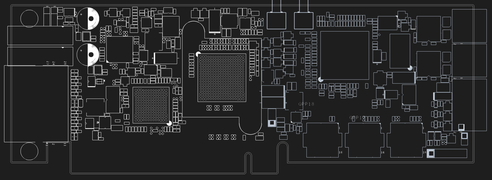
On the left side of the image is the back panel of the board - 2 USB3.0 ports are derived from it, and dual GbE ports are located under them.
I will also show our favorite technical painting with tracks on the board:
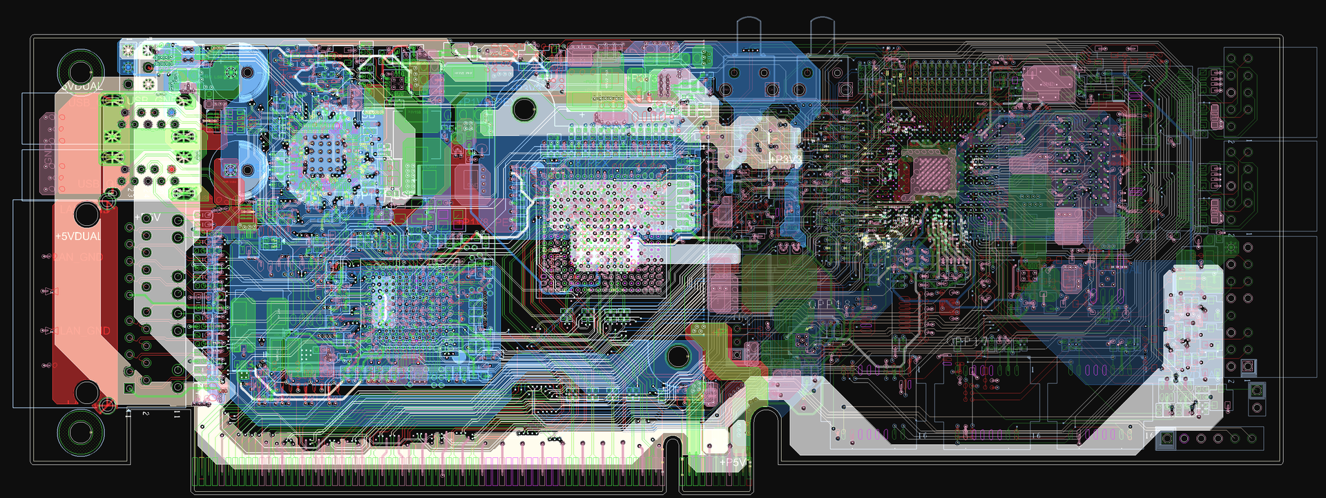
Signals and power are divided into 8 layers.
I think it’s great to print in color and hang on the wall - elegant, inspiring, and very vital! :)
Perhaps it’s worth a little more to say about BMC. We develop the firmware for it ourselves based on OpenBMC. Actually, the tasks are simple:
The resulting version, of course, in OpenBMC will commit.
Is it possible to do without this board?
Here, perhaps, the question immediately follows - but why even take out the control functions from the motherboard to a separate card? Why multiply the number of components, isn’t it easier to put everything on the motherboard, as server manufacturers usually do?
I agree that under normal conditions we would have acted just like that - but in this project and in such a matter we had to act non-standard. Due to the density of the motherboard layout, there simply wasn’t too much room to place the BMC chips, a USB host, a PCIe switch and wiring all the circuits connected with them. And besides, there was simply no place on the back of the chassis for installing Ethernet / USB connectors directly on the motherboard. In general, we decided not to complicate an already complex motherboard, and we removed all these components to a separate control board. This method, among other things, gives more flexibility in terms of future improvements and changes.
What's inside?
Actually, the structural diagram of the board is very simple:
Block diagram of the server management board.
The main component is the BMC ASPEED AST2400 chip, which is very popular and probably well known to many. It has its own dedicated 512 MB DDR3 memory.
Under the spoiler, a brief orientation about BMC, hardly interesting to experienced people in these areas.
BMC — это Baseboard Management Controller, контроллер управления системной платой. Он включается при подаче дежурного напряжения на системную плату (т.е. когда кабель подключается к блоку питания), загружает Linux из собственной ROM-памяти. В рабочем режиме мониторит работу системы — собирает информацию с датчиков (обороты вентиляторов, температуры, напряжения и токи на компонентах, датчик проникновения в корпус), считывает коды ошибок памяти, позволяет управлять компонентами системы как автоматически, так и вручную через сеть. Ведёт журналы мониторинга системы, может включать/выключать/перезагружать систему, обновлять прошивку ROM хоста, и т.д. В общем, недремлющая рабочая лошадка.
The USB3.0 host is connected to the BMC, for which we use the TI7340 chip. From it, two USB3.0 ports are output. Also, a dual-channel Gigabit Ethernet controller (BCM5720) is attached to the BMC, the ports of which are brought out. This is a very common controller that is highly supported by the POWER architecture.
The whole company is united by a PCIe switch (it was optimal to supply PEX8714 for the price), directly connected to the connector for connecting to the system board. It breeds PCIe x4 at x2 and 2 at x1.
The connector for connecting to the system board has a small feature. The connector itself is completely standard. But in order to completely eliminate the installation of the control board in a regular PCIe slot (on the motherboard we have a dedicated slot for the control board), we turned the connector 180 degrees and shifted it relative to the standard PCIe layout.
On the diagram you can also notice the VGA video output and two serial ports - they were not brought out, left in the form of header s. They are needed mainly for debugging purposes - and there is simply no space left on the external panel of the low-profile PCIe card after placing two USB and two Ethernet ports.
What does the board look like?
Actually, the geometry of the board turned out like this (the board is low-profile, but long):
On the left side of the image is the back panel of the board - 2 USB3.0 ports are derived from it, and dual GbE ports are located under them.
I will also show our favorite technical painting with tracks on the board:
Signals and power are divided into 8 layers.
I think it’s great to print in color and hang on the wall - elegant, inspiring, and very vital! :)
Perhaps it’s worth a little more to say about BMC. We develop the firmware for it ourselves based on OpenBMC. Actually, the tasks are simple:
- fix the requirements for firmware and prioritize their implementation;
- raise the original version on our server (adapting the basic functionality to our hardware);
- add the functionality we need.
The resulting version, of course, in OpenBMC will commit.