Creating an AUX input to a Kenwood GX806EF2 radio by capturing an i2c bus
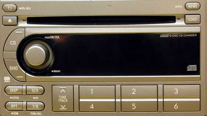
The hero of the note - the Kenwood GX806EF2 radio tape recorder - is famous for being installed in a very large number of export Japanese cars (take the Subaru Forester at least) and has neither an AUX input for connecting external audio sources, nor the ability to play MP3 files from CDs (with external drives too). The radio tape recorder came out very utilitarian for its time (2004-2007), despite the 6-CD changer. CD-audio, FM / AM tuner, and that’s all, but the cassette receiver, by the way, is gone.
But still, you can make her an AUX input without damaging the appearance and functionality.
I got this radio with a car. Having mounted the 7 "Android tablet in the navigation box, I started looking for ways to output sound from the tablet to the radio, but I didn’t want to buy a new“ head ”for this.
It turned out that many people turned off the internal CD changer and connected commercially available emulators with the ability to play MP3 via USB, for example, is like that , but it seemed like excessive vandalism to me at an extra cost.
Sound transmission from an external device can be solved using an FM transmitter, but the sound quality with this option is very poor and there are also It creates a link with extra costs for the FM transmitter and its placement in the cabin.
In some places, I found mention of cutting the AM tuner line from the radio and using its remainder for external sound, but this is not feasible with this particular radio, in all modes of the tuner, the signals go along one line. It was decided to analyze the entire circuit of the radio for “vulnerabilities”.
The glued circuit of the main board can be seen here . Here's an interesting part of the circuit: The one you are

looking for is located next to the TDA7406 audio processor (IC203 in the circuit) from STMicroelectronics. I circled in red the i2c bus, which connects the main controller to the IC203 chip, in blue - the unused MD and TAPE audio inputs. As it turns out from the datasheetto this chip, it has 4 separate stereo audio inputs and 4 separate mono audio inputs. However, not all of them are used, but unused ones are “muffled” by capacitors to the ground (C233-C236 is an example).
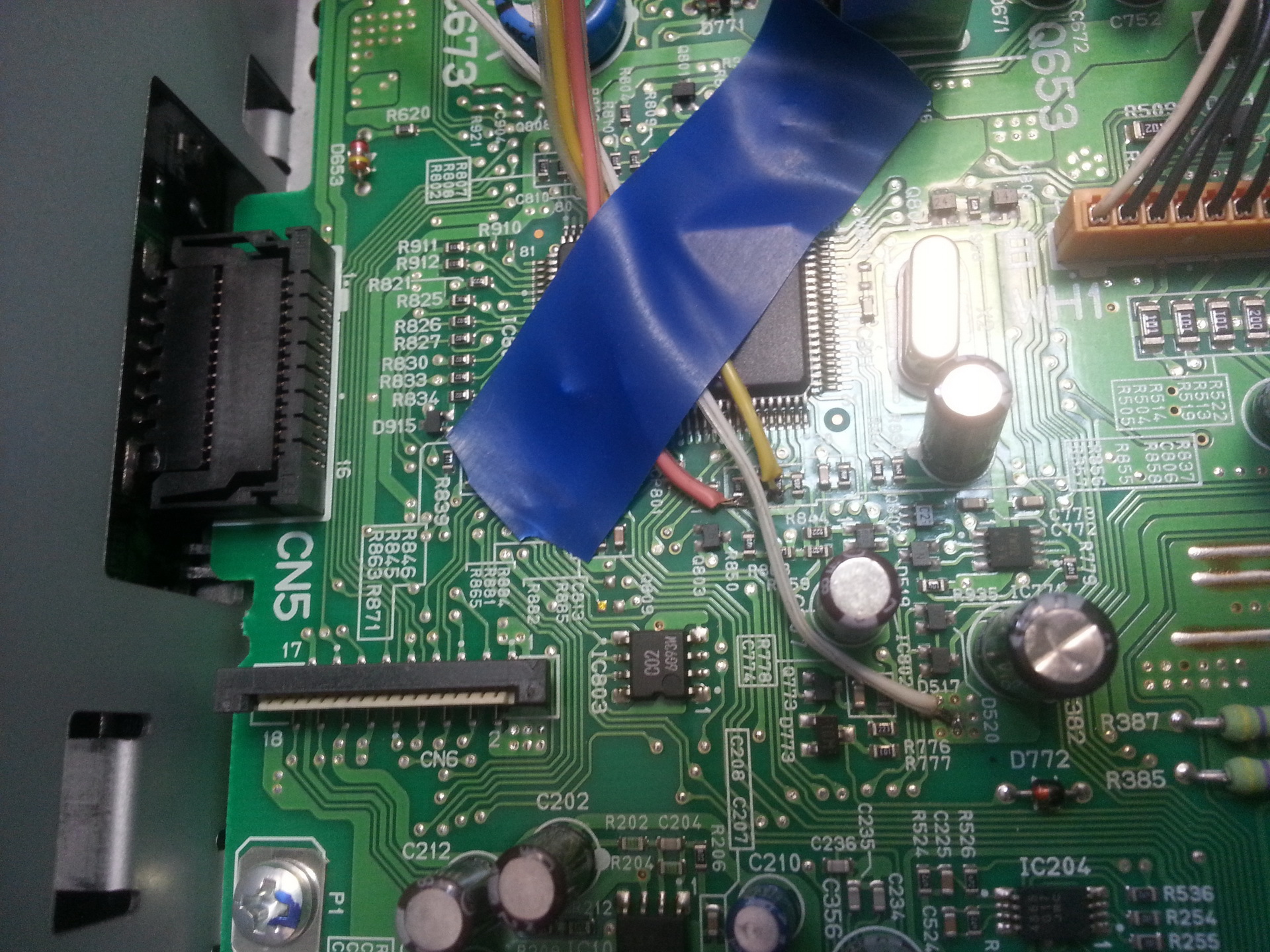
Having studied the principle of operation of the TDA7406, I realized that you can try to wedge in the control of the main controller and use unused audio inputs when necessary. I soldered the wires to the SDA and SCL lines (resistors R855, R857) and connected a logic analyzer to them:
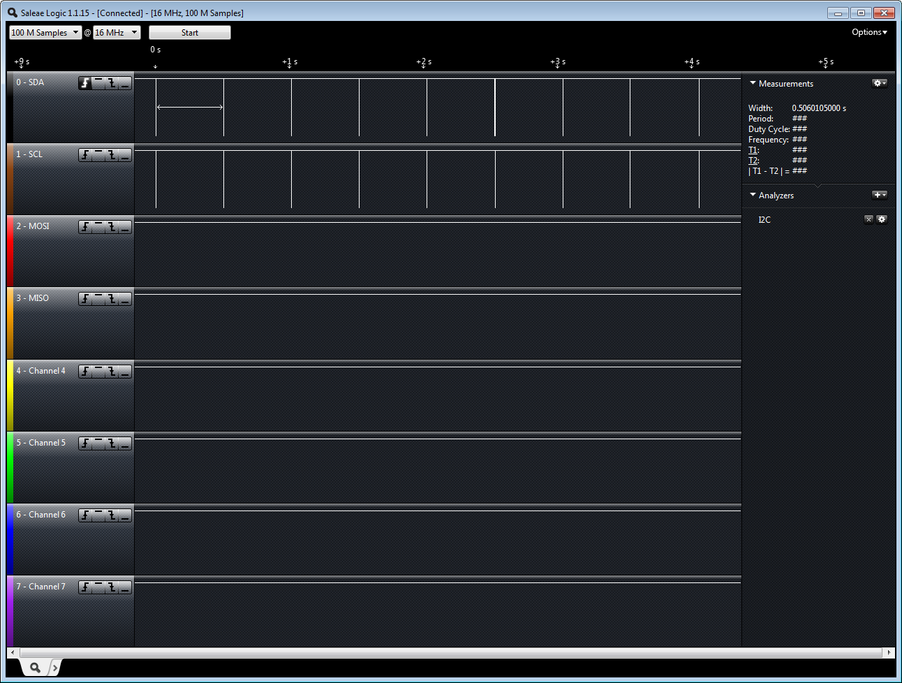
It turned out that during normal operation the controller every half second seconds requests status from TDA7406 via the i2c bus. There is nothing interesting for us in this request - there are TDA7406 status flags. There are no control commands at rest:

The most interesting thing on the bus occurs at the time of switching the CD / BAND modes and when changing the volume. In such cases, the controller provides a long message for the TDA7406 control registers. This package contains settings for almost all available registers. Here is an example of
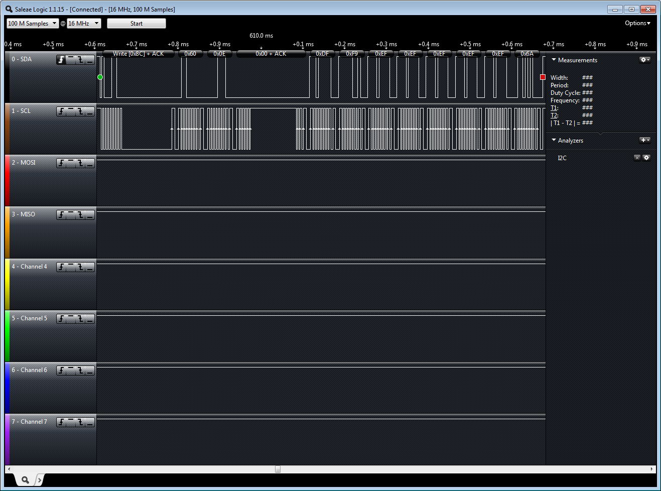
a package (its small initial part): Let's parse this package:
0x8C (chip address) - address of the TDA7406 chip with the R / W bit cleared (the controller is going to write to registers).
0x60 (subaddress) - the address of the first register from which the package will be recorded and some settings for the recording order (in this case, recording will be made from the zero address, as always when the controller configures TDA7406: it always writes the configuration starting from register 0).
0x0E (register 0) - configuration for register 0, then what we need, judging by the documentation: this is the Input Selector register. It indicates which audio mixer input should be selected now and what gain (volume) this channel should have:
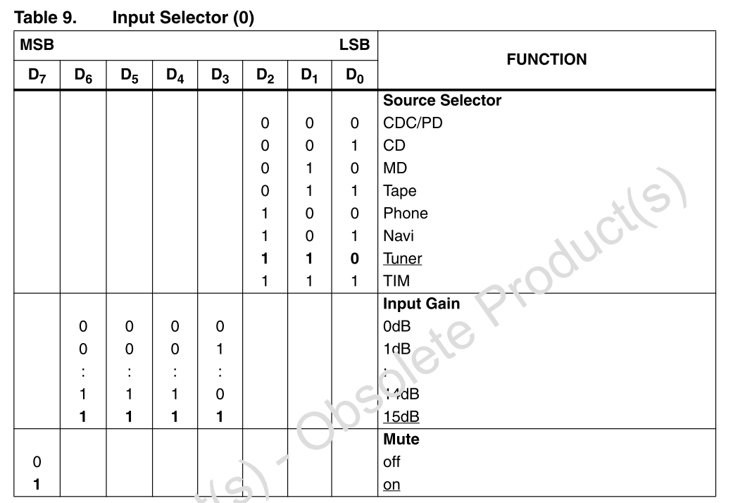
When you select a tuner channel and work with it further (increase / decrease volume), the controller sends bits 110 in the Source Selector field of the zero register. And this is very good, because in order to use the MD input for AUX, you need to transfer bits 010 to this field. For reference: the i2c bus has suspenders to the supply voltage and is always free, and the active level on the bus is zero, i.e. management is carried out by an open collector (open drain). At any time, any line of the i2c bus can be pulled to zero without damage to all devices on this bus.
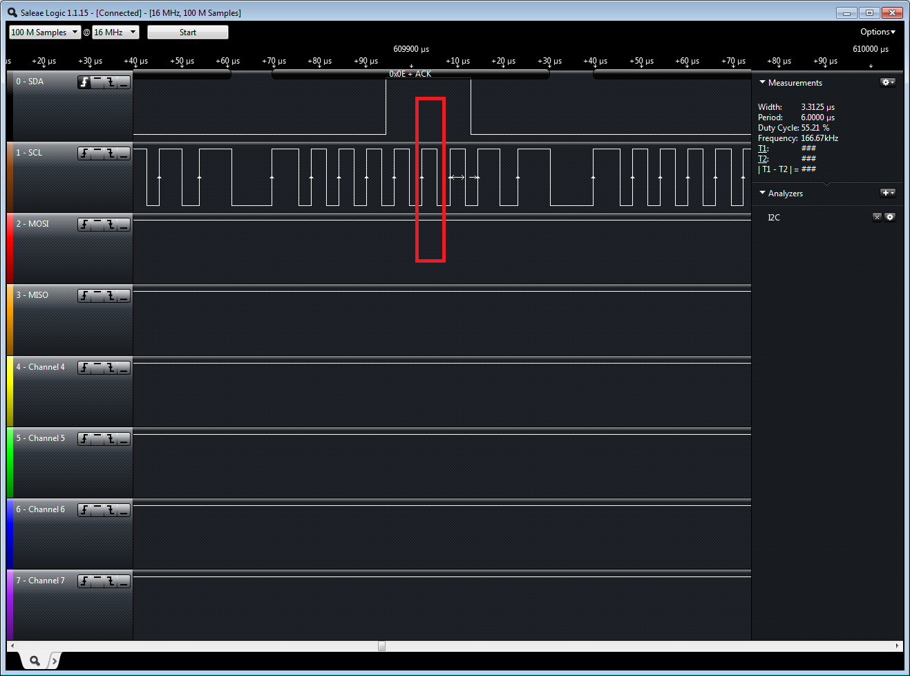
You can wedge in the controller’s communication with the audio mixer at the right time and turn the FM mode into MD mode. The only thing required is to accurately track the right time for the pulse, so that “110” turns into “010”. And you need to do this every time the controller talks to the TDA7406. Here is the moment we need on the diagram, at the time of the highlight of the SCL line in red we need to set the SDA line to zero:
I drew and made a small board with the Attiny13 microcontroller, with pin connectors on all the pins for easy programming and further connection to i2c and power:
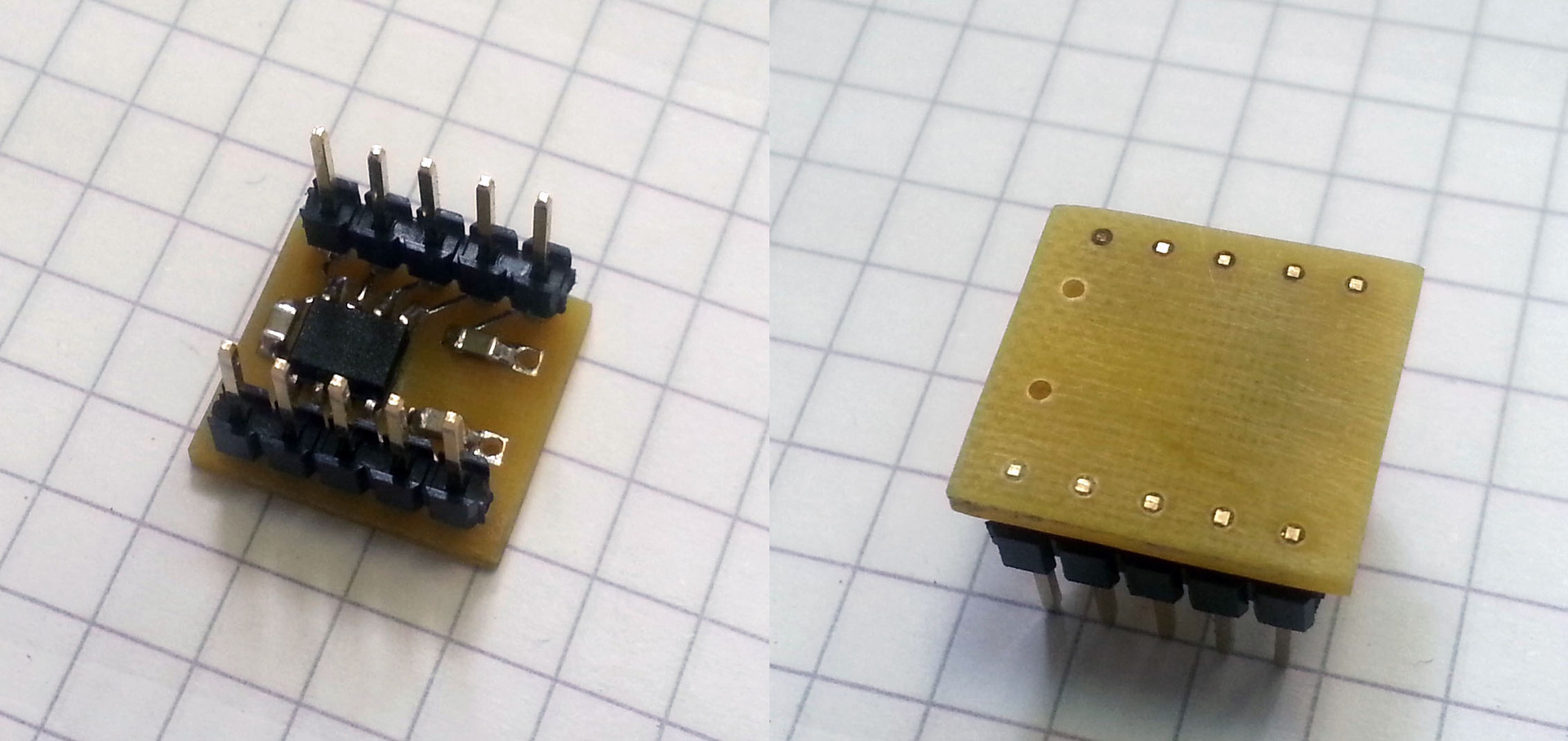
Bottom layer I deliberately made the boards flat, without sticking out the pins, so that you can easily stick the board onto the TDA7406 head.
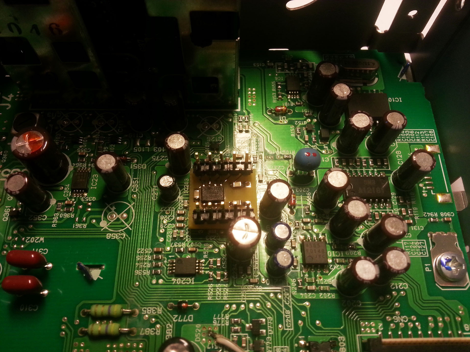
The only thing left is to solder the power wires, i2c, wires from the external 3.5 mm jack (“mother”) to the board with ATTiny13 and the wires to the radio board to the MD lines (after removing the capacitors C233, C234):

I apologize for the photo quality , was more interested in the creation process than in the documentation.
The blue wire going up in the photo goes to the News button on the front panel of the radio. It is she who is used to enable control interception audio mixer. By pressing the button we activate the interception, by another pressing - deactivate. Important: after pressing the News button, you will need to decrease or increase the volume, as at rest, as we recall, the audio mixer is not controlled, and the ATTiny13 microcontroller itself does not send any sends to the bus.
The program for the microcontroller turned out to be very simple; this is basically a solution to the “forehead” problem, without the use of interruptions. I will return to the program a little lower.
So, for those who decide to use this method to create an AUX input for this radio:
1. Disassemble the radio, remembering the types of screws and their places.
2. Get to the main board and find the TDA7406 chip.
3. Make and program the board with ATTiny13 (capacitors C1-C3 0.1 μF):
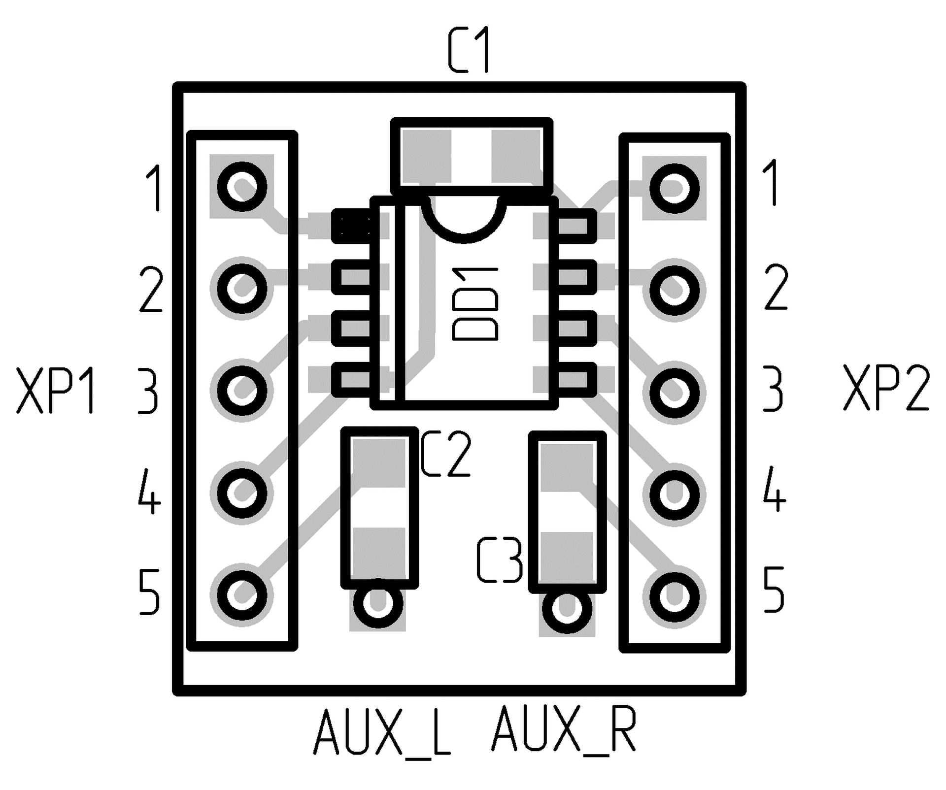
4. Glue the board to the TDA7406 chip.
5. To remove from the main board C233, C234. Solder the wiring from the main board to the ATTiny13 board according to the scheme:
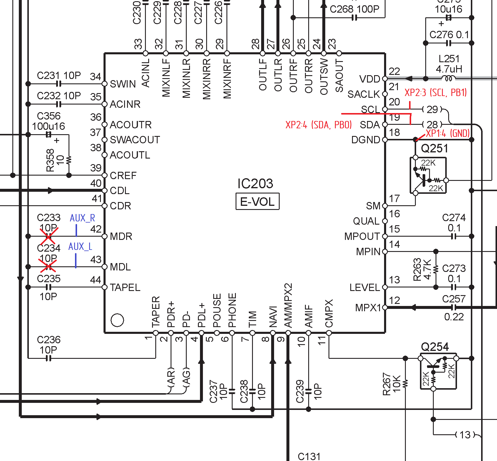
There is no power for ATTiny13 near TDA7406, as TDA7406 is powered by 8 V, and we need 5. Pull to XP2: 1 wire from pin 8 of the IC803 (24C02) memory chip, SO-8 package, see photo above.
The wire from the News button (it has two contacts, we need the one that sits on the power supply, and not on the ground) we pull to XP1: 2 (PB3).
6. Solder the AUX output itself (I have a factory 3.5mm “mother” connector with a wire from the headphone extension cord) to the board: XP1: 5 left channel, XP2: 5 right channel and common wire on XP1: 4. We start the wire from the connector before, from where it is more convenient from the outside.
7. Connect the speakers to the radio, check.
8. We solder the soldering of wires well and fix the wires to the board with elastic adhesive like “Moment”.
This modification works for me for almost a month without complaints. The only inconvenience is the two-stage on and off AUX. First, press the button News, and then straggle a little volume. This could be avoided by adding the program in such a way that ATTiny itself sent the configuration to the audio mixer registers at the moment the button was clicked, but I considered this an unnecessary intervention complicating the program. But with proper experience working with microcontrollers, this function does not last long.
A few words about the program. It does not use interrupts, and the clock (edge) tracking on the SCL line is carried out using GIFR flags in cycles. With each SCL clock, the program evaluates the status of the SDA bus and if it satisfies the sequence 0x8C 0x60 0x0E, then log.0 is set on the SDA line in the right place. And so in a circle. When using interrupts, ATTiny13 spends a lot of clocks on the input and handling of the interrupt and does not keep up with the clocks; i2c frequency is a bit high for him: 160 kHz.
The PCB P-CAD 2006 board is here .
Firmware for ATTiny13 in Intel hex format is here .
UPD: at the request of users, I add information about the "fuses."
ATTniy13 comes from production with the programmed bit CKDIV8 in Fuse Low Byte. It must be removed by writing bit 1 in its field. For example, if ATTiny13 has a Fuse Low Byte value from the factory equal to 0x6A, then it must be made equal to 0x7A. Thus, we make the maximum clock speed (9.6 MHz); at a different clock speed, the program will not work properly.