How to start developing iron using FPGAs - step by step instructions
How to increase the number of Russian engineers who would be familiar with the development of hardware, and with the development of software, and could build systems in which some of the functionality is in specialized hardware, and some in software, keeping a balance between them?
To do this, it is not at all necessary to throw out awkward money a la Skolkov's deal with MIT.
There are many cheap and effective measures to upgrade the Russian educational system. One of them is to widely introduce practical classes of FPGA / PPVM / FPGA among senior pupils and students. This is what engineers, who then develop chips inside the Apple iPhone in Cupertino, California, learn from.
FPGA - Programmable Logic Integrated Circuit
PPVM -
Field Programmable Gate Array FPGA - Field Programmable Gate Array
 Since the discussion below is about boards, many readers may immediately get the reaction “oh, it's arduino / raspberry pi / robots - we know!” No, it's not arduino, not has nothing to do with this class of devices. I repeat once again: this is not arduino, because the arduino has a microcontroller based on the microprocessor core, but there is no processor at all - a pure matrix of reprogrammable logic cells.
While American schoolchildren will play only with microcontrollers, Russian schoolchildren can play simultaneously with microcontrollers and FPGA, and thereby gain a technological advantage due to systemic thinking - understanding and programming, and the principles of developing hardware logic at the same time.
One of the problems of using FPGA for the education of Russian teenagers is the lack of literature in Russian. Pretty soon, a Russian translation of Digital Design and Computer Architecture, Second Edition, by David Harris and Sarah Harris should be published, and this problem will be partially resolved. But besides the literature describing circuitry and hardware development at the Register Transfer Level (RTL) using the Hardware Description Languages (HDL), there is another problem - for a beginner, working with student boards is not trivial, and the software environment for development - unfriendly.
Therefore, I decided to show you step by step how to start working with one of the FPGA boards, which is convenient because it sticks into a breadboard and can be used by teachers in school circles like those who started introducing circuitry through small-scale microcircuits in the 1970s. integration type K155LA3 (TTL 7400, CMOS 4000). The FPGA board plugged into the breadboard is a natural continuation of such courses.
This is how they taught the basics of digital logic from the beginning of the 1970s:
And this is what it can go to after acquainting students with the basic concepts of a logic element, trigger, and clock signal. This is the same, but on the technology of the 2010s:

The fact is that inside the FPGA there is essentially a designer of thousands of logic elements similar to elements in the K155LA3, but in the FPGA they can be connected not by hand using wires, but by changing the contents of special memory, bits that are connected to multiplexers that change the logical functions of FPGA cells and the connection between them:

Where to get boards, software for development and necessary plug-ins, I'll tell you at the end, and now dive directly in the creation of a simple circuit using a free development environment Xilinx ISE WebPACK:
input and create a new projection :

It is important to choose a folder for the project and do not mix it with your source files for the synthesizer generates all sorts of temporary files, and you can get lost in them (all of them can be removed after use):

Enter the name of the project. This name coincides with the name of the main module in Verilog (hardware description language):

Enter the FPGA parameters: Family, Device, Package, Speed. They need to be taken from the documentation on the board.

Project created:

Add source files in Verilog hardware description language.
The top.v file contains a description of the schema:
The cmods6.ucf file contains information for the development environment about how the logical inputs and outputs of the main module (btn_0, led_2, ...) are connected with the location (location, LOC) of the physical legs of the FPGA chip, which are called P8, N4, etc. . This file is a stripped-down version of the file for this board, downloaded from the Digilent website (board manufacturer):


Now click on the “generate file for FPGA programming” button. There is an important point here - “programming” - this is not software-based software programming, which boils down to creating a sequence of commands of a certain processor. The Programming File in this case is the contents of the memory in the FPGA that defines the logical functions and connections of the FPGA cells. The processor is not present in this circuit (although you can create the processor yourself by programming (in the above sense) FPGA cells).

Now press the button “look at the abstract (not tied to a specific FPGA) scheme described on the veril and synthesized by the software):


Upper module:

Click on the mouse to look inward:

Click on the“ Zoom to Full View ”button to see the whole scheme:

And now let's look at the recycled circuit generated by the software for a specific FPGA (View Technology-Specific):


We see the word LUT - this is a Look-Up Table - we need to remember it for the future:

Now click on the button “View / Edit Routed Design (FPGA Editor) “To see how the circuit will fall on the FPGA cells:


Larger:


Click the button to configure the FPGA. The board is attached with a micro-USB cable to the computer.
From now on, it’s important that the Digilent plug-in is installed for this board - digilentinc.com/Products/Detail.cfm?NavPath=2 , 66,768 & Prod = DIGILENT-PLUGIN
Digilent also has a software called Digilent Adept, but for some reason it doesn’t work on my computer with this board, so it’s better to use the plugin and iMPACT. The sequence of actions below is not necessary to understand, it’s just “magic spells” to transfer the * .bit file to the configuration memory inside the FPGA:


Everything, now the board should work - respond to button presses and blink light bulbs accordingly.
Now we will not close iMPACT, we will return to the main ISE window and build not a combinational, but a sequential circuit - a shift register. We use a 1 Hz low-frequency clock generator, i.e. once per second. The board also has an 8 MHz clock - this frequency can be increased to 200 MHz using PLL. But the high frequency is for other designs, and for clarity, 1 Hz is what you need:

Synthesize it, generate a bit-file, go back to iMPACT and press the Program button. It will say:

You need to click Yes and a new design will be loaded into the FPGA. By the way, theoretically repeated (after the creation of the iMPACT project) download should take place simply by clicking the Configure Target Device in the ISE main window, but it really doesn’t happen for me - the software tries to create a new iMPACT project. Therefore, it is better to use the Program button inside the iMPACT window. All complaints about this are in Digilent and Xilinx.
Appendix A. Two videos - how to implement a shift register and counter.
Appendix B. Full header of the top module on the veril for this board.
With all the connections and comments:
Appendix C. Where to
Get Boards Boards with Xilinx FPGAs can be found on the Digilent website, which is now a branch of National Instruments. Here is the Digilent Cmod S6 board that I used in the post with the smallest Xilinx Spartan-6 FPGA:

For further training, there are for example Nexys 4 boards with more powerful Xilinx Artix-7 FPGAs. You do not need to twist the wires on them on a breadboard, since this stage of training has already been completed:

I will write another post about boards with Altera FPGA.
Appendix D. Where to get the Xilinx ISE software
It can be downloaded directly from the Xilinx website. You can use the free version. But for Spartan-6, you need to use not the latest version of the Xilinx Vivado 2014.4 development environment, but 2013 Xilinx ISE 14.7. Why not Vivado? Marketers at Xilinx decided to switch all Spartan chip users to the newer Artix FPGAs and turned off Spartan support from the new software. Here are just boards that can be inserted into the breadboard on Artix yet. Therefore, you need to use the 2013 version of the software:

And here is the Xilinx Vivado software which supports in particular the Nexys 4 board with Xilinx Artix-7 (it is not needed for the board with Spartan-6):

Now an important point. In order to load the .bit file into the FPGA configuration memory on the board, you need to download a special plug-in from the Digilent website:


The site also has the Digilent Adept software, but I do not recommend it for Spartan-6, I had problems with it.
Appendix E. A few tags with FPGA parameters


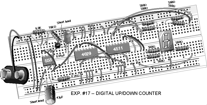
And in conclusion, another photo of the FPGA board on a breadboard with buttons, resistors and a seven-segment indicator:

To do this, it is not at all necessary to throw out awkward money a la Skolkov's deal with MIT.
There are many cheap and effective measures to upgrade the Russian educational system. One of them is to widely introduce practical classes of FPGA / PPVM / FPGA among senior pupils and students. This is what engineers, who then develop chips inside the Apple iPhone in Cupertino, California, learn from.
FPGA - Programmable Logic Integrated Circuit
PPVM -
Field Programmable Gate Array FPGA - Field Programmable Gate Array
Since the discussion below is about boards, many readers may immediately get the reaction “oh, it's arduino / raspberry pi / robots - we know!” No, it's not arduino, not has nothing to do with this class of devices. I repeat once again: this is not arduino, because the arduino has a microcontroller based on the microprocessor core, but there is no processor at all - a pure matrix of reprogrammable logic cells.While American schoolchildren will play only with microcontrollers, Russian schoolchildren can play simultaneously with microcontrollers and FPGA, and thereby gain a technological advantage due to systemic thinking - understanding and programming, and the principles of developing hardware logic at the same time.
One of the problems of using FPGA for the education of Russian teenagers is the lack of literature in Russian. Pretty soon, a Russian translation of Digital Design and Computer Architecture, Second Edition, by David Harris and Sarah Harris should be published, and this problem will be partially resolved. But besides the literature describing circuitry and hardware development at the Register Transfer Level (RTL) using the Hardware Description Languages (HDL), there is another problem - for a beginner, working with student boards is not trivial, and the software environment for development - unfriendly.
Therefore, I decided to show you step by step how to start working with one of the FPGA boards, which is convenient because it sticks into a breadboard and can be used by teachers in school circles like those who started introducing circuitry through small-scale microcircuits in the 1970s. integration type K155LA3 (TTL 7400, CMOS 4000). The FPGA board plugged into the breadboard is a natural continuation of such courses.
This is how they taught the basics of digital logic from the beginning of the 1970s:
And this is what it can go to after acquainting students with the basic concepts of a logic element, trigger, and clock signal. This is the same, but on the technology of the 2010s:
The fact is that inside the FPGA there is essentially a designer of thousands of logic elements similar to elements in the K155LA3, but in the FPGA they can be connected not by hand using wires, but by changing the contents of special memory, bits that are connected to multiplexers that change the logical functions of FPGA cells and the connection between them:
Where to get boards, software for development and necessary plug-ins, I'll tell you at the end, and now dive directly in the creation of a simple circuit using a free development environment Xilinx ISE WebPACK:
input and create a new projection :
It is important to choose a folder for the project and do not mix it with your source files for the synthesizer generates all sorts of temporary files, and you can get lost in them (all of them can be removed after use):
Enter the name of the project. This name coincides with the name of the main module in Verilog (hardware description language):
Enter the FPGA parameters: Family, Device, Package, Speed. They need to be taken from the documentation on the board.
Project created:
Add source files in Verilog hardware description language.
The top.v file contains a description of the schema:
module top
(
    input btn_0,
    input btn_1,
    output led_0,
    output led_1,
    output led_2,
    output led_3
);
    assign led_0 = btn_0;
    assign led_1 = btn_1;
    assign led_2 = btn_0 & btn_1;
    assign led_3 = btn_0 | btn_1;
endmodule
The cmods6.ucf file contains information for the development environment about how the logical inputs and outputs of the main module (btn_0, led_2, ...) are connected with the location (location, LOC) of the physical legs of the FPGA chip, which are called P8, N4, etc. . This file is a stripped-down version of the file for this board, downloaded from the Digilent website (board manufacturer):
NET "btn_0" LOC = "P8" | IOSTANDARD = LVCMOS33;
NET "btn_1" LOC = "P9" | IOSTANDARD = LVCMOS33;
NET "led_0" LOC = "N3" | IOSTANDARD = LVCMOS33;
NET "led_1" LOC = "P3" | IOSTANDARD = LVCMOS33;
NET "led_2" LOC = "N4" | IOSTANDARD = LVCMOS33;
NET "led_3" LOC = "P4" | IOSTANDARD = LVCMOS33;
Now click on the “generate file for FPGA programming” button. There is an important point here - “programming” - this is not software-based software programming, which boils down to creating a sequence of commands of a certain processor. The Programming File in this case is the contents of the memory in the FPGA that defines the logical functions and connections of the FPGA cells. The processor is not present in this circuit (although you can create the processor yourself by programming (in the above sense) FPGA cells).
Now press the button “look at the abstract (not tied to a specific FPGA) scheme described on the veril and synthesized by the software):
Upper module:
Click on the mouse to look inward:
Click on the“ Zoom to Full View ”button to see the whole scheme:
And now let's look at the recycled circuit generated by the software for a specific FPGA (View Technology-Specific):
We see the word LUT - this is a Look-Up Table - we need to remember it for the future:
Now click on the button “View / Edit Routed Design (FPGA Editor) “To see how the circuit will fall on the FPGA cells:
Larger:
Click the button to configure the FPGA. The board is attached with a micro-USB cable to the computer.
From now on, it’s important that the Digilent plug-in is installed for this board - digilentinc.com/Products/Detail.cfm?NavPath=2 , 66,768 & Prod = DIGILENT-PLUGIN
Digilent also has a software called Digilent Adept, but for some reason it doesn’t work on my computer with this board, so it’s better to use the plugin and iMPACT. The sequence of actions below is not necessary to understand, it’s just “magic spells” to transfer the * .bit file to the configuration memory inside the FPGA:
Everything, now the board should work - respond to button presses and blink light bulbs accordingly.
Now we will not close iMPACT, we will return to the main ISE window and build not a combinational, but a sequential circuit - a shift register. We use a 1 Hz low-frequency clock generator, i.e. once per second. The board also has an 8 MHz clock - this frequency can be increased to 200 MHz using PLL. But the high frequency is for other designs, and for clarity, 1 Hz is what you need:
Synthesize it, generate a bit-file, go back to iMPACT and press the Program button. It will say:
You need to click Yes and a new design will be loaded into the FPGA. By the way, theoretically repeated (after the creation of the iMPACT project) download should take place simply by clicking the Configure Target Device in the ISE main window, but it really doesn’t happen for me - the software tries to create a new iMPACT project. Therefore, it is better to use the Program button inside the iMPACT window. All complaints about this are in Digilent and Xilinx.
Appendix A. Two videos - how to implement a shift register and counter.
Appendix B. Full header of the top module on the veril for this board.
With all the connections and comments:
module cmods6
(
    input CLK, // FPGA_GCLK, 8MHz - can be raised to 200 MHz
    input CLK_LFC, // FPGA_LFC, 1 Hz
    output LED_0, // Four lights
    output LED_1,
    output LED_2,
    output LED_3,
    input BTN_0, // Two buttons
    input BTN_1,
    // DEPP interface - interface for communication with PC via USB
    input DEPP_ASTB, // Address strobe
    input DEPP_DSTB, // Data strobe
    input DEPP_WRITE, // Write enable (write operation = 0, read operation = 1)
    output DEPP_WAIT, // Ready
    inout [7: 0] DBUS,
    // General purpose I / O - a bunch of pins for bradboards
    input [7: 0] PORTA,
    input [7: 0] PORTB,
    output [6: 0] PORTC,
    input [7: 0] PORTD,
    input [7: 0] PORTE,
    output [6: 0] PORTF
);
Appendix C. Where to
Get Boards Boards with Xilinx FPGAs can be found on the Digilent website, which is now a branch of National Instruments. Here is the Digilent Cmod S6 board that I used in the post with the smallest Xilinx Spartan-6 FPGA:
For further training, there are for example Nexys 4 boards with more powerful Xilinx Artix-7 FPGAs. You do not need to twist the wires on them on a breadboard, since this stage of training has already been completed:
I will write another post about boards with Altera FPGA.
Appendix D. Where to get the Xilinx ISE software
It can be downloaded directly from the Xilinx website. You can use the free version. But for Spartan-6, you need to use not the latest version of the Xilinx Vivado 2014.4 development environment, but 2013 Xilinx ISE 14.7. Why not Vivado? Marketers at Xilinx decided to switch all Spartan chip users to the newer Artix FPGAs and turned off Spartan support from the new software. Here are just boards that can be inserted into the breadboard on Artix yet. Therefore, you need to use the 2013 version of the software:
And here is the Xilinx Vivado software which supports in particular the Nexys 4 board with Xilinx Artix-7 (it is not needed for the board with Spartan-6):
Now an important point. In order to load the .bit file into the FPGA configuration memory on the board, you need to download a special plug-in from the Digilent website:
The site also has the Digilent Adept software, but I do not recommend it for Spartan-6, I had problems with it.
Appendix E. A few tags with FPGA parameters
And in conclusion, another photo of the FPGA board on a breadboard with buttons, resistors and a seven-segment indicator: