This is Science: 3D Mass Electronic Lithography

Today you will not surprise anyone with electronic lithography; a very successful future in microelectronics is prophesied to it. Even RosNano plans to purchase Mapper electron beam lithography. And what about materials - what will become the basis of the photoresist of the future?
Ion beam lithography , in the generalized sense of the word, sooner or later has to replace traditional photolithography , as it has incomparable resolution and pattern accuracy due to the use of particles (ions or electrons) with a very short wavelength (less than 1 Angstrom or 0.1 nm). In addition, this is a method of directly creating patterns and patterns that does not require the development of expensive masks (the price of which can reach hundreds of thousands of dollars apiece), as is the case with photolithography.
For example, in the presented scheme of the photolithographic process, in the case of ion-beam lithography, we can safely exclude the mask at stage number 3:

However, in the capitalist world everything is decided by money, including the cost of equipment and raw materials - of course, photoresist, which is consumed in large volumes , since the most common chip can contain from a dozen of the most diverse layers. And in fact, it is the photoresist that is responsible for how accurately the pattern will be reproduced on the substrate.
So, a group of Chinese scientists from Canada have proposed a way to use extremely cheap polystyrene as a photoresist in electron beam lithography, allowing you to create 3D objects up to 1.5 microns high with an unusually small thickness (below a hundred nanometers).
Polydimethylsiloxane polymer ( PDMS ) is usually used in electronic lithography , but scientists have found a way to replace it with cheaper polystyrene (the market value is about 2 times lower). This increases the sensitivity, and with it the performance of the whole method as a whole, since it takes less time to create one “pixel”.
The essence of the proposed method is that polystyrene is applied to the substrate due to thermal evaporation, and then after exposure to the electron beam, the exposed area can be easily dissolved with a mixture of xylenes. As a result, a cavity forms, which can subsequently be filled with various materials: aluminum (to create contacts), silicon dioxide (to create waveguides or insulating planes) and so on.
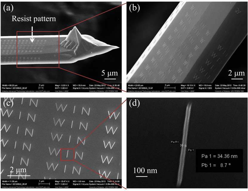
Examples of patterns obtained on polystyrene using electron beam lithography
In addition, if you wish, you can simultaneously “draw” on curved surfaces and even create waveguides on such surfaces:
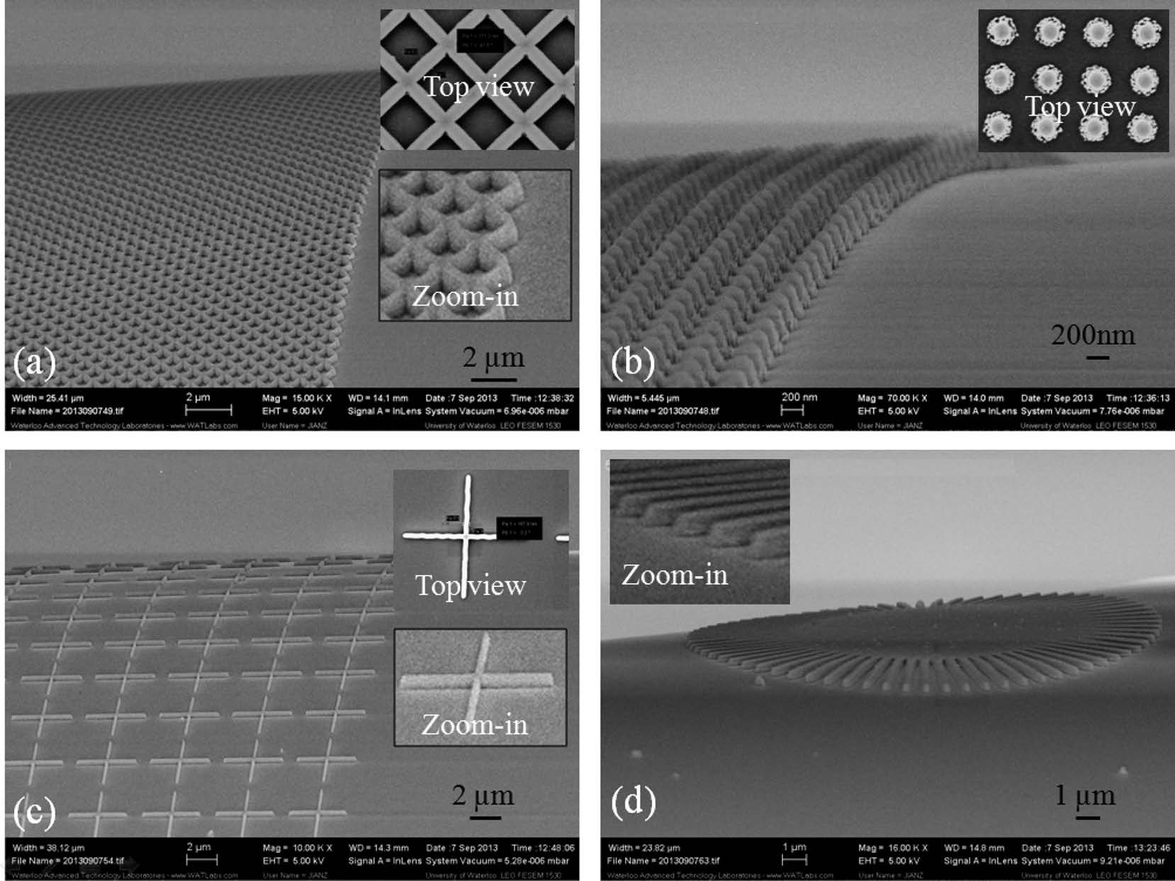
Using an electron beam, you can print on virtually any surface, creating complex patterns
Thus, the combination of properties: low cost, low dose or short exposure time, combined with the ability to create patterns on curved surfaces, actually make polystyrene in demand in the emerging market of electronic industrial lithography.
Original article in ACSNano (DOI: 10.1021 / nn4064659)
A complete list of This is Science's published articles on GeekTimes:
This is Science: Simple and Cheap Solar Energy
This is Science: Graphene - Life or Death?
This is Science: Blow and Get Electricity
This is Science: Silicon Electronics: Bend Me All the Way!
This is Science: An elastic display on quantum dots.
This is Science: Putting triboelectricity at the service of humanity.
This is Science: 3D optical printing moves to the micro level.
This is Science: What's inside a neuromorphic chip?
This is Science: News from graphene fields
This is Science: 3D electronic lithography to the masses
This is Science: Alkaline battery discharge or why the battery bounces
This is Science: micro-guns and nanocores.
This is Science: wearable electronics and triboelectricity. Part 1
This is Science: Wearable Electronics and Triboelectricity. Part 2
Sometimes it is possible to read briefly, and sometimes not so much about the news of science and technology on my Telegram channel - we are welcome;)