The probable future of microelectronics production: maskless multi-beam electron lithography from Mapper Lithography
 Someone probably already heard that at the end of 2012, Rusnano invested in the developer of electronic lithography equipment Mapper Lithography. What and how they do, whether it will save the domestic microelectronic industry - we learn in this article.
 As we recall , the production of microcircuits involves sequential processing of a semiconductor wafer through an exposed photoresist layer, the image on which is usually formed optically: a “scanner” projects an image of a photomask through a reducing lens.
This approach has a number of drawbacks: the need to produce photomasks for each new microcircuit (omit the possibility of group production here) - leads to the fact that the products must be large-scale, millions of pieces in order to cover the cost of photomasks (up to several million $ for each type of microcircuit). And on the other hand - the wavelength of light limits the minimum size of the drawn elements. Now the world industry has come close to the theoretical limit of the resolution of optical lithography: ~ 35nm for scanners NA = 1.35 with ArF lasers at a wavelength of 193nm and ~ 18nm for lithography on EUV hard ultraviolet light (however, this is not yet used in serial production).
There is an alternative: to expose the photoresist not with light, but with an electron beam - it turns out electronic lithography. The electron beam can be focused to a point of much smaller size, even 1nm is not a problem, but new problems also appear.
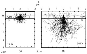
In the photo, a simulation of an electron getting into an electron resist, demonstrating the problem with the resolution of the electron resist due to electron scattering.
Limitations of Electronic Lithography
ExposureIn order to “illuminate” an electron resist, a certain number of electrons must fall on a unit area. For typical good electron-resistors, the exposure is about 30 microcoulomb per square centimeter. This means that one beam with a current of 10nA (10 nanocoulomb per second) will illuminate a 300mm plate with an area of 706 cm 2 in 706 * 30 / (10 * 0.001) = 24 days. And this despite the fact that there are several such exposures on the plate. This was one of the significant factors limiting the spread of electron lithography (such a single-beam system is no more complicated than a scanning electron microscope - and they were already sold in 1965).
Maybe you can increase the current in the beam?
Beam current
Here 2 problems appear: as we recall, the same charges repel each other. Accordingly, the electrons in flight “push” each other and make the beam wider. The greater the current (= more electrons in flight) - the stronger this effect is manifested. Accordingly, it will not work to significantly increase the current without degrading the resolution.
And finally, a beam with a relatively large current, instead of exposure to an electron resist, can fry / evaporate it (as in electron beam welding).
Electron resist
One of the remaining problems - the electrons do not just expose the electron resist when hit, but gradually lose energy, moving in its thickness randomly changing direction. It is partly possible to combat this effect by lowering the energy of electrons (= speed) - but this also forces the current to be reduced so that the electrons do not begin to “push” each other in flight. Mapper uses energy of 5 kV, respectively, the volume in which electrons are scattered is much smaller than that shown in the first photo in the article.
The principle of the multipath system
For comparison, the Mapper system is on the left, on the right is a classic single-beam electron microscope.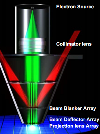
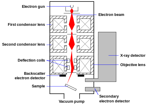
In the classical system (on the right) - the beam from the electron gun (on top) is focused by electrostatic lenses and deflected to the right place by deflecting coils or electrostatic deflectors. Directly scaling such a system would be costly - would have to duplicate all structural elements.
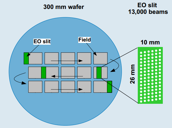
 Mapper has one powerful source of electrons, a collimator (an electrostatic lens focusing them so that a wide parallel beam of electrons is obtained). Then this wide beam hits the matrix of blankers (in the photo on the right) - actually a plate with holes, one of the walls of which has a deflecting electrode. When voltage is applied to the electrode, the electrons are deflected and go no further. If there is no current, then they will fly further in a parallel beam. In the prototype of the system, the number of rays was 7x7, now they are making a “combat” system with 13 thousand rays (in fact, there are simply more “holes” and connections to them, that's all).
 Initially (~ 2008), Mapper wanted to control these deflecting electrodes with a laser, apparently so that the conductors did not introduce distortions into the "wrong" channels.
Since even 13,000 rays are not enough to cover a strip 26 mm wide with one pass - individual deflectors go below, which can deflect each beam by about 2 micrometers along one axis (perpendicular to the movement of the plate). And finally - each beam has its own electrostatic focusing lens.
As a result, such a system is much easier to scale - all these micro-plates with “holes” are manufactured according to the already developed MEMS technological processes in serial plants, and if necessary they can be scaled further. Electronic optics is maximally simplified (= cheaper) - due to the fact that each beam must be deflected at a very small distance (2 microns), and even along one axis. Judging by the presentations, the future plans include the integration of CMOS control logic into MEMS devices, which should further expand the system's scalability.
Exposure of the entire plate is already provided by the synchronous smooth movement of the plate itself relative to the installation. This method has long been used in serial optical scanners - so here all the problems have already been solved.
Results and Summary
The Mapper prototype works, they want to achieve a resolution of 16nm (with arbitrary geometry, optical lithography on a 193nm laser in such conditions produces a minimum of 35-40nm). At the beginning of 2014, the first launches of the new system with 13 thousand rays were planned. In mass production should go in 2015-2016. However, there is a fly in the ointment: right after receiving money from Rusnano at the end of 2012, there was no more news on the company's website. I wrote to them 2 times on this subject - they are silent like a fish on ice.When investing, RUSNANO ordered the company to transfer part of the production to the Russian Federation, and it was planned to transfer micro-optics precisely. This is done or not at the moment - it is not known, on the Rusnano website it is written that something is happening in the technopolis “Moscow” .
By the cost of the final apparatus, the manufacturer is guided by the cost comparable with EUV scanners based on 1 plate per hour (~ 500 thousand $ / wph). Because Mapper maximum productivity in one installation turns out 10 plates per hour, to get the same ~ 100 plates per hour - it is proposed to install the system in several copies.
When the system goes into mass production, we can expect a further decrease in cost, because there are no painful places in optical photolithography — a light source (both EUV and ArF lasers cost a lot of money), a complex and monstrously expensive lens, and photo templates that need to be manufactured for each new type of manufactured microcircuit. And electronic microoptics - is mass-produced at least in a million copies without any problems.
The emergence of such systems - also promises to reduce the cost of small-scale microcircuits, there will be an alternative to FPGA with much greater performance.
The military especially likes these systems and fits perfectly into the current Russian concept of “small dual-use microelectronic production”. However, it is too early to rejoice - RUSNANO is only one of the investors and the manufacturer will in any case be forced to comply with the export control requirements of all countries involved in the development. And this means that it will be possible to get such a system in Russia only for civil proceedings, and it is with them (or rather, their absence) that we have a problem - I will write more about this in more detail.
Links
2008: MAPPER: High Throughput Maskless Lithography
2010:MAPPER: High Throughput Maskless lithography
2010, SPIE: MAPPER: High Throughput Maskless lithography
2012: RUSNANO invests in maskless lithography with a resolution of up to 10 nm
2013: Lithography Cost-Effective Solutions for 1X nodes