New technological processes for the production of microchips are increasingly being put off - why?
At the end of August, GlobalFoundries, a semiconductor integrated circuit manufacturer (working with AMD), stopped developing 7-nanometer manufacturing processes. A few months earlier, Intel announced that it was again delaying the release of its 10-nanometer chip.
We explain further the reasons for these decisions and the situation in the industry.
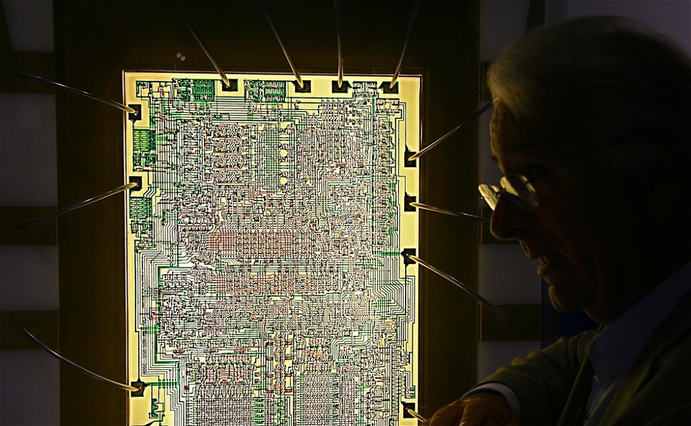
/ photo Intel Free Press CC
Separate transistors on a chip are formed by photolithography . In this case, a thin photosensitive polymer film called a photoresist is applied to the silicon substrate. Then this photo layer is treated with light (the so-called exposure is made) through a photo template with the necessary pattern. Exposed areas are washed off in the developer, and then the crystals are etched.
Companies are reducing technological processes to increase the number of products from one workpiece and reduce the energy consumption of the final chip. The manufacturer gets the opportunity to increase the speed of the chip, leaving its dimensions unchanged.
For a long time, this tendency (to reduce technological processes) remained fair. But now, IT companies have begun to delay or even stop developing new technological processes. This is partly due to the rise in price of equipment and a high level of marriage.
More details on the situation are discussed below.
GlobalFoundries produce silicon wafers at eight plants around the world. The company was supposed to launch a 7-nm chip in the second quarter of 2018. However, a couple of weeks before the expected release, GlobalFoundries decided to cancel everything.
Instead, the organization will focus on developing specialized production standards for 14LPP (Low-Power Plus) and 12LP (Leading-Performance) and creating various built-in storage devices .
The 14LPP platform is an improved version of the 14nm process based on the 3D FinFET transistor. It increases the performance of devices by 55% and reduces their power consumption by 60% (compared to 28 nm). A 12LP- This is a manufacturing process for semiconductors, sharpened for the needs of AI systems, smartphones and automotive electronics.
According to CTO GlobalFoundries Gary Patton, the reason for the strategic turn was not technical problems, but financial issues. The company has invested billions of dollars in the development of 7-nanometer chips. The first generation, which uses immersion lithography, was almost completed. But the second and third (they required deeper UV ranges to increase the density of transistors) did not have enough funds.
Together with the cancellation of 7-nm, GlobalFoundries stopped the development of 5-nanometer and 3-nanometer manufacturing processes. Due to the change of course, GlobalFoundries will cut five percent of its employees and review agreements with AMD and IBM. In particular, the company will work with IBM until the end of the year, and then stop researching new technological processes.
Another organization that delayed the release of chips on a new process was Intel. The IT giant has been moving the massive release of 10nm circuits for two years now. This time, the start of sales of the first 10-nm products was moved to the end of 2019.
According to company representatives , the reason for the delay is the low yield of suitable processors. It is believed that the problem is associated with multi-patterning technology and the use of cobalt.
Production volumes are growing slower than planned. Technically, Intel is already supplying 10nm chips in small batches. For example, the first Core i3-8121U - 10 nm processors of the Cannon Lake family - are already workingon Lenovo laptops. However, there is no need to talk about the mass production of chips.
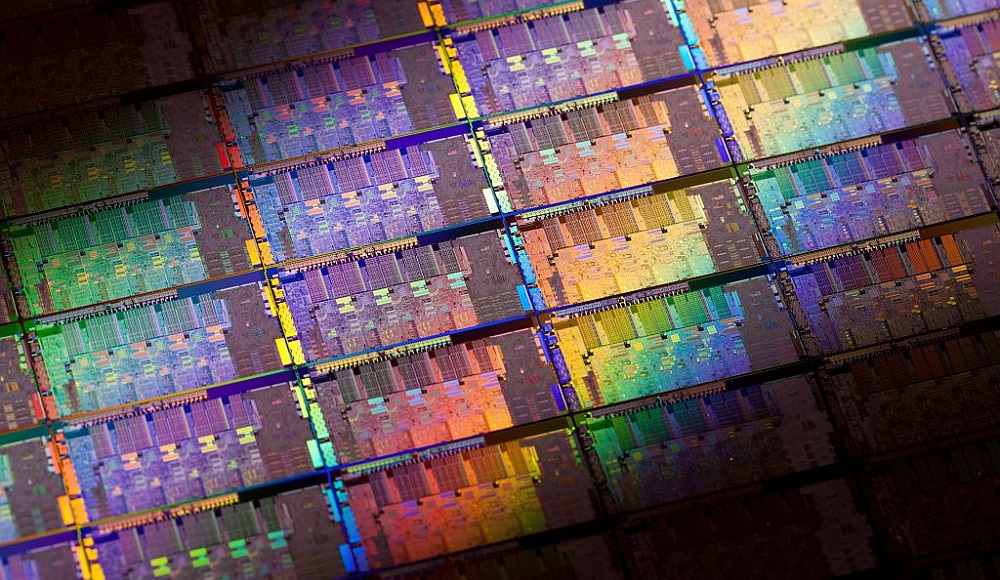
/ photo Intel Free Press CC
Other market players are also in no hurry to put the development of new technological processes on stream. UMC has so far settled on a 14-nm process technology, while Samsung has promised 7-nm, but also not earlier than 2019.
As we have already said, the high cost of transition is one of the reasons why GlobalFoundries curtailed their projects. And according to Gartner, she is the main one. According to analysts, the cost of developing 7-nm technology is approximately $ 270 million.
Equipment for EUV lithography , nanosheets, exotic materials like ruthenium - all these things are not cheap, but some of them are already difficult to do. To recoup the investment in production, it is necessary to produce 150 million chips per year. Therefore, the implementation of 7-, 5-, 3- and 2-nm processes may be commercially disadvantageous.
Moreover, even if they create a microcircuit, the “exhaust” in performance does not always turn out to be significant. For example, Qualcomm believesthat the 5-nm process will not greatly exceed the 7-nm in characteristics, and it will take several billion dollars to invest in its development.
The second reason is the high probability of error and its price. For example, delays in the supply of 10-nm Intel process technology " flew a pretty penny " to one of the IT giants with a capitalization of $ 20 billion.
HN residents highlight other reasons for the slowdown in the semiconductor industry. For example, one of the users believes that reducing the size of the crystal has a bad effect on its cooling. Therefore, companies are trying to invest in the development of more energy-efficient technologies, rather than reducing the size of the crystals (this is the path that GlobalFoundries has chosen).
Industry representatives believe that technological processes will still have to be reduced. This will ensure the effective operation of AI, MO, 5G networks and IoT. According to preliminary calculations by developers from TSMC, the 7-nm process technology will improve productivity by 30% and half reduce the power consumption of the processor (compared to 10-nm).
However, David Hemker, senior VP at Lam Research, a semiconductor manufacturing company, stresses that the industry will need new solutions to cope with the growing complexity of manufacturing processes.
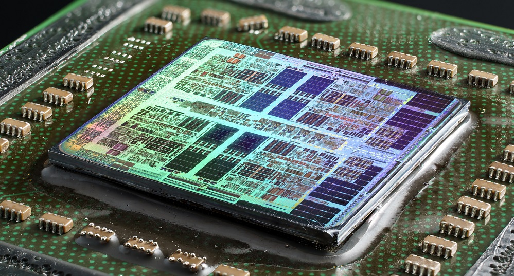
/ photo Fritzchens Fritz PD
So far, EUV lithography generates too many defects in chip manufacturing. But if we continue to improve the technology, it should reduce the time and costs of developing new technological processes.
Despite all the difficulties of production, some industry representatives already make forecasts for processes less than 5 nm and talk about the timing of the release of such chips. So, for example, TSMC - also engaged in the production of semiconductors - is already making plans to develop 3- and 2-nm process technology. And the Imec research center, together with Cadence Design Systems, even developed test samples of microprocessors using 3-nm technology.
Therefore, in the future we will definitely see the application of these technologies, only this moment can come a little later than originally assumed.
PS Additional Resources from the First Corporate IaaS Blog:
PPS Related articles from our blog on Habré:
What we do in IT-GRAD: • IaaS • PCI DSS hosting • Cloud ФЗ-152
We explain further the reasons for these decisions and the situation in the industry.
/ photo Intel Free Press CC
A few words about technological processes
Separate transistors on a chip are formed by photolithography . In this case, a thin photosensitive polymer film called a photoresist is applied to the silicon substrate. Then this photo layer is treated with light (the so-called exposure is made) through a photo template with the necessary pattern. Exposed areas are washed off in the developer, and then the crystals are etched.
Companies are reducing technological processes to increase the number of products from one workpiece and reduce the energy consumption of the final chip. The manufacturer gets the opportunity to increase the speed of the chip, leaving its dimensions unchanged.
For a long time, this tendency (to reduce technological processes) remained fair. But now, IT companies have begun to delay or even stop developing new technological processes. This is partly due to the rise in price of equipment and a high level of marriage.
More details on the situation are discussed below.
Why GlobalFoundries Canceled 7nm
GlobalFoundries produce silicon wafers at eight plants around the world. The company was supposed to launch a 7-nm chip in the second quarter of 2018. However, a couple of weeks before the expected release, GlobalFoundries decided to cancel everything.
Instead, the organization will focus on developing specialized production standards for 14LPP (Low-Power Plus) and 12LP (Leading-Performance) and creating various built-in storage devices .
The 14LPP platform is an improved version of the 14nm process based on the 3D FinFET transistor. It increases the performance of devices by 55% and reduces their power consumption by 60% (compared to 28 nm). A 12LP- This is a manufacturing process for semiconductors, sharpened for the needs of AI systems, smartphones and automotive electronics.
According to CTO GlobalFoundries Gary Patton, the reason for the strategic turn was not technical problems, but financial issues. The company has invested billions of dollars in the development of 7-nanometer chips. The first generation, which uses immersion lithography, was almost completed. But the second and third (they required deeper UV ranges to increase the density of transistors) did not have enough funds.
Together with the cancellation of 7-nm, GlobalFoundries stopped the development of 5-nanometer and 3-nanometer manufacturing processes. Due to the change of course, GlobalFoundries will cut five percent of its employees and review agreements with AMD and IBM. In particular, the company will work with IBM until the end of the year, and then stop researching new technological processes.
Who else postponed development
Another organization that delayed the release of chips on a new process was Intel. The IT giant has been moving the massive release of 10nm circuits for two years now. This time, the start of sales of the first 10-nm products was moved to the end of 2019.
According to company representatives , the reason for the delay is the low yield of suitable processors. It is believed that the problem is associated with multi-patterning technology and the use of cobalt.
Production volumes are growing slower than planned. Technically, Intel is already supplying 10nm chips in small batches. For example, the first Core i3-8121U - 10 nm processors of the Cannon Lake family - are already workingon Lenovo laptops. However, there is no need to talk about the mass production of chips.
/ photo Intel Free Press CC
Other market players are also in no hurry to put the development of new technological processes on stream. UMC has so far settled on a 14-nm process technology, while Samsung has promised 7-nm, but also not earlier than 2019.
Main reasons
As we have already said, the high cost of transition is one of the reasons why GlobalFoundries curtailed their projects. And according to Gartner, she is the main one. According to analysts, the cost of developing 7-nm technology is approximately $ 270 million.
Equipment for EUV lithography , nanosheets, exotic materials like ruthenium - all these things are not cheap, but some of them are already difficult to do. To recoup the investment in production, it is necessary to produce 150 million chips per year. Therefore, the implementation of 7-, 5-, 3- and 2-nm processes may be commercially disadvantageous.
Moreover, even if they create a microcircuit, the “exhaust” in performance does not always turn out to be significant. For example, Qualcomm believesthat the 5-nm process will not greatly exceed the 7-nm in characteristics, and it will take several billion dollars to invest in its development.
The second reason is the high probability of error and its price. For example, delays in the supply of 10-nm Intel process technology " flew a pretty penny " to one of the IT giants with a capitalization of $ 20 billion.
HN residents highlight other reasons for the slowdown in the semiconductor industry. For example, one of the users believes that reducing the size of the crystal has a bad effect on its cooling. Therefore, companies are trying to invest in the development of more energy-efficient technologies, rather than reducing the size of the crystals (this is the path that GlobalFoundries has chosen).
Why updates are still needed
Industry representatives believe that technological processes will still have to be reduced. This will ensure the effective operation of AI, MO, 5G networks and IoT. According to preliminary calculations by developers from TSMC, the 7-nm process technology will improve productivity by 30% and half reduce the power consumption of the processor (compared to 10-nm).
However, David Hemker, senior VP at Lam Research, a semiconductor manufacturing company, stresses that the industry will need new solutions to cope with the growing complexity of manufacturing processes.
/ photo Fritzchens Fritz PD
So far, EUV lithography generates too many defects in chip manufacturing. But if we continue to improve the technology, it should reduce the time and costs of developing new technological processes.
Despite all the difficulties of production, some industry representatives already make forecasts for processes less than 5 nm and talk about the timing of the release of such chips. So, for example, TSMC - also engaged in the production of semiconductors - is already making plans to develop 3- and 2-nm process technology. And the Imec research center, together with Cadence Design Systems, even developed test samples of microprocessors using 3-nm technology.
Therefore, in the future we will definitely see the application of these technologies, only this moment can come a little later than originally assumed.
PS Additional Resources from the First Corporate IaaS Blog:
- New functionality in VMware vSphere 6.7
- Examples of NetApp Storage Applications in Various Business Areas
- Cloud Disk Testing
PPS Related articles from our blog on Habré:
- The Japanese introduced a prototype processor for exaflops supercomputer
- IBM introduced the world's first 5-nanometer chip
- Why computer chips have become faster "aging" and what to do about it
What we do in IT-GRAD: • IaaS • PCI DSS hosting • Cloud ФЗ-152