Description of memory blocks in VHDL
- From the sandbox
- Tutorial
This article shows the basic principles for describing the ROM and RAM modules in VHDL. This article is for beginners. Its purpose is to give a general concept about the description of memory modules in the VHDL language. Examples and illustrations are provided for Quartus II v. 9.1. It is assumed that the reader knows how to create a project in the Quartus II package, to compile and simulate it.
VHDL memory is described as an array of (
For example, for a memory module of 32 cells, each of which contains 8 bits, it is necessary to declare an array containing 32 vectors, each of which is eight-bit.
Next, it is necessary to describe the address inputs, data inputs and outputs, control signals. The type of data ports must match the data type of a single cell. For the above example, this is
The data type for the address —
The description of the memory is best done by parameterizing the modules. This permits reuse of the written code. The following is an example of a 32 × 8 parameterized module. In the example, to describe the memory module, the
When describing read-only memory devices, the contents of the cells must be determined when writing the program. You can use several options for determining the contents of memory:
Of the three options, the first two can be implemented on FPGAs of any manufacturer, and the third is possible only in the Quartus II package.
When using this option, you must first declare a type that will match the size of the memory block. Then a constant of this type is declared and the contents of all the cells of the array are determined.
For example, declare a new type of ROM, which is an array with 8 cells, each of which has a size of 8 bits. Then we define a Content constant of type ROM.
To use such a constant, you just need to address the required cell in the array using input from address lines. The source data port must be of the same type as the cell type of the memory block. For the above example, the source port
Example 1. Consider an example of a complete description of a memory block using a constant. The memory block that meets this description is shown in Figure 1.

Figure 1 - The memory block described in Example 1
Lines 13 and 14 declare an array type of 32 cells, each of which contains 8 bits.
Lines 15 through 23 specify the value of the cells in the array. Separately, the values are determined only for the first 16 cells - lines 16 to 22. All other cells are filled with the same value "1111 1111" using the word others - line 23. The
operation of the memory module is described using the process operator, the initialization list of which includes signals
Line 29 checks for the leading edge of the clock signal
Lines 30-35 describe the process of reading information from ROM. If the signal
The simulation results are shown in Figure 2.
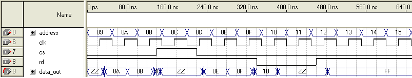
Figure 2 - The results of the simulation of the memory block
Determining the contents of memory using an operator
When using the case operator, it is necessary to declare ports, and the determination of the contents of memory occurs in the architectural body. Each address value corresponds to the contents of this memory cell. The design will look like this:
Example 2. As an example, consider the description of a 256 × 6 memory module. The address is described by an eight-bit type vector
The simulation results of the memory block from example 2 are shown in Figure 3.
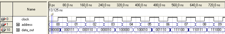
Figure 3 - Modeling the memory block from example 2
This option to determine the contents of memory only works with Altera products, but it also allows you to change the contents of memory very quickly. To describe, you must connect the Altera synthesis attribute library
To use this attribute, you must declare the synthesis attribute as a string type:
Create an attribute link
Example 3. The example describes the description of a 256 × 8 memory block. Lines 1-4 describe the libraries and modules of these libraries. It can be seen that lines 1 and 4 describe the library of synthesis attributes.
Lines 5-9 describe the interface part of the module.
Lines 11 and 12 introduce the type
In line 13, an attribute of
The use of the memory module is described in line 19 and represents only the output to the source port of the contents of the cell, which is determined by the address signal.
The contents of the mif file is determined using the mif file editor. For the given example, the window with the contents of the memory is shown in Figure 4, and the modulation results are shown in Figure 5.
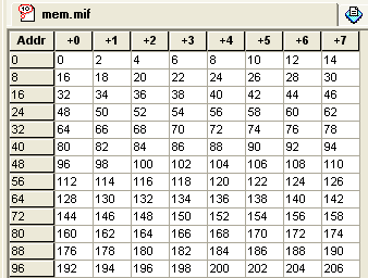
Figure 4 - The contents of the memory module
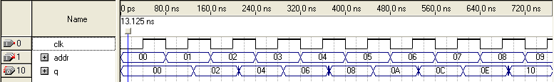
Figure 5 - Timing diagrams of the memory module from Example 3
The description of random access memory (RAM) differs from the description of read-only memory in that it is possible to record in RAM.
As an example, consider synchronous RAM. His work is described in the following table:
As in the previous examples for working with memory, we define a new type as an array, which has the dimensions of the necessary memory module.
The results of the stimulator operation of the memory module are shown in Figure 6. Here it is necessary to pay attention to the fact that the initial content of all memory cells is zero. This is visible when reading cells with numbers 6-8.
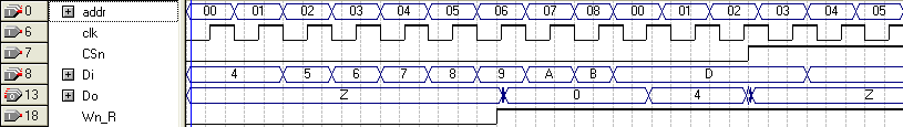
Figure 6 - Timing diagrams of RAM in
more detail in Quartus II Hahdbook any version. For example, the current one is 13 . Section 6 - Recommended HDL Coding Style.
General Provisions
VHDL memory is described as an array of (
array) vectors. The bit depth of a vector is determined by the width of the memory cell, and the number of vectors is determined by the number of cells in the memory module. For example, for a memory module of 32 cells, each of which contains 8 bits, it is necessary to declare an array containing 32 vectors, each of which is eight-bit.
type mem is array (0 to 31) of std_logic_vector (7 downto 0);
Next, it is necessary to describe the address inputs, data inputs and outputs, control signals. The type of data ports must match the data type of a single cell. For the above example, this is
std_logic_vector (7 downto 0).data_in: in std_logic_vector (7 downto 0);
data_out: out std_logic_vector (7 downto 0);
The data type for the address —
integer or types based on it. The type is integer necessary because the address is used as the index of the memory array.addr: in integer range 0 to 31;
The description of the memory is best done by parameterizing the modules. This permits reuse of the written code. The following is an example of a 32 × 8 parameterized module. In the example, to describe the memory module, the
addr_widthand parameters are used data_width, which specify the width of the address and data buses, respectively. The number of cells in the memory block in this case is determined as 2**addr_width, and their capacity is equal data_width.generic (addr_width: natural:= 5;
data_width: natural:=8);
port (
addr: in integer range 0 to 2**addr_width - 1;
data_in: in std_logic_vector (data_width-1 downto 0);
data_out: out std_logic_vector (data_width-1 downto 0)
);
type mem is array (2**addr_width-1 downto 0) of std_logic_vector (7 downto 0);
Description of read-only memory devices in VHDL language
When describing read-only memory devices, the contents of the cells must be determined when writing the program. You can use several options for determining the contents of memory:
- creation of a constant or signal of the "array" type;
- operator use
case; - use of * .mif file and synthesis attributes.
Of the three options, the first two can be implemented on FPGAs of any manufacturer, and the third is possible only in the Quartus II package.
Determining the contents of memory using a constant or an array.
When using this option, you must first declare a type that will match the size of the memory block. Then a constant of this type is declared and the contents of all the cells of the array are determined.
For example, declare a new type of ROM, which is an array with 8 cells, each of which has a size of 8 bits. Then we define a Content constant of type ROM.
type ROM is array (0 to 7) of  std_logic_vector
(7 downto 0);
constant Content: ROM := (
    0 => "00000001",
    1 => "00000010",
    2 => "00000011",
    3 => "00000100",
    4 => "00000101",
    5 => "00000110",
    6 => "00000111",
    7 => "00001000",
);
To use such a constant, you just need to address the required cell in the array using input from address lines. The source data port must be of the same type as the cell type of the memory block. For the above example, the source port
Data_out must be of type std_logic_vector (7 downto 0). Access to the contents of the memory will look like this:Data_out <= Content (Addr);
Example 1. Consider an example of a complete description of a memory block using a constant. The memory block that meets this description is shown in Figure 1.
Figure 1 - The memory block described in Example 1
Lines 13 and 14 declare an array type of 32 cells, each of which contains 8 bits.
Lines 15 through 23 specify the value of the cells in the array. Separately, the values are determined only for the first 16 cells - lines 16 to 22. All other cells are filled with the same value "1111 1111" using the word others - line 23. The
operation of the memory module is described using the process operator, the initialization list of which includes signals
clk, cs - clock and crystal selection, respectively. If the signalcs equals one, the initial ROM lines go into the Z-state (lines 27 and 28). If the signal cs is equal to zero, then the outputs go to the working state and the microcircuit works. Line 29 checks for the leading edge of the clock signal
clk. Lines 30-35 describe the process of reading information from ROM. If the signal
rd is equal to one, then information is allowed to read, if it is equal to zero, the initial lines go into the Z-state (line 32). To access a specific cell in the memory module, line 30 is used. The constant constant has the data type of the cell std_logic_vector, which corresponds to the type of the original signal data_out. The address signal in the memory module is also of type std_logic_vector, therefore, for addressing a cell in the content array, the necessary type conversionstd_logic_vectorto the type integerthat is performed using the construct to_integer (unsigned (address). In this design, the type signal is first std_logic_vectorconverted to the type signal unsigned, and only then to the type integer. More clearly about type conversion here .1 library ieee;
2 use ieee.std_logic_1164.all;
3 use ieee.numeric_std.all;
4 entity ROM is
5 port (clk : in std_logic;
6 cs : in std_logic;
7 rd : in std_logic;
8 address : in std_logic_vector(4 downto 0);
9 data_out: out std_logic_vector(7 downto 0));
10 end ROM;
11 architecture behav of ROM is
12 type ROM_array is array (0 to 31)
13 of std_logic_vector(7 downto 0);
14 constant content: ROM_array := (
15 0 => "00000001",
16 1 => "00000010",
17 2 => "00000011",
18 . . .
19 12 => "00001101",
20 13 => "00001110",
21 14 => "00001111",
22 others => "11111111");
23 begin
24 process(clk, cs)
25 begin
26 if(cs = '1' ) then
27 data_out <= "ZZZZZZZZ";
28 elsif (clk'event and clk = '1') then
29 if rd = '1' then
30 data_out <= content(to_integer (unsigned (address)));
31 else
32 data_out <= "ZZZZZZZZ";
33 end if;
34 end if;
35 end process;
36 end behav;
The simulation results are shown in Figure 2.
Figure 2 - The results of the simulation of the memory block
Determining the contents of memory using an operator case.
When using the case operator, it is necessary to declare ports, and the determination of the contents of memory occurs in the architectural body. Each address value corresponds to the contents of this memory cell. The design will look like this:
when адрес => исходный_порт <= содержимое_ячейки;
Example 2. As an example, consider the description of a 256 × 6 memory module. The address is described by an eight-bit type vector
std_logic, the data output is described by a six-bit type vector std_logic. Using the case operator, the contents of the first ten cells of the memory block are separately determined, all others are determined together with the help of operators when others.library ieee;
use ieee.std_logic_1164.all;
entity mem is
port (
clock : in std_logic;
address : in std_logic_vector (7 downto 0);
data_out : out std_logic_vector (5 downto 0));
end mem;
architecture rtl of mem is
begin
process (clock)
begin
if rising_edge (clock) then
case address is
when "00000000" => data_out <= "000111";
when "00000001" => data_out <= "000110";
when "00000010" => data_out <= "000010";
when "00000011" => data_out <= "100000";
when "00000100" => data_out <= "100010";
when "00000101" => data_out <= "001110";
when "00000110" => data_out <= "111100";
when "00000111" => data_out <= "110111";
when "00001000" => data_out <= "111000";
when "00001001" => data_out <= "100110";
when others => data_out <= "101111";
end case;
end if;
end process;
end rtl;
The simulation results of the memory block from example 2 are shown in Figure 3.
Figure 3 - Modeling the memory block from example 2
Determining the contents of memory using an mif file.
This option to determine the contents of memory only works with Altera products, but it also allows you to change the contents of memory very quickly. To describe, you must connect the Altera synthesis attribute library
altera_syn_attributesand use the attribute ram_init_file. By default, the library is in the folder папка_quartus\libraries\vhdl\altera. This attribute specifies an mif file that contains information about the contents of memory. To use this attribute, you must declare the synthesis attribute as a string type:
attribute ram_init_file : string;
Create an attribute link
ram_init_filewith the signal that describes the memory block. The attribute value must match the name of the * .mif file:attribute ram_init_file of rom : signal is "mem.mif";
Example 3. The example describes the description of a 256 × 8 memory block. Lines 1-4 describe the libraries and modules of these libraries. It can be seen that lines 1 and 4 describe the library of synthesis attributes.
Lines 5-9 describe the interface part of the module.
Lines 11 and 12 introduce the type
mem_tand signal of rom this type, which describe the memory module. In line 13, an attribute of
ram_init_filetype string is set, and in line 14, this attribute associates with the signal romand a link is made to the mem.mif file, in which the contents of the memory module are listed. The use of the memory module is described in line 19 and represents only the output to the source port of the contents of the cell, which is determined by the address signal.
1	library ieee, altera;
2	use ieee.std_logic_1164.all;
3	use ieee.numeric_std.all;
4	use altera.altera_syn_attributes.all;
5	entity mem is
6		port (clk: in std_logic;
7			  addr: in natural range 0 to 255;
8			q: out std_logic_vector (7 downto 0));
9	end entity;
10	architecture rtl of mem is
11		type mem_t is array (255 downto 0) of std_logic_vector(7 downto 0);
12		signal rom: mem_t;
13		attribute ram_init_file: string;
14		attribute ram_init_file of rom: signal is "mem.mif";
15	begin
16		process(clk)
17		begin
18		if(rising_edge(clk)) then
19			q <= rom(addr);
20		end if;
21		end process;
22	end rtl;
The contents of the mif file is determined using the mif file editor. For the given example, the window with the contents of the memory is shown in Figure 4, and the modulation results are shown in Figure 5.
Figure 4 - The contents of the memory module
Figure 5 - Timing diagrams of the memory module from Example 3
Description of random access memory
The description of random access memory (RAM) differs from the description of read-only memory in that it is possible to record in RAM.
As an example, consider synchronous RAM. His work is described in the following table:
| Wn_R | Csn | Do [3..0] | Mode of operation |
|---|---|---|---|
| 0 | 0 | Zzz | Record |
| 1 | 0 | Initial data | Reading |
| × | 1 | Zzz | Saving Information |
As in the previous examples for working with memory, we define a new type as an array, which has the dimensions of the necessary memory module.
library ieee;
use ieee.std_logic_1164.all;
use ieee.std_logic_unsigned.all;
use ieee.numeric_std.all;
entity mem is
  port (clk  : in  std_logic;
        Wn_R : in  std_logic;
        CSn  : in  std_logic;
        addr : in  std_logic_vector(4 downto 0);
        Di   : in  std_logic_vector(3 downto 0);
        Do   : out std_logic_vector(3 downto 0));
end mem;
architecture syn of mem is
  type ram_type is array (31 downto 0) of std_logic_vector (3 downto 0);
  signal RAM : ram_type;
begin
  process (clk, CSn)
  begin
    if CSn = '0'  then
		if (clk'event and clk = '1') then
			if (Wn_R = '0') then
				RAM(to_integer(unsigned(addr))) <= Di;
				Do <= "ZZZZ";
			else Do <= RAM(to_integer(unsigned(addr)));
			end if;
		end if;
	else
		Do <= "ZZZZ";
    end if;
  end process;
end syn;
The results of the stimulator operation of the memory module are shown in Figure 6. Here it is necessary to pay attention to the fact that the initial content of all memory cells is zero. This is visible when reading cells with numbers 6-8.
Figure 6 - Timing diagrams of RAM in
more detail in Quartus II Hahdbook any version. For example, the current one is 13 . Section 6 - Recommended HDL Coding Style.