Direct data transfer between Virtex-7 FPGAs via PCI Express bus
annotation
This article discusses the transfer of data via the PCI Express bus with the simultaneous participation of several FPGAs. In a computer system with several (in our case, 8) terminal devices (PCIe endpoints) FPGAs, several data transfer transactions of two types are launched simultaneously: A) DMA transfer between RAM and FPGA (read / write) and B) direct data transfer between two FPGAs (recording). Using the PCI Express x4 Gen 2.0 connection when accessing the memory, a write speed of 1451 MB / s was obtained (90% of the maximum). The data write speed between FPGAs was 1603 MB / s (99% of the maximum) with a packet length of 128 bytes and 1740 MB / s (99% of the maximum) with a packet length of 256 bytes. Latency of data transmission between FPGAs depends on the number of intermediate switches, and was equal to 0, 7 μs for one switch and 1 μs for three. It is also shown that with simultaneous transmissions through a common channel, the speed of individual transmissions does not decrease until the total transmission speed exceeds the bandwidth of the common channel; then the channel is used at 100%, and its bandwidth is divided equally between devices.
Introduction
PCI Express has become the de facto standard for transferring data between CPUs, system memory and hardware accelerators (GPUs, FPGAs) for High Performance Computing (HPC) tasks. Firstly, the PCI Express bus has a small latency, and secondly, it has a high data transfer rate (about 7 GB / s with PCI Express x8 Gen 3.0 connection). Finally, the PCIe bus has good scalability: usually on motherboards there is no shortage of PCI Express bus connectors, to which you can connect several accelerator boards of GPU or FPGA. Also, technical solutions have recently appeared that allow expanding the PCI Express bus via cable connections and connecting additional peripheral devices outside the computer case (1).
In modern HPC systems, having a single hardware accelerator is not enough. It has already become customary to see two GPU boards on the local PCI Express bus of the compute node. To ensure data exchange directly between GPUs, GPUDirect technology was developed (2). Using this technology, it is possible to organize the exchange of data between GPU devices via the PCI Express bus directly without using RAM as a buffer, which can significantly reduce the overhead of data transfer.
Other examples of multiple accelerators on the PCI Express bus include systems that run both GPU and FPGA. In the first example, a team of researchers from Australia assembled a personal computer from an Intel motherboard, a Core i7 processor, an nVidia Tesla C2070 GPU board, and an Altera DE-530 board with an installed Stratix-IV FPGA chip (3). They named it “Chimera” in honor of the mythical monster of Ancient Greece Chimera, which has 3 heads (goat, snake, lion) on one body. They have successfully solved several problems (integration using the Monte Carlo method, search for a template in a 2D array) and are working on the use of this system for the analysis of continuous gravitational waves. The key feature of their project was that the GPU and FPGA worked simultaneously on the same task, and data was transferred from the GPU to the FPGA via the PCI Express bus. However, it should be noted
Another team from Brussels assembled a hybrid computer with nVidia Tesla C2050 GPUs and Pico Computing EX-500 FPGAs (4). The last board can include 1 to 6 Xilinx Virtex6 FPGAs, each with its own PCI Express host interface. Details of the project are not yet clear, the message is available only as a preprint.
Finally, a team of developers from Microsoft investigated the transfer of data directly between the GPU and the FPGA via the PCI Express bus (5). In their system, nVidia GeForce GTX 580 GPUs and Xilinx ML605 FPGAs with 1 Virtex6 chip were installed. Developers have found a way to initiate direct data transfer between the GPU and the FPGA using the CUDA API, GPUDirect technology, and the Linux FPGA device driver. This allowed us to increase the speed and reduce the latency of data transfer compared to the approach that uses RAM as an intermediate buffer. In this case, the GPU was the master, and the FPGA was the slave.
The PCI Express bus can also be used to transfer data directly between FPGAs. Xilinx has demonstrated this capability (6). Xilinx engineers connected the two FPGAs directly via the PCI Express bus without using switches and without a computer with a central processor. One chip independently configured its PCI Express interface, established a connection with the second and configured it. After which it was possible to transfer data in both directions between two FPGA crystals. This approach demonstrates the fundamental possibility of transferring data between FPGAs via the PCI Express bus, but cannot be used when several FPGAs are connected to a computer with a central processor via PCI Express switches.
This article describes data transfer in a system containing many FPGAs on a PCI Express bus. The issues of simultaneous data transfer between system memory and several FPGAs are discussed, as well as the simultaneous transmission of data between several FPGAs directly with each other. To our knowledge, this message is the first in terms of describing the transfer of data between FPGAs through the PCI Express bus of a computer.
System description
The experiments were carried out in the following system. In the motherboard with an Intel Core i7 processor, an RHA-25 adapter manufactured by Rosta (1) was installed in the PCI Express 2.0 x8 connector, which expands the PCI Express bus via cable connections. A PCI Express switch (PLX Technology) is installed on the RHA-25 adapter, three ports of which are used for external connections: one x8 Gen 3.0 blade upstream port and two x4 Gen 3.0 cable downstream ports. The RB-8V7 computing unit (1) was connected to this system through 2 cable connections PCI Express x4 Gen 3.0. The RB-8V7 unit has a symmetrical architecture and constructively consists of two RC-47 boards. Each RC-47 has a PLX PCI Express switch with one cable upstream port and four downstream ports, each of which is connected to its Xilinx Virtex-7 FPGA (XC7V585T). Thus, in our system, 8 Virtex-7 (V7) FPGAs were connected to the host via the PCI Express bus using one RHA-25 adapter All FPGAs connected to the PLX switch via PCI Express x4 Gen 2.0.
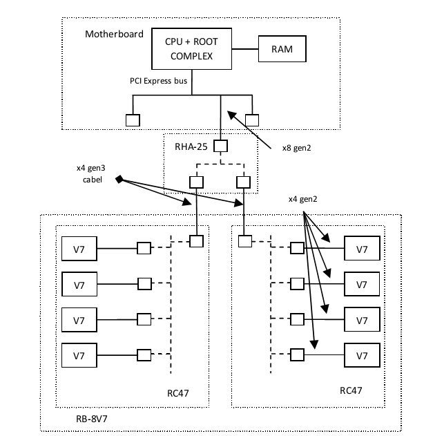
Fig. 1 Hardware. The RB-8V7 unit is connected via cable PCIe connections and the RHA-25 adapter to the host computer
Inside the FPGA, the following scheme was implemented (Fig. 2). The project uses Xilinx's PCI Express IP core (7). The Rosta DMA Engine block determines the functionality of the device on the PCI Express bus. FPGA can act as a master or slave. As a slave device, the FPGA provides the central processor with read and write access to its registers, and can also receive large data packets from other devices on the bus (for example, from other FPGAs) while storing received data in the EP_RX_FIFO queue. As a master device, FPGAs can access the computer’s RAM in DMA (read / write) mode. In this case, when writing to memory, data will be read from TX_FIFO, and when reading from memory, it will be written to RX_FIFO. The device is also able to generate write transactions at an arbitrary address on the bus (for example, to transfer data to other FPGAs), in this case, the data to be transmitted is read from the EP_TX_FIFO queue. The RX_STATE_MACHINE submachine gun is responsible for receiving incoming packets; the TX_STATE_MACHINE submachine is responsible for the transmission of packets. Reception and transmission of packets can go simultaneously. The TX_ARBITER block determines which packet to generate for transmission as follows: absolute priority is given to generating responses during the reading of registers by the central processor, the remaining packets (read / write requests for random access memory or write requests to an arbitrary address) are planned with equal priority (round-robin) . Reception and transmission of packets can go simultaneously. The TX_ARBITER block determines which packet to generate for transmission as follows: absolute priority is given to generating responses during the reading of registers by the central processor, the remaining packets (read / write requests for random access memory or write requests to an arbitrary address) are planned with equal priority (round-robin) . Reception and transmission of packets can go simultaneously. The TX_ARBITER block determines which packet to generate for transmission as follows: absolute priority is given to generating responses during the reading of registers by the central processor, the remaining packets (read / write requests for random access memory or write requests to an arbitrary address) are planned with equal priority (round-robin) .
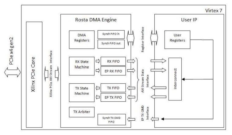
Fig. 2 Block diagram of the FPGA project
The central processor (by writing to the DMA_REGISTERS block) is engaged in programming DMA data transfer between the FPGA and RAM, and there is an internal EP TX CMD hardware interface for controlling the process of writing data to an arbitrary address in another FPGA. For access to user registers in the User IP block, there is a Register Interface, and for block data transfer between the PCI Express space and the user circuit, there are four AXI Stream interfaces connected to the RX_FIFO, TX_FIFO, EP_RX_FIFO, EP_TX_FIFO queues. Finally, towards the PCI Express Xilinx core, the Rosta DMA Engine supports the Xilinx PCIe AXI Stream Interface, which has a width of 64 bits. The unit operates at two clock frequencies: the left side of the circuit at the Xilinx core PCIe frequency (250 MHz), and the right side of the circuit at an arbitrary user frequency. Frequency decoupling occurs through FIFO queues. But in all the experiments described below, the user frequency was equal to the frequency at which the PCIe core (250 MHz) worked.
The User IP block defines the behavior of the device at the application level. In this work, several different schemes were used for different purposes.
Firstly, a circuit was used to verify the correctness of data transfer between the FPGA and RAM. In this case, in the Interconnect block, the output RX_FIFO simply closed at the input TX_FIFO. This made it possible to write exactly the same data to RAM as it was read from it. The program on the central processor (hereinafter simply the host) wrote data to the FPGA, read them, compared and made sure that the data was compared correctly.
Secondly, a circuit was used to measure the maximum data transfer rate between the FPGA and RAM in both directions. For this, from RX_FIFO, the data was constantly read, i.e. the queue was always empty, and there were no delays in receiving data due to its overflow, and TX_FIFO was constantly writing data, i.e. There were no delays in transmission due to a lack of data in the queue.
Thirdly, a scheme was developed to verify the correctness of direct data transfer between FPGAs. In the Interconnect block, the circuit of the outputs RX_FIFO and EP_RX_FIFO and the inputs TX_FIFO and EP_TX_FIFO was implemented. In the first case, the output RX_FIFO was closed to the input TX_FIFO, and the output EP_RX_FIFO to the input EP_TX_FIFO. In the second case, the output RX_FIFO was closed to the input EP_TX_FIFO, and the output EP_RX_FIFO to the input TX_FIFO. This circuit was controlled by a bit from one of the user registers. Registers have been added to the User Registers block to control the EP TX CMD interface. In this case, the host itself controlled the data transfer between the FPGAs, but in general the EP TX CMD interface was designed so that the FPGA circuit itself could initiate data transfer.
Fourth, to measure the maximum data transfer rate between FPGAs, a special scheme was developed that constantly transmits data to EP_TX_FIFO when transmitting data, and constantly reads data from EP_RX_FIFO when receiving data. At the same time, a hardware timer was implemented inside the circuit, the values of which were saved and subsequently sent to the host. The EP TX CMD interface was controlled by the host through user registers.
Finally, to measure latency, a circuit was used that transferred data to another FPGA. The receiving FPGA data immediately wrote them back to the same device. In the transmitting FPGA, a hardware timer was launched at the same time as the transfer started, which stopped at the moment when the data began to enter the EP_RX_FIFO queue. Further, the timer value could be read to the host through user registers.
Linux was installed on the host. Drivers and libraries of our own design were used to work with the equipment.
PCI Express Bus Bandwidth
Before proceeding to the description of experiments on measuring the data transfer rate, it is necessary to find out its theoretical limit. It is known that due to the use of 8B / 10B coding, the maximum theoretical data rate for a single PCI Express line at a frequency of 2.5 GHz (gen1) is V_theory = 2.0 Gbit / s. For the second generation protocol of Gen 2.0 with a frequency of 5 GHz, this speed is 2 times higher (V_theory = 4.0 Gbit / s). The information transfer rate for the third generation is 2 times higher and is equal to V_theory = 8.0 Gbit / s per line (despite the fact that the frequency is 8 GHz, the third generation protocol uses a different 128B / 130B character encoding method that reduces the additional load).
However, the data is transmitted at a slightly lower speed due to the fact that the transmission is in packets that include additional information (start / stop bits, header, checksum, etc.). As a result, when transmitting one packet of a write transaction, in addition to the data, an additional 20 bytes related to the same packet are transmitted. Also, packets are transmitted over the PCI Express bus that do not contain data at all, but perform purely service functions. These include confirmation of the receipt of data packets, requirements to repeat the transmission in the event of a mismatch of the checksum, packets that update the counters of the free space buffers in the switches, and others. It is difficult to accurately assess their effect on the data transfer rate (it depends on the particular implementation), however, on average, their contribution can be approximately estimated as 3 additional bytes per 1 data packet (8). In total, we accept that an average of 23 additional service bytes are transmitted to transmit a single data packet. This is described in more detail in (8). In the future, unless otherwise specified, by the length of the packet we will mean the amount of data in the packet.
On the PCI Express bus, data can be transmitted in packets of different lengths. The maximum amount of data when transmitting one packet is determined by the parameter MAX_PAYLOAD_SIZE, the value of which is equal to the power of two. Each device has a parameter MAX_PAYLOAD_SIZE_SUPPORTED, which determines the maximum packet size that can be transmitted by this device. Configuration software (BIOS program) sets the MAX_PAYLOAD_SIZE parameter for all devices in the system to the smallest of the values supported by devices in the system. As a rule, modern chipsets support packet sizes up to 128 bytes, but there are systems with 256 bytes. In our experiments, the MAX_PAYLOAD_SIZE_SUPPORTED chipset parameter was 128 bytes, and despite the fact that
The larger the size of the transmitted packets, the closer the bandwidth approaches the theoretical limit of information transfer. If the theoretical limit is taken to be 1, then the following formula can be used to calculate the practical limit of data transfer depending on the size of the packet (see Table 1):
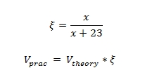
where x is the packet size.
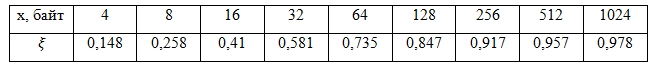
Table 1. Relative data rate versus packet size
. Figure 2 shows a comparison of the maximum theoretical and practical data transfer rates for a packet length of 128 and 256 bytes.
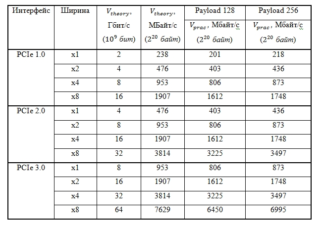
Table 2. Maximum transfer rates of information and data on the PCI Express bus for packets of 128 and 256 bytes length
HOST-FPGA Transmission
When transferring data between FPGAs and system memory, a direct memory access mechanism is used. A user application on the host prepares a buffer in RAM and makes a write or read system call. The PCI Express device driver captures the user buffer pages in memory and uses the scatter / gather DMA mechanism. The list of descriptors (address-length pair) of pages is written to the internal memory of the FPGA device, and then the FPGA itself is accessed by the addresses from this list. After the data transfer is completed, the FPGA generates an interrupt, which completes the system call. When the user application intends to write data to the FPGA, the device contacts the RAM with read transactions, and when reading from the FPGA, the device generates write transactions. Hereinafter, it will be implied throughout that the words “record” and “read” refer to FPGAs, i.e.
Write transactions generated on the PCI Express bus are always unidirectional. The write transaction initiator forms a package consisting of a header and data. The initiator himself determines the size of the data, taking into account only the MAX_PAYLOAD_SIZE restriction. Everything that was said about the data transfer rate in the previous paragraph relates specifically to write transactions. For write transactions, the data transfer rate can be easily estimated theoretically and measure its dependence on the size of the transmitted packet.
With read transactions, things are a little more complicated. The initiator of a read transaction first generates a read request - a short packet consisting only of a header. This package indicates where (from which address) and how much data should be read. The maximum amount of data that can be requested at a time is determined by the MAX_READ_REQUEST_SIZE parameter and is usually 4 KB. Typically, peripherals make read requests in RAM, but can request data from another device. When a device (peripheral or RAM controller) receives a read request, it first requests the required data from its memory, and then returns it to the transaction initiator via the PCI Express bus, generating response completion packets. At the same time, it itself determines the size of the returned packets, again, considering only the MAX_PAYLOAD_SIZE constraint. A transaction initiator cannot affect the size of returned packets. Typically, the RAM controller will return packets with a data length equal to MAX_PAYLOAD_SIZE.
Data transfer rates for read transactions are difficult to evaluate for several reasons. Firstly, two types of packets are generated that move in opposite directions - read requests and final responses. Secondly, the data transfer speed will be affected by delays that occur when reading from RAM. Finally, it is unclear how to trace the dependence of the data rate on the amount of data in the packet. Therefore, in this work, we simply measured the integral time from sending the first read request to the arrival of the last byte of data, using it we calculated the speed of reading data from RAM and did not trace its dependence on the packet size.
The PCI Express bus provides reliable data transfer at the transaction level, i.e., by sending data, agents (terminal devices and intermediate switches) automatically calculate the checksum of the packet, compare it with the encoded one in the packet itself and require retransmission if a transmission error is detected data. However, this does not mean that the host application or FPGA scheme cannot generate and transmit incorrect data as a result of a programmer error. Therefore, to verify the correctness of our circuit, which includes the application, driver, and FPGA circuit, checks were made for the correctness of data transfer. For this, the first User IP scheme was used, in which the RX_FIFO output was closed to the TX_FIFO input. The sizes of the FIFO queues were 4 KB. Two experiments were conducted. In the first, the host sequentially recorded 4 KB of data in the FPGA, then it was read and compared. The second experiment used the fact that the paths for receiving and transmitting data to FPGAs can work in parallel. The host first programmed both write and read operations, and then the FPGA started reading data from RAM, and as soon as it first arrived at RX_FIFO, and then TX_FIFO, it immediately started writing back to RAM. This allowed us to transfer a much larger amount of data at a time compared to the size of the RX_FIFO and TX_FIFO queues (in our experiment, 4 MB). In both experiments, the comparison of the transmitted and received data was successful, which allowed us to judge the correct operation of our circuit. The host first programmed both write and read operations, and then the FPGA started reading data from RAM, and as soon as it first arrived at RX_FIFO, and then TX_FIFO, it immediately started writing back to RAM. This allowed us to transfer a much larger amount of data at a time compared to the size of the RX_FIFO and TX_FIFO queues (in our experiment, 4 MB). In both experiments, the comparison of the transmitted and received data was successful, which allowed us to judge the correct operation of our circuit. The host first programmed both write and read operations, and then the FPGA started reading data from RAM, and as soon as it first arrived at RX_FIFO, and then TX_FIFO, it immediately started writing back to RAM. This allowed us to transfer a much larger amount of data at a time compared to the size of the RX_FIFO and TX_FIFO queues (in our experiment, 4 MB). In both experiments, the comparison of the transmitted and received data was successful, which allowed us to judge the correct operation of our circuit.
The experiments on measuring the data transfer rate began with measuring the dependence of the write speed in the RAM of one FPGA device on the size of the data in the transmitted packets. Experiments were conducted with payload values of 8, 16, 32, 64, and 128 bytes. In each experiment, 4 MB was transferred one way. The bottleneck in the Virtex7 - RAM path was the PCI Express x4 Gen 2.0 connection between the FPGA and the PCI Express switch on the RC47 board (see Figure 1). The results are presented in fig. 3. The upper Vtheory curve represents the theoretical dependence (formula 1) of the maximum achievable data transfer rate on the packet length (for the PCI Express x4 Gen 2.0 interface). The curve in the middle of Vhard represents the speed, measured using a hardware timer in the FPGA and taking into account only data transfer directly on the PCI Express bus (time was measured from the beginning of the transmission of the first packet of data to the end of the transfer of the last). Finally, the Vapp curve represents the speed measured in the application on the host (the execution time of the read system call was measured).
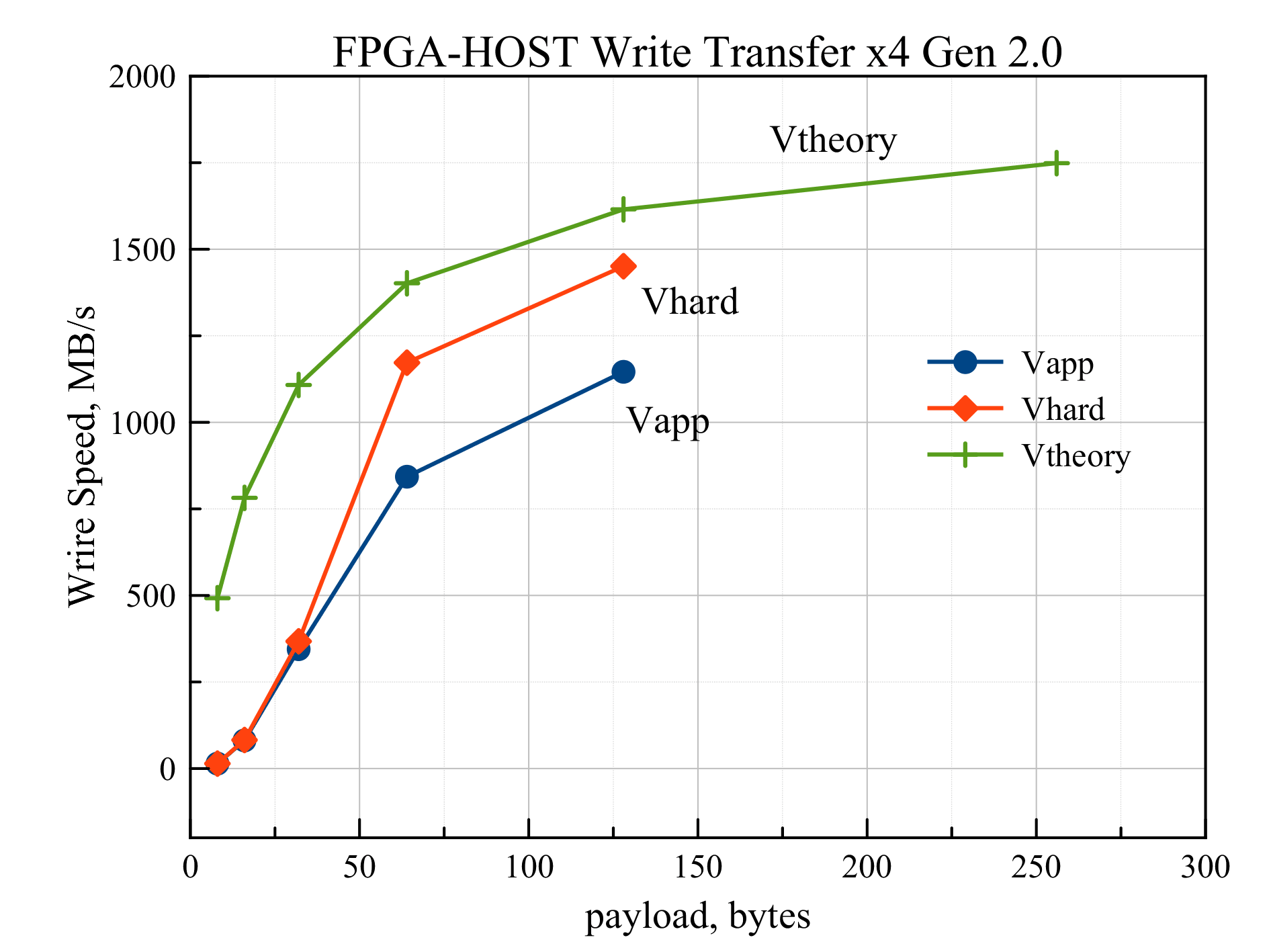
Fig. 3 The dependence of the write speed in RAM on the packet length for the interface PCI Express x4 Gen 2.0
The graph shows that with payload values less than 64 bytes, Vhard and Vapp speeds are much less than Vtheory. This is because in this case, the DDR RAM memory acts as a data receiver, providing high write speed only in burst mode, transferring a large amount of data in one transaction. For a packet of 128 bytes, Vhard = 1451 MB / s, which is 90% of the maximum value of 1612 MB / s. It is also seen that the speed measured in the Vapp application (1146 MB / s with payload = 128) is much lower than Vhard for payload values starting from 64 bytes. This is due to the fact that when transmitting 4 MB of data, about 1000 page descriptors are formed, which the processor writes to the FPGA. This initial delay (of the order of 1 ms) significantly affects the data rate. The total read system call execution time for payload = 128 bytes is approximately 3.7 ms. If we take away the initial delay of 1 ms from this time, then we get a speed of approximately equal to 1450 MB / s, which coincides with the Vhard speed measured in hardware.
Our plans include changing the driver logic and the Rosta DMA Engine circuitry to reduce the initial delay when programming DMA transfers. The idea of the improvement is not to transfer the entire list of page descriptors of the user buffer to the FPGA, but instead to save it in the area accessible to the FPGA in RAM. Then the FPGA itself will be able to read the descriptors from the RAM, on which data will already be transmitted. The process of reading the descriptors from the memory and the actual data transfer can be started in parallel, thereby significantly reducing the initial delay and, as a result, increasing the data transfer speed. In the meantime, we will focus on the speed measured in hardware. Also, in subsequent experiments data transfer with payload less than 128 bytes will not be investigated.
In the next experiment, several data transmissions involving different FPGAs were launched simultaneously. An application on the host started several pthreads threads - one thread per separate transmission. In each thread, the FPGA was first programmed for reading from RAM, and then for writing. Simultaneous transmission was achieved using barrier synchronization in the application. The size of the transmitted buffer was 4 MB, the size of the packets during recording was 128 bytes. The experiment involved all 8 Virtex7 FPGA devices contained in the RB-8V7 unit. The write speeds of data in RAM, depending on the number of simultaneously operating FPGAs, are presented in Fig. 4.
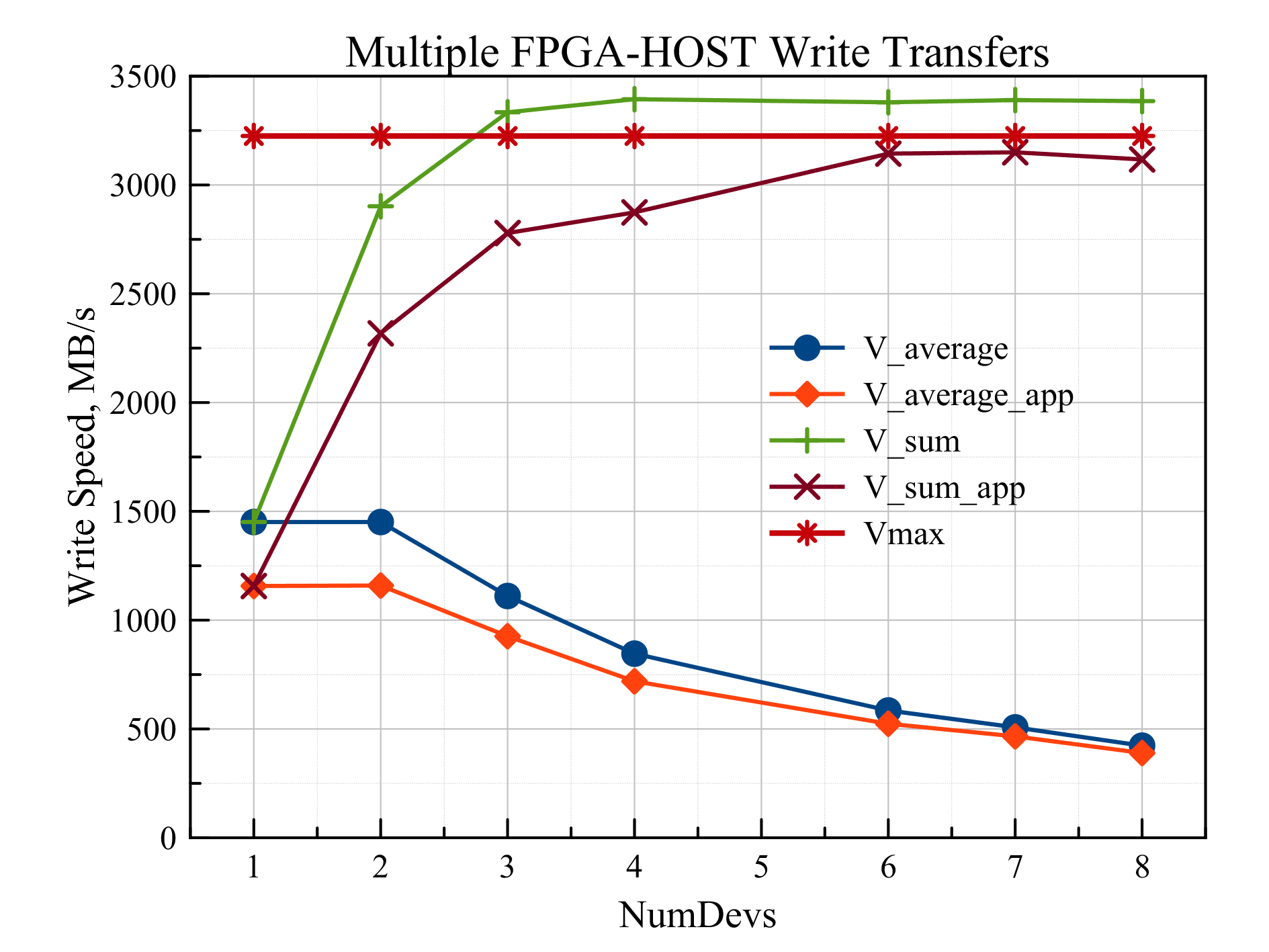
Fig. 4 The dependence of the write speed in RAM on the number of simultaneous transactions
The two lower curves (V_average and V_average_app) show the average write speed, measured in hardware and in the application, respectively. Each individual FPGA is limited in speed to the maximum write speed through the PCI Express x4 Gen 2.0 interface, in our case 1451 MB / s. The V_sum and V_sum_app curves are the sums of the data rates of individual devices. Direct Vmax = 3225 MB / s represents the maximum data transfer rate through the system bottleneck, limiting the speed of simultaneous data transfer. Such a bottleneck is the connection of the PCI Express x8 Gen 2.0 adapter RHA-25 to the computer motherboard. For one and two simultaneous transfers, the write speed is the same (1451 MB / s), because the total speed of two transfers is less than Vmax. Starting with three gears, the recording speed of an individual device drops, however, the total speed is the same and equal to Vmax. The fact that on the graph the total speed for three or more devices exceeds Vmax is explained by the “pseudo-simultaneity” of data transmission. No matter how well the threads are distributed in parallel between the cores of the central processor, the PCI Express bus commands still run sequentially. Therefore, some devices begin transmission earlier, others later. This leads to the fact that for a short period of time at the beginning and at the end of data transfer, the common connection channel of the adapter and the motherboard is not used by all the devices involved in the transfer. Therefore, for them, the transmission speed is greater, and the sum of all speeds exceeds the maximum. In reality, it turns out that the common channel is used at 100%, and the bandwidth is shared between devices in equal shares. that on the graph, the total speed for three or more devices exceeds Vmax, due to the "pseudo-simultaneity" of data transfer. No matter how well the threads are distributed in parallel between the cores of the central processor, the PCI Express bus commands still run sequentially. Therefore, some devices begin transmission earlier, others later. This leads to the fact that for a short period of time at the beginning and at the end of data transfer, the common connection channel of the adapter and the motherboard is not used by all the devices involved in the transfer. Therefore, for them, the transmission speed is greater, and the sum of all speeds exceeds the maximum. In reality, it turns out that the common channel is used at 100%, and the bandwidth is shared between devices in equal shares. that on the graph, the total speed for three or more devices exceeds Vmax, due to the "pseudo-simultaneity" of data transfer. No matter how well the threads are distributed in parallel between the cores of the central processor, the PCI Express bus commands still run sequentially. Therefore, some devices begin transmission earlier, others later. This leads to the fact that for a short period of time at the beginning and at the end of data transfer, the common connection channel of the adapter and the motherboard is not used by all the devices involved in the transfer. Therefore, for them, the transmission speed is greater, and the sum of all speeds exceeds the maximum. In reality, it turns out that the common channel is used at 100%, and the bandwidth is shared between devices in equal shares. due to the "pseudo-simultaneity" of data transmission. No matter how well the threads are distributed in parallel between the cores of the central processor, the PCI Express bus commands still run sequentially. Therefore, some devices begin transmission earlier, others later. This leads to the fact that for a short period of time at the beginning and at the end of data transfer, the common connection channel of the adapter and the motherboard is not used by all the devices involved in the transfer. Therefore, for them, the transmission speed is greater, and the sum of all speeds exceeds the maximum. In reality, it turns out that the common channel is used at 100%, and the bandwidth is shared between devices in equal shares. due to the "pseudo-simultaneity" of data transmission. No matter how well the threads are distributed in parallel between the cores of the central processor, the PCI Express bus commands still run sequentially. Therefore, some devices begin transmission earlier, others later. This leads to the fact that for a short period of time at the beginning and at the end of data transfer, the common connection channel of the adapter and the motherboard is not used by all the devices involved in the transfer. Therefore, for them, the transmission speed is greater, and the sum of all speeds exceeds the maximum. In reality, it turns out that the common channel is used at 100%, and the bandwidth is shared between devices in equal shares. on the PCI Express bus, the commands still go sequentially. Therefore, some devices begin transmission earlier, others later. This leads to the fact that for a short period of time at the beginning and at the end of data transfer, the common connection channel of the adapter and the motherboard is not used by all the devices involved in the transfer. Therefore, for them, the transmission speed is greater, and the sum of all speeds exceeds the maximum. In reality, it turns out that the common channel is used at 100%, and the bandwidth is shared between devices in equal shares. on the PCI Express bus, the commands still go sequentially. Therefore, some devices begin transmission earlier, others later. This leads to the fact that for a short period of time at the beginning and at the end of data transfer, the common connection channel of the adapter and the motherboard is not used by all the devices involved in the transfer. Therefore, for them, the transmission speed is greater, and the sum of all speeds exceeds the maximum. In reality, it turns out that the common channel is used at 100%, and the bandwidth is shared between devices in equal shares. that for a short period of time at the beginning and at the end of data transfer, the common connection channel between the adapter and the motherboard is not used by all devices involved in the transfer. Therefore, for them, the transmission speed is greater, and the sum of all speeds exceeds the maximum. In reality, it turns out that the common channel is used at 100%, and the bandwidth is shared between devices in equal shares. that for a short period of time at the beginning and at the end of data transfer, the common connection channel between the adapter and the motherboard is not used by all devices involved in the transfer. Therefore, for them, the transmission speed is greater, and the sum of all speeds exceeds the maximum. In reality, it turns out that the common channel is used at 100%, and the bandwidth is shared between devices in equal shares.
Similarly, we can consider the case of reading from RAM (Fig. 5).
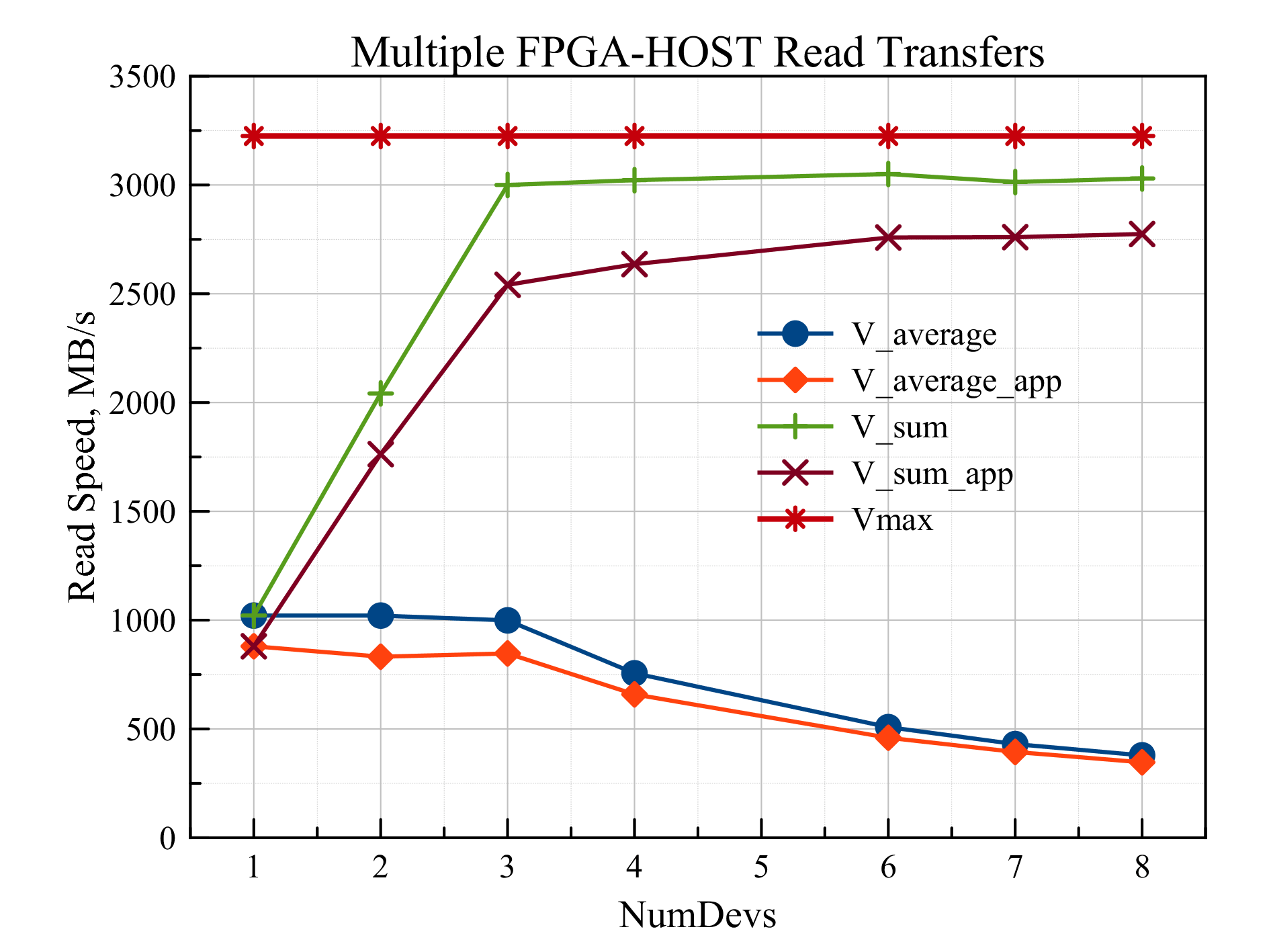
Fig. 5 Dependence of the read speed from RAM on the number of simultaneous transactions.
Here you can see that for data transfer involving one to three devices, the read speed for each device is the same and equal to 1000 MB / s. Starting with four devices, the speed is limited by the bandwidth of the communication channel with the host.
Transmission FPGA-FPGA
Requests for writing and reading memory on the PCI Express bus are sent in accordance with the address encoded in the packet headers. The master is capable of generating a packet with an arbitrary address. This address may indicate in RAM, or may belong to the area of addresses allocated to another peripheral device. In the latter case, the request packet will be sent from one device to another. In our case, write requests between different FPGAs were thus transmitted. No reading tests were performed.
Each FPGA receives from the BIOS or from the operating system a range of addresses at which you can contact this device. In order to program data transfer from FPGA A to FPGA B, the application on the host must inform FPGA A (write in the corresponding register in the User IP block) the base address of FPGA B. In the FPGA in Rosta DMA Engine, the hardware interface EP EP CMD was implemented, intended for initiating data transfer to another FPGA from within the circuit. The circuit writes the data for transmission to EP_TX_FIFO and transmits the base address of the other device and the transmission length via the EP TX CMD interface. Next, the TX_STATE_MACHINE transmitting machine in the Rosta DMA Engine block starts transmitting data from EP_TX_FIFO to the specified address. In the receiving FPGA, data is written to the EP_RX_FIFO queue.
To begin with, it was necessary to verify the correctness of data transfer between FPGAs. For this, the following experiment was performed. The transmission involved a sequence of all 8 Virtex7 FPGAs that are part of the RB-8V7 block (Fig. 6).
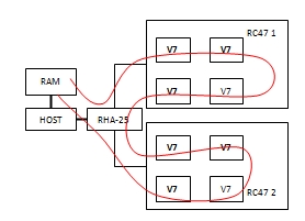
Fig. 6 Data transmission scheme HOST-FPGA-HOST
In the first 7 FPGAs, the host recorded the base addresses of devices according to the following scheme. In the first device - the base address of the second, in the third - the third, and so on. The host programmed the first device to read data from RAM and to transfer read data to the second device. To do this, in User IP, the Interconnect switching unit through User IP registers was configured to connect the output RX_FIFO to the input EP_TX_FIFO. Devices 2-7 were configured to transfer data to the next in the chain. In them, the Interconnect block was configured to connect EP_RX_FIFO to the input EP_TX_FIFO. Finally, the eighth device was programmed to transmit data received in EP_RX_FIFO via TX_FIFO back to RAM. After the transfer, the host compared the data. In this experiment, the data rate in the path was also measured. It was equal to the speed of reading from RAM with one FPGA device.
After making sure that the data transfer was correct, it was possible to proceed to the measurement of speed. Due to the fact that the maximum packet length supported by the chipset was 128 bytes, the MAX_PAYLOAD_SIZE parameter for all switches and terminals in the system was set to 128 bytes. Therefore, by default, data transmission between FPGAs was in packets of the same length. However, it was observed that intermediate PCI Express switches located on the RC-47 boards and RHA-25 adapter, as well as PCI Express interfaces inside the FPGA, supported a packet length of 256 bytes. At the same time, the chipset itself did not participate in the transfer of data between FPGAs. It was suggested that if you configure MAX_PAYLOAD_SIZE for all devices in the FPGA-FPGA data path equal to 256, you can start transmitting packets of 256 bytes in length, despite the fact
To change the MAX_PAYLOAD_SIZE parameter using Linux, the setpci command was used to write to the PCI Express Device Control register for all devices and switch ports on the RHA-25 and RC-47 boards. The Rosta DMA Engine block has also been modified so that packets of 256 bytes can be generated. After which it was really possible to organize data transfer from pancake packets 256, and the data transfer rate increased.
FPGA-FPGA recording speed measurements were carried out for different numbers of simultaneous transmissions. The results are presented in table 3.
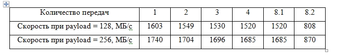
Table 3. The dependence of the recording speed of the FPGA-FPGA on the number of simultaneous transmissions with packet lengths of 128 and 256 bytes.
In the first four cases, transfers went between devices on the same RC47 board. The maximum write speed was obtained during one data transfer and amounted to 1603 MB / s for a packet length of 128 bytes and 1740 MB / s for a packet length of 256 bytes. In both cases, the speed was 99% of the maximum possible for the corresponding packet length.
Device interaction schemes for cases 8.1 and 8.2 are presented in Fig. 7.
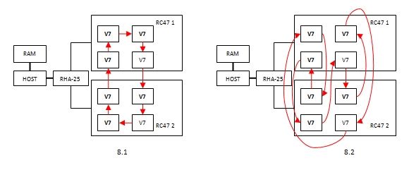
Fig. 7 FPGA interaction in case of 8 simultaneous transfers
In case 8.1, the data was transmitted sequentially from the FPGA to the FPGA, first in a circle on one board, and then through an external cable connection and the RHA-25 adapter, transmission continued to the FPGA on the other board. On the second board, the data was also sequentially copied from one FPGA to another, and then returned to the first. As a result, through the RHA-25 adapter, one data transmission went to each side, and the PCI Express x4 Gen 3.0 cable connection did not limit its speed in any way. In case 8.2, data was transferred from one FPGA to another, but located on another board. As a result, there were 8 simultaneous transmissions through the RHA-25 adapter, 4 in each direction. For a packet length of 128 bytes, the speed of the general data flow in one direction was 4 * 1520 = 6080 MB / s, which exceeds the maximum speed for the PCI Express x4 Gen 3.0 channel equal to 3225 MB / s. Therefore, the channel speed should have been divided equally between devices, and the average data transfer rate in each pair should have become 3225/4 = 806 MB / s. This is confirmed by a measured value of 808 MB / s. Therefore, it can be argued that the communication channel between the boards turned out to be 100% engaged. The same reasoning can be made for transmitting packets with a length of 256 bytes.
Finally, an experiment was conducted to measure data transmission latency. The idea of the experiment was as follows. FPGA A sends data to FPGA B and starts the hardware timer. The clock in different devices is difficult to synchronize, so the timer is used only in FPGA A. As soon as FPGA B receives data, it immediately starts to write them back to FPGA A. The timer stops as soon as FPGA A receives the first byte of data. The timer value represents the doubled latency of data transfer between the User IP block of one FPGA and User IP of the other. Latency was measured in two cases: during transmission between FPGAs on one RC-47 board (Fig. 8 A) and between FPGAs on different boards (Fig. 8 B).
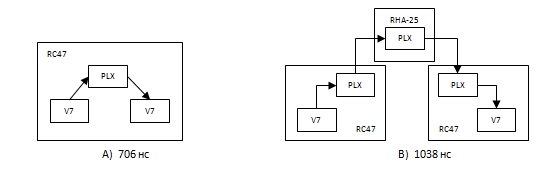
Fig. 8 Data transmission schemes for measuring latency
When transferring data between devices on one RC-47 board, there was one PLX switch in the transmission path, and the delay was 706 ns. When transferring from board to board, there were three intermediate switches, and the delay was 1038 ns. From this data, you can determine the delay that occurs in the FPGA and introduced by the switch. The delay in the FPGA at the reception and transmission turns out to be equal to 270 ns, and in the switch 166 ns, which is in good agreement with the latency of the switches declared by PLX Technology of 150 ns.
Conclusion
In this paper, the data transfer via the PCI Express bus with the simultaneous participation of several FPGAs was described. When writing to RAM, a speed equal to 90% of the maximum for a PCIe x4 Gen 2.0 connection was obtained with a packet length of 128 bytes (1451 MB / s). When reading from RAM, the speed was 1000 MB / s. In the case of simultaneous FPGA-HOST transmissions, the data transfer rate did not decrease until the number of simultaneous transmissions saturated a narrow channel of communication with the host, in the future the channel was used at 100%, and its bandwidth was shared evenly between devices.
During the FPGA-FPGA transmission, it was possible to start the exchange of 256-byte packets, although the host computer's chipset only supported 128. In this case, we managed to get a speed of 1740 MB / s, which is 99% of the maximum transfer speed of the PCI Express x4 Gen 2.0 interface with a length 256 byte packet. It was also shown that it is possible to start several simultaneous FPGA-FPGA transmissions, and while the total transmission speed does not exceed the bandwidth of the common channel, the speed of individual transmissions does not decrease, and then the channel is used by 100%, and its bandwidth is divided equally between devices.
The FPGA-FPGA data transmission latency was measured, which was 706 ns for one intermediate switch and 1038 ns for three.
All this allows us to consider that the approach based on the use of FPGA and IP core of PCI Express Xilinx interface and PLX Technology switches can be effectively used to organize data exchange between a large number of FPGAs connected to the local PCI Express bus of a computer.
List of references
1. Rosta LTD, 2013. www.rosta.ru .
2. nVidia Corporation. GPUDirect developer.nvidia.com/gpudirect .
3. Ra Inta, David J. Bowman, Susan M. Scott, “The“ Chimera ”: An Off-The-Shelf CPU GPGPU FPGA Hybrid Computing Platform, International Journal of Reconfigurable Computing, 2012.
4. Bruno da Silva, An Braeken, Erik H. D'Hollander, Abdellah Touhafi, Jan G. Cornelis, Jan Lemeire, «Performance and toolchain of a combined GPU / FPGA desktop», Proceedings of the ACM / SIGDA international symposium on Field programmable gate arrays, 2013.
5 Ray Bittner, Erik Ruf, Alessandro Forin, “Direct GPU / FPGA Communication Via PCI Express,” Cluster Computing, 2013.
6. Sunita Jain, Guru Prasanna, “Point-to-Point Connectivity Using Integrated Endpoint Block for PCI Express Designs”, Xilinx Corporation, XAPP869, 2007.
7. 7 Series FPGAs Integrated Block for PCI Express v1.7 Product Guide, Xilinx Corporation 2012.
8. Alex Goldhammer, John Ayer, “Understanding Performance of PCI Express Systems,” Xilinx Corporation, WP350, 2008.