The panel from "Dendy" in amateur designs
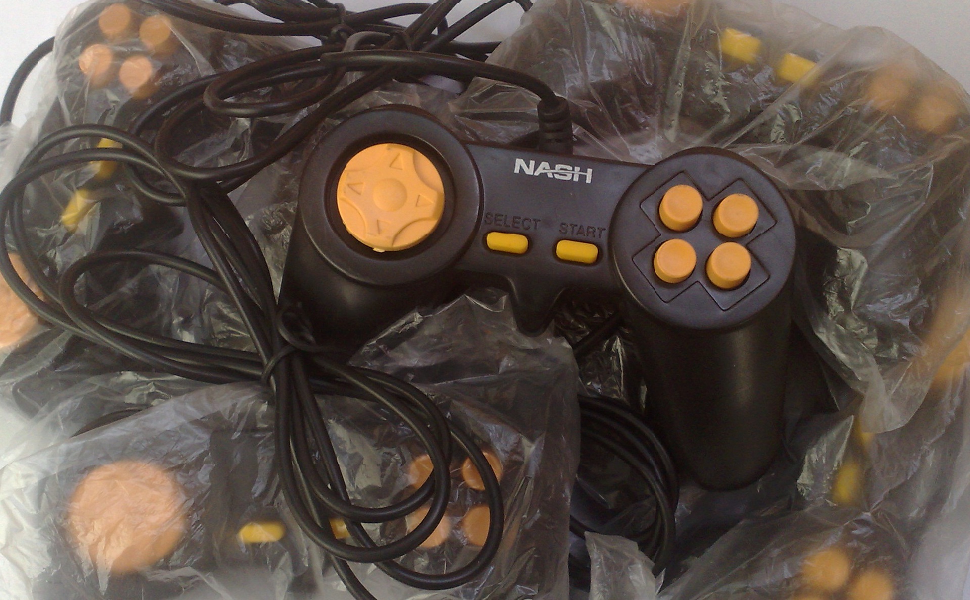
Often, radio amateurs are faced with the problem of designing a remote control panel for the device. If the number of buttons on it is large, then to reduce the number of wires in the connecting cable, the console is equipped with an encoder for the commands of the pressed buttons, and the device is equipped with a decoder. In this situation, the old joystick, from the once popular Dendy game consoles, can help out. The task of the radio amateur is greatly simplified, since the joystick has a good design and is equipped with a ready-made encoder for pressing buttons.
What's inside the joystick?
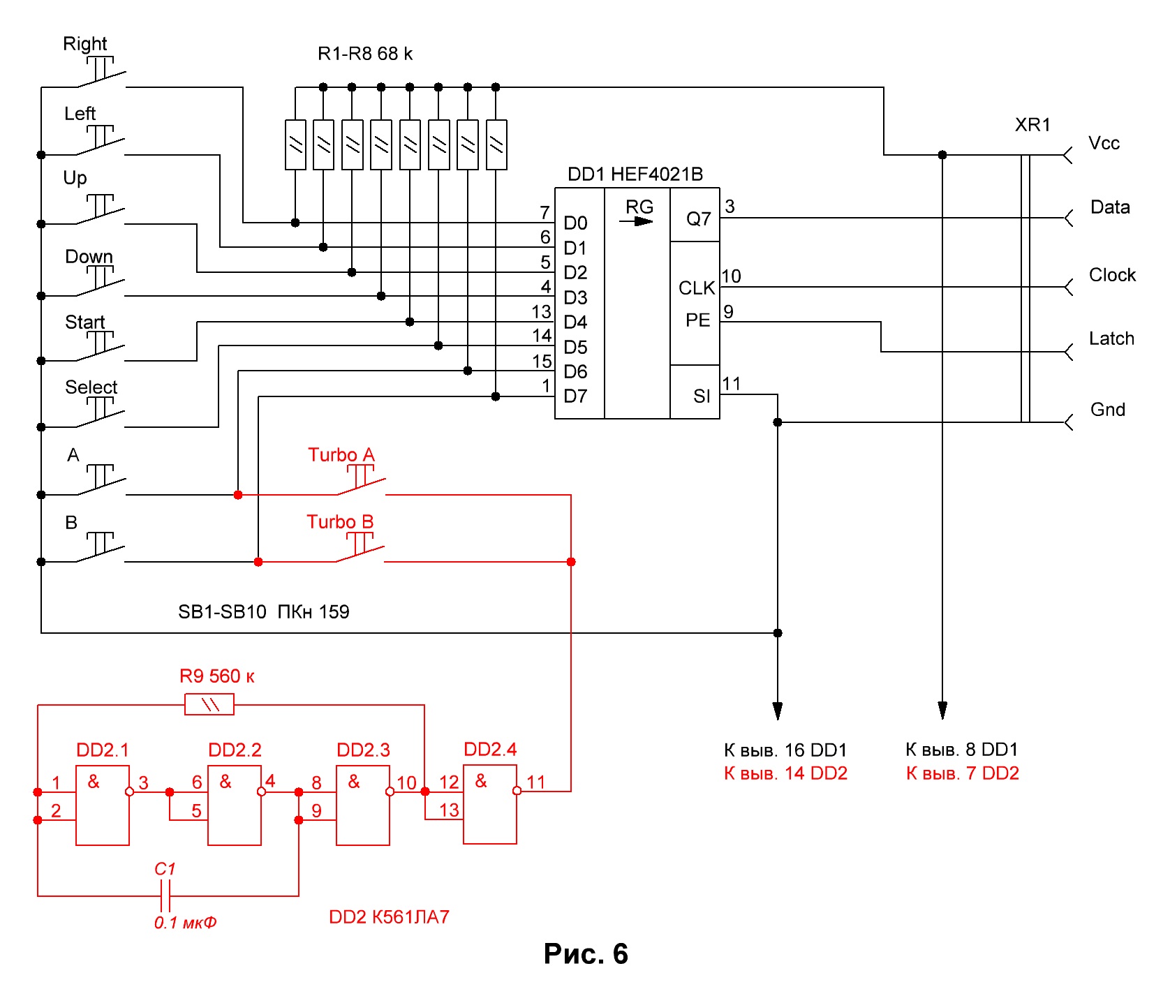
An example scheme of the encoder used in the Dendy joysticks is shown in Fig. 6 , at the end of the article. Information about the interface between the joystick and the game console, a variant of the joystick scheme, and also variants of the decoder schemes can be found on the pages of the Radio magazine. [l] Information on the pressed buttons of the joystick is transmitted in sequential format using the clock signal “Clock” from the controlled device. To synchronize with it, the joystick has an input “Latch”, which receives a short pulse with a high logical level at the beginning of each cycle of receiving data from the joystick.
Decoder device and its operation
The proposed device, the electrical circuit diagram of which is shown in Fig. 1 , is a decoder that converts the joystick signals to discrete logic levels corresponding to the pressed buttons.

Its base is the 74HC595N (DD3) chip, which is an 8-bit shift register with serial input and serial and parallel output of information. The parallel output of information is carried out through a buffer register with outputs that have three states. The information signal is fed to the SER input (pin 14), the write signal to the SCK input (pin 11), and the output signal (“latch”) to the RSK input (pin 12). This register receives a byte that carries information about the pressed buttons, sequentially, and outputs to outputs Q0 - Q7 in parallel. Thus, the state of each individual output, the output register of the microcircuit, will correspond to the button assigned to it on the joystick. The correspondence between the register pins and the joystick buttons is shown in the table below .

On the DD2 chip, the “Latch” clock driver is assembled, which is necessary for fixing the state of the buttons on the joystick and outputting the most significant bit of data from the joystick to the “Data” output. This happens, on the positive front of the impulse. On the negative edge of this pulse, a data byte read cycle begins. This moment is designated as the “joystick polling cycle” (see Fig. 2) The next bits in order will be issued to the “Data” output with the appearance of a positive edge of the clock pulse, at the “Clock” input of the joystick. Also, the “Latch” clock pulse is fed to the RSK input of the shift register, this is necessary to “click” the received byte in the output register and output it to the outputs Q0 - Q7 in parallel. The “latching” of the received byte occurs along the positive edge of the pulse. This point in time is designated as the “information update cycle at the output of the 74НС595 register” (see Fig. 2 ). With the arrival of each clock, the information at the output of the register will be updated.
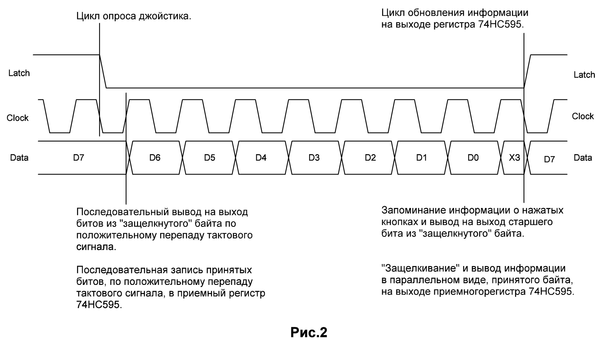
On the DD1 chip, a clock generator is assembled. The frequency of which is 100 kilohertz. Clock pulses are fed to the “Clock” input of the joystick and to the SCK input of the receive register 74НС595. Data on the state of the joystick buttons is output to the “Data” output in order, starting with the high bit - D7, D6 ... D0. This happens on the positive edge of the clock pulse at the input "Clock" of the joystick. The bits read from the “Data” output are fed to the input of the SER register 74НС595. The received bit is also written to the register along the positive edge of the pulses of this generator.
- dude! You have the moment of updating the bit of information at the output of "Data" combined with the moment of reading the set bit at the output of "Data"!
“Yes ... that's for sure.” But the joystick is quite “braking”, and the update of the bit, after the arrival of a positive edge of the clock pulse, occurs after 120 nC. While the joystick is thinking, the fast 74NS595 manages to record the previous value from the “Data” output, for 20 nC.
- uh, "Kulibin!" During the duration of the “Latch” pulse, garbage is written to your 74NS595 output register - two bits of D7 in a row!
- Yes, I admit - hack. But after the end of the write cycle of the entire byte, the extra bits will "fall out" of the register to nowhere, and will not affect the accuracy of the received information.
SPI Interface
And one more thing ... Many, looking at the picture ( Fig. 2 ), saw a similarity with the timing of the SPI communication interface. Yes yes yes ... for some differences, this is it! It is necessary to change the signal names: “Latch” to CS or SS, “Clock” signal to CSLK or CLK, “Data” signal to MISO, SDO or SO (as you like). The joystick can be interrogated by the integrated peripheral module SPI in the MK. To do this, send bytes to the device, no matter which, for example, FF.
True, if this byte can be useful to someone, it can be loaded with the necessary information. For example, for a register with LEDs. Or do not download, but forward the received information from the joystick to someone else. That is, the MOSI pin can be used .
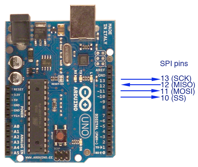
The received byte will contain information about the buttons pressed. The pressed button will correspond to a bit equal to zero, and not the pressed unit. If no button is pressed on the joystick, then the FF byte will be received, if it manages to hold all the buttons at once, the received byte will contain 00. The SPI interface must be configured to work in Master mode, well, that’s clear ... and set the synchronization mode to CPOL = 1, CPHA = 0 (Mode 2). In this situation, the data from the “Data” output (MISO for MK) will be read out by the microcontroller based on the negative edge of the CSLK clock signal applied to the “Clock” input of the joystick. And the update of the information bit at the “Data” output of the joystick and at the MISO input of the microcontroller will occur on the positive edge of the clock pulse. In the same way, the joystick can be connected to the Arduino board.
Turbo A and Turbo B
Earlier joystick models contained 8 buttons, later ten. Two buttons “Turbo A” and “Turbo B” were added. But on the data exchange protocol, this did not affect in any way - it remained the same. The added turbo buttons are equivalent to the “A” and “B” buttons, with the only difference being that when the “Turbo A” button is pressed, the “A” button will be pressed, only at a speed of 12 and a half times per second. This is also true for the Turbo B and B buttons. The turbo click generator was added to the joystick itself (see Fig . 6 , highlighted in red). When the turbo buttons are pressed, outputs Q6 and Q7 of the DD3 register will have pulses with a period of 80 ms and a duty cycle of two.
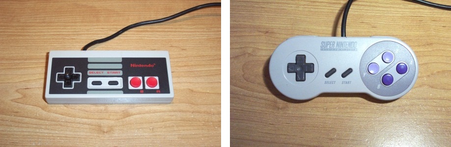
There are joysticks with even more buttons, as well as smaller ones. Pressing additional buttons on such joysticks is equivalent to pressing two buttons at once on older models. When connecting control LEDs to the decoder, it will not be difficult to understand the operation of the “super joystick” buttons.
UPD: Regarding SNES.
In the comments to the article it was rightly noted:
In the text we are talking about a turbo click generator, and to it comes a picture with joysticks where there is no such generator. Below it is written “Pressing additional buttons on such joysticks is equivalent to pressing two buttons at once on older models”, but this is also unfair to SNES.
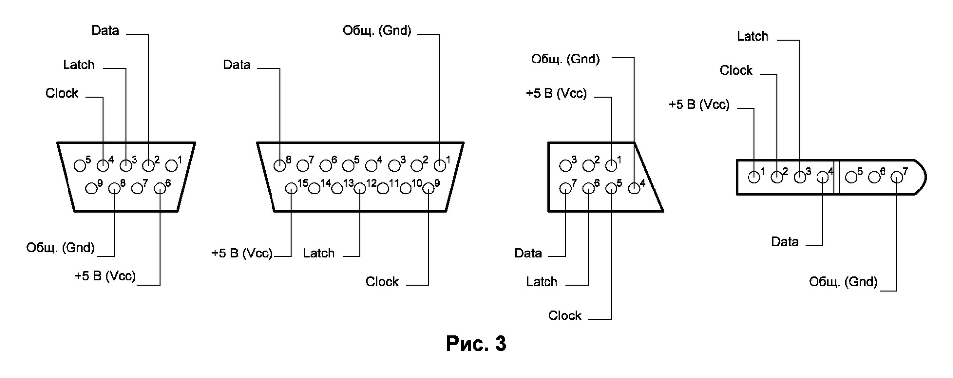
There are no turbo generator clicks in SNES joysticks. That is, you will not see any pulses at the output of the decoder, when you connect such a joystick. Not only that, the SNES protocol is not radical, but different from the NES protocol. The difference is that it is 16-bit. Informative bits only - D15 - D4, bits D3 - D0 are always equal to one. When connecting such a joystick to the proposed decoder, you will receive information about the buttons: “B”, “Y”, “Select”, “Start”, “Up”, “Down”, “Left” and “Right”. Information about the buttons: “A”, “X”, “L” and “R”, will be lost. The SNES connector is shown in fig. 3 rightmost.

UPD: The Good That Turbo Gives Us
Probably someone, having read about the pulses at the decoder output when the “Turbo A” and “Turbo B” buttons are pressed, was upset:
- Uh ... so the Turbo buttons cannot be used, it’s a shame, the two buttons are lost.
- Not! They are not lost at all.
Let's imagine that when controlling a device, you need to increment a parameter in the direction of increasing or decreasing it. If at the same time a high discreteness of setting the value is required, then you can get tired of squeezing the buttons “plus” and “minus”, let them be buttons “A” and “B”. This is where the turbo buttons come in handy. When using the joystick in conjunction with the microcontroller, you will be spared from writing an extra piece of program code, because you no longer need to cram the advanced interface functionality into two buttons. It has already been expanded to four, and is equipped with a logic of work.
Interface SNES, NES
Together with the proposed decoder, you can use any joystick that has an SNES, NES, or Virtual Boy interface. And also their numerous clones - "Dendy",
Connecting devices to the decoder
The signals at the decoder output correspond to TTL levels. The button pressed on the remote control corresponds to - high level, low - not pressed. If the device connected to the decoder is matched according to TTL levels, then additional measures for coordination are not required.
If inverter output requires inverse signal states (the button is pressed - zero, the button is not pressed - one), then the DD1.4 element ( Fig. 1 ) must be excluded from the circuit.
In those cases when the devices connected to the decoder cannot be controlled by logic levels or galvanic isolation on the power is required, use a relay or optocoupler fig. 4 a, b .
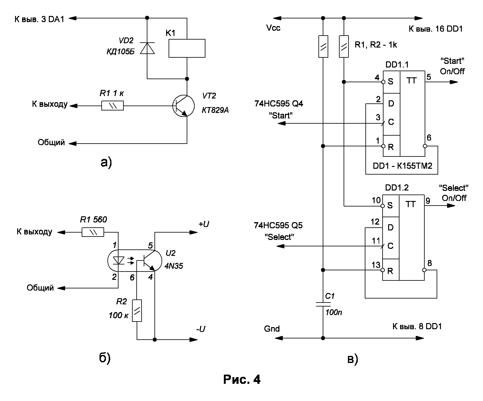
If control of something requires static type control signals (the button is pressed, the couple are turned on there, pressed again, turned off), the device must be supplemented with a trigger. Using one K155TM2 chip (see Fig. 4 c ), the “Start” and “Select” buttons can be turned into switches. Perhaps here the effect of bounce of contacts will appear (if suppression is not implemented in the joystick itself). In this case, it is necessary to reduce the frequency of the clock generator, for example, to 100 hertz. In this case, the joystick will be interrogated 10 times per second, and the problem of bounce will be solved.
Device design
Most parts are mounted on a printed circuit board made of single-sided foil-coated fiberglass with a thickness of 1 ... 1.5 mm, a drawing of the printed circuit board is shown in Fig. 5 . LEDs can be installed only at the setup stage, for clarity.
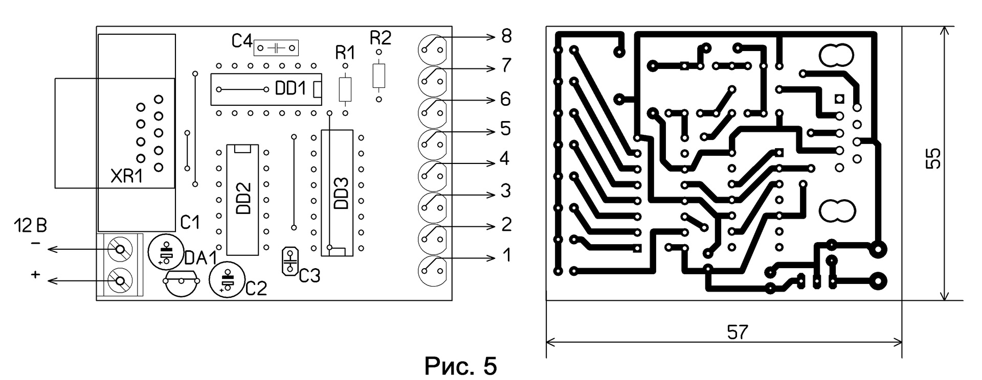
The device uses a resistor C2-23, MLT, a film capacitor C4 - K10-17, a ceramic capacitor C3 - KM-6, oxide capacitors C1, C2 - K50-35 or imported analogues of the listed types of parts. The XR1 connector was borrowed from a failed DVD player. In the absence of the original connector, the device must be equipped with any other, suitable in design and overall dimensions. They feed the device from a 12 V power supply and a current of 50 mA.
UPD:If suddenly someone comes in handy, then according to the NATO classification: DD2 - SN7493, DD1 - SN7400, this will be the 155th series. Or SN74LSxx it will be a 555 series, but in general put everything you find, the main thing is that there are numbers 93, 00 and 74.
Literature:
Joystick Dendy - remote control
S. KULESHOV, Kurgan
. Radio Magazine No. 4 of 2002.
Decoders of joystick teams from video game consoles
S. RYUMIK, Chernigov, Ukraine
Radio Magazine No. 6 of 2004.
Repair of the Dandy joystick "
S. Golubev, Omsk.
Magazine" Radio "No. 6 1996.
PS.
If anyone needs it - here's the board. (archive is hidden in the picture)

For movie lovers, I found some kind of video report - they say, the scheme for ointment ...