UEFI BIOS File Device, Part One: UEFI Capsule and Intel Flash Image
- Tutorial
The release of motherboards on Intel chipsets of the sixth series (P67 and its brothers) brought to the mass market of PCs a new BIOS option - UEFI . In this article we will talk about the UEFI Capsule and Intel Flash Image file device.
The structure of EFI Firmware Volume and useful patches in the household will be described in the second part.
As an example of a UEFI Capsule file, take the BIOS image for ASUS P8Z77-V version 2003.
This is a typical representative of the AMI Aptio4 UEFI family with several ASUS extensions that do not greatly affect its format. It is taken as an example because it contains all the components of the UEFI Capsule file that I would like to talk about today.
To work with this file in the first part of the article we need:
Having unpacked the archive, we get a file of size 0x800800 bytes with a CAP extension.
This is a UEFI Capsule file, the format of which was described by AMI at one of the UEFI Plugfest conferences and looks like this:

Open the file with a hex editor and check it for compliance with this format, in our case the header looks like this: The

size of the header is really 0x0000001C, the total file size is really 0x00800800 , the beginning of the FFS image is really at offset 0x800 - there is no doubt.
Immediately there is a temptation to understand thoroughly exactly how the FW Certificate and OEM Header blocks are arranged, but this is not necessary. We do not have an ASUS private key yet, and without it it is impossible to sign a modified file, even knowing the format of the FW Certificate block, and hacking the RSA2048 and SHA256 is bad.
In fact, this format is not kept secret by anyone, it is described by the WIN_CERTIFICATE structure familiar to PE32 + experts, a description of which can be found, for example, here , but in our case this is not important.
Not a single byte from this two-kilobyte header falls into the BIOS chip, and this header is used only to verify the validity of the file before flashing with standard ASUS utilities. When flashing with a hardware programmer, as well as low-level utilities like the Intel Flash Programming Tool or flashrom, this header just needs to be deleted.
Moreover, the microcontroller that performs firmware using UBF technology , although it checks for the presence of this header, does not check the certificates and flashes the modified files no worse than the original ones.
Therefore, if UBF will not be used for firmware, we safely cut off the 0x800 byte of the header and save the resulting file with the ROM extension.
If there is no UEFI Capsule header in your BIOS file, then it is either old enough, for example, for a P67 or Z68-based board, or the manufacturer did not want to use it, despite Intel's persistent recommendations. Consider that the manufacturer has already deleted it for you and read on.
And then there may be several options.
If you have a desktop board on Intel, as in our example, then the resulting file will consist of several regions: a descriptor, a GbE region with an integrated Intel network card, the ME region, and the BIOS region.
If you have a desktop board or laptop with AMD, then only the BIOS region remains of all the above.
If you have a laptop with Intel, then the BIOS file, which you can download from the manufacturer’s website and use it for updating, most often contains an image of only the BIOS region and firmware for the EC, which is usually stored in a separate flash chip. The file itself can be quite cunningly structured or encrypted, but at the same time it is stored in the BIOS chip in the same form as on desktop boards, so it’s better to conduct all the experiments not with the update file, but with a dump of the existing BIOS, which can be removed using FPT .
AMD's can safely skip the entire text below and read the second part of this article, and we continue to parse the resulting ROM file.
Intel talks about the structure of its BIOS on the datasheet pages for the corresponding chipsets. For all chipsets, starting with the 6th series, this format has not generally changed, so you can safely take it from there. The file is divided into 3-5 regions: The

optional regions are GbE (used in conjunction with entry-level Intel integrated network cards) and PDR (intended for OEM data, but I have never seen it used somewhere).
This region should be located in the first (of two supported) flash chip at the zero address and is divided into 11 sections, the total size of which should not exceed 4 kilobytes. It is arranged like this:

The first 16 bytes are not used and are always equal to 0xFF, followed by the signature 0x0FF0A55A, then the Descriptor Map section, indicating the offset of the initial five sections and their size.
The Component section contains information about the used flash microcircuits: their number (1 or 2), density (from 512 Kb to 16 Mb), prohibited commands (such as chip erase, for example) and read, fast read and erase / write frequencies.
The Region section contains offsets and sizes of other regions.
The Master section contains access settings for each of the three possible masters (BIOS, ME, GbE) to five possible regions.
The PCH / PROC Straps sections contain processor and northbridge configuration options.
The Upper Map section contains the offset and size of the VSCC table .
The VSCC table contains the JEDEC IDs and VSCC data of all flash chips supported by the Management Engine.
The OEM section can be filled by OEMs at its discretion, but I have never seen it filled.
Now let's check the structure of the ROM file we received for compliance with the above:

It is easy to see that the structure is quite consistent with itself, but guessing what exactly each byte of each section is responsible for will not be easy.
Fortunately, Intel saved us from guessing by releasing the FITC utility., which allows you to configure the descriptor (and not only it) and contains hints for each item available for editing. This utility is included in the kit for motherboard developers and is not intended for end users, but a link to it can always be found on the forums devoted to BIOS modifications.
We open our ROM file in FITC 8.xx and all the descriptor settings at a glance:
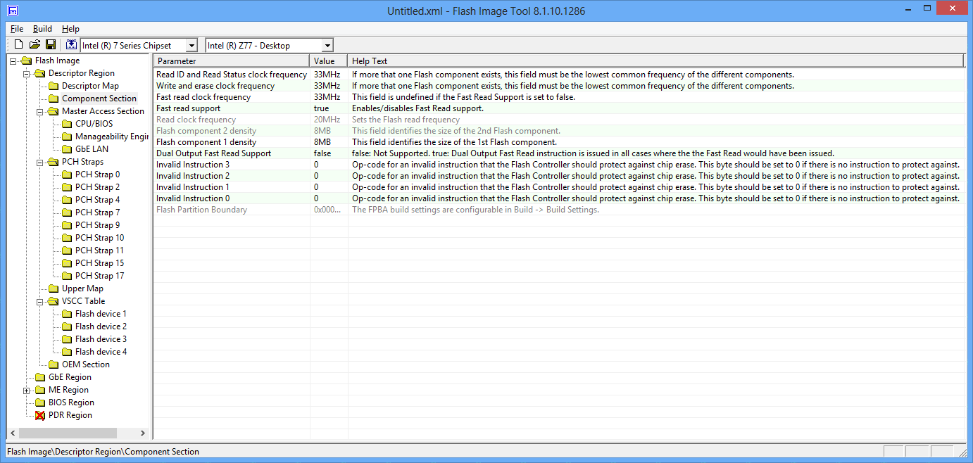
I highly recommend not changing anything, who does not know why he does it.
The most frequently changed settings here are the settings for access to regions (highlighted in green on the screenshot of the hex editor), which in the wild are of two types: the above “everything is possible for everyone” and the standard Intel settings. Sometimes the openness of recording in the ME region helps to cope with the violation of its performance by simply overwriting it completely. On boards with standard settings, this is impossible without gaining access to ME, which is implemented differently on different boards and may require quite nontrivial manipulations (closing the legs of the audio chip during boot, for example).
The flip side of openness is that malicious code can do anything with a descriptor and all other contents of the BIOS chip. For some reason, it’s not accepted to talk about this, despite the fact that absolutely all ASUS motherboards on P67 with BIOS versions 3xxx and all ASUS motherboards on Z68 have an open descriptor. And there is no security, and with obscurity the problems that the engineers were thinking about do not know.
The second useful setting is the density of the BIOS chip, which has to be changed if the damaged BIOS of a board with a chip with a large volume is restored using a workable board with a smaller chip.
It is present only on boards with integrated Intel network cards of the entry level, such as 82579.
In the datasheet for this chip, in section 10 there is a description of the NVM structure , which is stored in the entire GbE region.
The main setting, which may be interesting to change, is the MAC address, located at the very beginning of the region, in the first 6 bytes. If you suddenly need to change the hardware MAC of your integrated Intel card, and there is a GbE region on your board, you know what to do.
In our example, the GbE region is located at an offset of 0x1000 from the beginning and contains the standard MAC for all NVM images released by Intel as an update - 88: 88: 88: 88: 87: 88:

When flashing with standard tools, the GbE region is not updated at all, despite the presence of the updated NVM in the BIOS update file, so Intel had to issue a separate NVM Update utility when, as a result of an error in version 1.3, the card stopped working normally after installing Windows 8.
The region contains a bunch of other settings that you can read about in the datasheet above.
Here is the Management Engine Firmware and its settings. About ME you can write endlessly, because there is nothing there. You can read the best description of the structure of this region and possible attack vectors on it in a report by Igor Skochinski at Breakpoint 2012 .
For those who have not gone to read it - a brief squeeze:
Intel chipsets have a microcontroller with ARCompact architecture, which is powered by the ATX standby line, has access to all devices, RAM, its own network stack and runs under ThreadX RTOS. So it provides all the technologies advertised by Intel, such as Active Management, AntiTheft, Identity Protection, Rapid Start, Smart Connect, Protected Audio Video Path, and so on and so forth. And with the help of the Dynamic Application Loader, you can even run Java applets on it.
Fortunately for me, the security of ME is more or less in order, and so far I have not heard about cases of successful implementation of malicious code, but the mere presence in the chipset of MK, executing programs unknown to anyone except Intel, and having full access to RAM and networks are already an occasion for paranoia among people prone to it.
You can change the available ME settings using the same Intel FITC:

In our example, the ME region begins with an offset of 0x3000 and has a size of 1.5 MB, which indicates a board without AMT support .
A region consists of one or more EFI Firmware Volume, the structure of which I will write in the second part of this article.
There we will cover the UEFI boot process and patches useful in some cases.
The region is intended to describe any platform-specific capabilities and should be used by OEMs according to the plan, but in fact I have never seen it.
I don’t know in which hub this article should be placed. Maybe a UFO will create a UEFI hub for us?
I look forward to your comments and apologize for possible errors, which I ask you to report in a personal message.
Thank you and see you in the second part.
The structure of EFI Firmware Volume and useful patches in the household will be described in the second part.
UEFI Capsule
As an example of a UEFI Capsule file, take the BIOS image for ASUS P8Z77-V version 2003.
This is a typical representative of the AMI Aptio4 UEFI family with several ASUS extensions that do not greatly affect its format. It is taken as an example because it contains all the components of the UEFI Capsule file that I would like to talk about today.
To work with this file in the first part of the article we need:
- Hex editor to your taste, I will use HxD
- Intel Flash Image Tool utility of the appropriate version, for chipsets of the 7th series - this is version 8.xx
Having unpacked the archive, we get a file of size 0x800800 bytes with a CAP extension.
This is a UEFI Capsule file, the format of which was described by AMI at one of the UEFI Plugfest conferences and looks like this:
Open the file with a hex editor and check it for compliance with this format, in our case the header looks like this: The
size of the header is really 0x0000001C, the total file size is really 0x00800800 , the beginning of the FFS image is really at offset 0x800 - there is no doubt.
Immediately there is a temptation to understand thoroughly exactly how the FW Certificate and OEM Header blocks are arranged, but this is not necessary. We do not have an ASUS private key yet, and without it it is impossible to sign a modified file, even knowing the format of the FW Certificate block, and hacking the RSA2048 and SHA256 is bad.
In fact, this format is not kept secret by anyone, it is described by the WIN_CERTIFICATE structure familiar to PE32 + experts, a description of which can be found, for example, here , but in our case this is not important.
Not a single byte from this two-kilobyte header falls into the BIOS chip, and this header is used only to verify the validity of the file before flashing with standard ASUS utilities. When flashing with a hardware programmer, as well as low-level utilities like the Intel Flash Programming Tool or flashrom, this header just needs to be deleted.
Moreover, the microcontroller that performs firmware using UBF technology , although it checks for the presence of this header, does not check the certificates and flashes the modified files no worse than the original ones.
Therefore, if UBF will not be used for firmware, we safely cut off the 0x800 byte of the header and save the resulting file with the ROM extension.
If there is no UEFI Capsule header in your BIOS file, then it is either old enough, for example, for a P67 or Z68-based board, or the manufacturer did not want to use it, despite Intel's persistent recommendations. Consider that the manufacturer has already deleted it for you and read on.
And then there may be several options.
If you have a desktop board on Intel, as in our example, then the resulting file will consist of several regions: a descriptor, a GbE region with an integrated Intel network card, the ME region, and the BIOS region.
If you have a desktop board or laptop with AMD, then only the BIOS region remains of all the above.
If you have a laptop with Intel, then the BIOS file, which you can download from the manufacturer’s website and use it for updating, most often contains an image of only the BIOS region and firmware for the EC, which is usually stored in a separate flash chip. The file itself can be quite cunningly structured or encrypted, but at the same time it is stored in the BIOS chip in the same form as on desktop boards, so it’s better to conduct all the experiments not with the update file, but with a dump of the existing BIOS, which can be removed using FPT .
Intel Flash Image
AMD's can safely skip the entire text below and read the second part of this article, and we continue to parse the resulting ROM file.
Intel talks about the structure of its BIOS on the datasheet pages for the corresponding chipsets. For all chipsets, starting with the 6th series, this format has not generally changed, so you can safely take it from there. The file is divided into 3-5 regions: The
optional regions are GbE (used in conjunction with entry-level Intel integrated network cards) and PDR (intended for OEM data, but I have never seen it used somewhere).
Descriptor
This region should be located in the first (of two supported) flash chip at the zero address and is divided into 11 sections, the total size of which should not exceed 4 kilobytes. It is arranged like this:
The first 16 bytes are not used and are always equal to 0xFF, followed by the signature 0x0FF0A55A, then the Descriptor Map section, indicating the offset of the initial five sections and their size.
The Component section contains information about the used flash microcircuits: their number (1 or 2), density (from 512 Kb to 16 Mb), prohibited commands (such as chip erase, for example) and read, fast read and erase / write frequencies.
The Region section contains offsets and sizes of other regions.
The Master section contains access settings for each of the three possible masters (BIOS, ME, GbE) to five possible regions.
The PCH / PROC Straps sections contain processor and northbridge configuration options.
The Upper Map section contains the offset and size of the VSCC table .
The VSCC table contains the JEDEC IDs and VSCC data of all flash chips supported by the Management Engine.
The OEM section can be filled by OEMs at its discretion, but I have never seen it filled.
Now let's check the structure of the ROM file we received for compliance with the above:
It is easy to see that the structure is quite consistent with itself, but guessing what exactly each byte of each section is responsible for will not be easy.
Fortunately, Intel saved us from guessing by releasing the FITC utility., which allows you to configure the descriptor (and not only it) and contains hints for each item available for editing. This utility is included in the kit for motherboard developers and is not intended for end users, but a link to it can always be found on the forums devoted to BIOS modifications.
We open our ROM file in FITC 8.xx and all the descriptor settings at a glance:
I highly recommend not changing anything, who does not know why he does it.
The most frequently changed settings here are the settings for access to regions (highlighted in green on the screenshot of the hex editor), which in the wild are of two types: the above “everything is possible for everyone” and the standard Intel settings. Sometimes the openness of recording in the ME region helps to cope with the violation of its performance by simply overwriting it completely. On boards with standard settings, this is impossible without gaining access to ME, which is implemented differently on different boards and may require quite nontrivial manipulations (closing the legs of the audio chip during boot, for example).
The flip side of openness is that malicious code can do anything with a descriptor and all other contents of the BIOS chip. For some reason, it’s not accepted to talk about this, despite the fact that absolutely all ASUS motherboards on P67 with BIOS versions 3xxx and all ASUS motherboards on Z68 have an open descriptor. And there is no security, and with obscurity the problems that the engineers were thinking about do not know.
The second useful setting is the density of the BIOS chip, which has to be changed if the damaged BIOS of a board with a chip with a large volume is restored using a workable board with a smaller chip.
Gbe
It is present only on boards with integrated Intel network cards of the entry level, such as 82579.
In the datasheet for this chip, in section 10 there is a description of the NVM structure , which is stored in the entire GbE region.
The main setting, which may be interesting to change, is the MAC address, located at the very beginning of the region, in the first 6 bytes. If you suddenly need to change the hardware MAC of your integrated Intel card, and there is a GbE region on your board, you know what to do.
In our example, the GbE region is located at an offset of 0x1000 from the beginning and contains the standard MAC for all NVM images released by Intel as an update - 88: 88: 88: 88: 87: 88:
When flashing with standard tools, the GbE region is not updated at all, despite the presence of the updated NVM in the BIOS update file, so Intel had to issue a separate NVM Update utility when, as a result of an error in version 1.3, the card stopped working normally after installing Windows 8.
The region contains a bunch of other settings that you can read about in the datasheet above.
ME
Here is the Management Engine Firmware and its settings. About ME you can write endlessly, because there is nothing there. You can read the best description of the structure of this region and possible attack vectors on it in a report by Igor Skochinski at Breakpoint 2012 .
For those who have not gone to read it - a brief squeeze:
Intel chipsets have a microcontroller with ARCompact architecture, which is powered by the ATX standby line, has access to all devices, RAM, its own network stack and runs under ThreadX RTOS. So it provides all the technologies advertised by Intel, such as Active Management, AntiTheft, Identity Protection, Rapid Start, Smart Connect, Protected Audio Video Path, and so on and so forth. And with the help of the Dynamic Application Loader, you can even run Java applets on it.
Fortunately for me, the security of ME is more or less in order, and so far I have not heard about cases of successful implementation of malicious code, but the mere presence in the chipset of MK, executing programs unknown to anyone except Intel, and having full access to RAM and networks are already an occasion for paranoia among people prone to it.
You can change the available ME settings using the same Intel FITC:
In our example, the ME region begins with an offset of 0x3000 and has a size of 1.5 MB, which indicates a board without AMT support .
BIOS
A region consists of one or more EFI Firmware Volume, the structure of which I will write in the second part of this article.
There we will cover the UEFI boot process and patches useful in some cases.
Platform data region
The region is intended to describe any platform-specific capabilities and should be used by OEMs according to the plan, but in fact I have never seen it.
Sources of information
- Secure Firmware Update, UEFI Plugfest presentation by Zachary Bobroff (AMI)
- Intel 6 Series Chipset and Intel C200 Series Chipset Datasheet
- Intel 82579 Gigabit Ethernet PHY Datasheet
- Rootkit in your laptop, Breakpoint 2012 presentation by Igor Skochinsky (Hex-Rays)
PS
I don’t know in which hub this article should be placed. Maybe a UFO will create a UEFI hub for us?
I look forward to your comments and apologize for possible errors, which I ask you to report in a personal message.
Thank you and see you in the second part.