KT315 - the workhorse of domestic electronics
 Although I was late for Radio Day, I’ll write about KT315. This transistor was seen and soldered by many, but today we will see how the KT315 produced in different years differs, what is its design, and compare its design with modern foreign analogues.
About production
KT315 - the first transistor produced according to the latest fashion trend of the late 60s - it is a planar epitaxial transistor, i.e. the collector, emitter and base are made sequentially on the same silicon wafer: a silicon wafer doped to type n is taken (this will be the collector), then alloying is carried out to a certain depth to type p (this will be the base), and then doping to the lower again from above depth in type n (it will be an emitter). Next, the plate must be cut into pieces, and packaged in a plastic case.
 Such a manufacturing process was much cheaper than alloy technology, and made it possible to obtain previously unimaginable parameters of a transistor (in particular, an operating frequency of 250-300 MHz).
The next novelty that made production cheaper was mounting the crystal not in a metal case, but on a metal strip with leads: a crystal, on the lower side of which the collector was soldered to the central terminal, and the base and emitter were connected by a welded wire. Then it was all filled with plastic, the excess parts of the tape were cut off - and the KT315 turned out the way we used to see it.
Explanations for the figure on the right: a - scribing and dividing the plate into crystals with finished structures; b - soldering crystals to the tape; in - connection conclusion; g - trim tape; d - sealing; e - extraction from the form; g - tape trimming and diode / transistor separation; 1 - tape; 2 - crystal; 3 - crystal output
Serial production began in 1967-1968, for ordinary mortals the price at the beginning was 4 rubles per transistor. But already in the mid-70s, it dropped to 15-20 cents, which made it a truly affordable transistor. With an engineer’s salary of 120 rubles, you could buy 600 transistors per month. By the way, now, the conventional engineer's salary 45tys rubles can buy 121'000 transistors BC856B, so that the transistor level of an engineer up to 201 times

is noteworthy that the first devices collected on the KT315 - transistor (chip is gaining momentum), "calculator" Electronics DD and Electronics 68 .
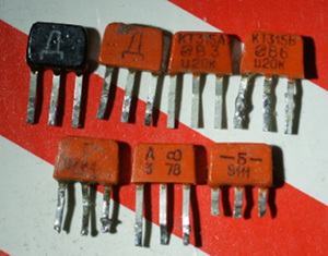
Here is a meeting I found:
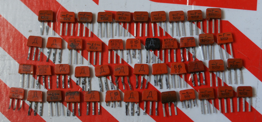
Those where the manufacturer’s sign is missing is the KT361, pnp option. The rest, with the logo - KT315 (even if the "letter in the center"). It is noteworthy that in times of a planned economy, fixed prices, and a formal lack of speculation - sometimes the price was written directly on transistors.
What is inside?
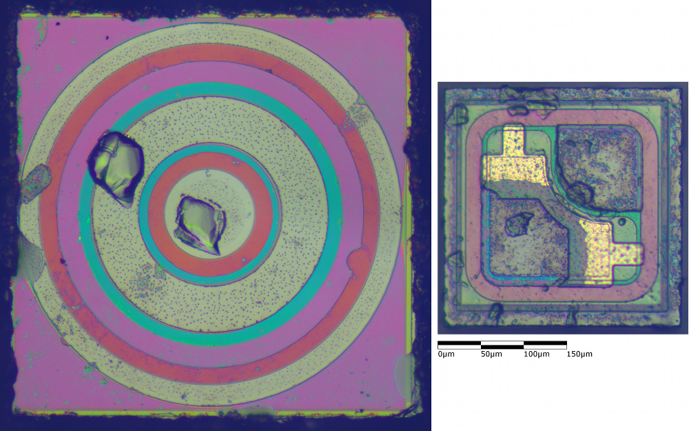
The oldest transistor I have found is the KT315A, released in March 1978.
We see that the crystal is broken off from the plate far from ideal, there is a lot of unused space around the transistor.
Here the crystal itself is the collector, in the center, if I am not mistaken, is the base circles, and around it there is a wider “belt” of the emitter. The base somehow dives under the emitter, and comes out from the back of the ring. Next, look at the KT315G, made in February 92nd, after 14 years of evolution. It is immediately evident that the place is spent much more economically, the crystal is cut off almost perfectly, small non-critical defects in photolithography are noticeable, apparently contact photolithography is still used here. However, for transistors this is quite enough.


And finally, KT361G, July 1984.

Comparison
If we compare the scale with the modern NXP BC847B transistor , we can see that it was possible to reduce the size by a factor of 2 again due to "rounding", but the transistor itself has not fundamentally changed - the same collector at the "bottom" of the crystal, and the wires of the emitter and base welded with wire.
It is noteworthy that with the BC847 the width / height of the crystal is almost equal to the thickness of the wafer; this is almost a silicon cube, not a wafer. It is difficult to reduce the area further, at least without further thinning the plate ( thinning of the plate is written correctly).
Future
Did KT315 die? Definitely not. Until now, it is, for example, in Integral 's price lists of 248 Belarusian rubles (~ 1 Russian ruble), i.e. probably still in production. Of course, with the development of automatic assembly of printed circuit boards, he had to give way to SMD options, for example, KT3129 and KT3130 and many others, including foreign counterparts BC846-BC848, BC856-BC858.
But in our memory he will remain forever :-)