An example of designing a digital device "on the fingers"
Hello, Habr! This is the beginning of a short series of two articles with a step-by-step design of a digital device with a focus on practice. Minimum “water” and maximum practice!

To get started, take the following output parameters: 0000110001110001
Note: there are many methods and programs for designing digital devices. Shown in the article may differ from the usual for you. This is normal.
The first step is to create a truth table according to the formula

where N is the number of possible options, and i is the number of output signals.
In the case presented, it will look like this:

Based on the data obtained, we can proceed to the construction of a truth table. For clarity, the input signals were designated as A, B, C and D, the output as F.
After building the truth table, you can begin to obtain SDNF. This is done in two steps:
As a result, there is such an SDNF:

Obtained SDNF must be reduced using Carnot cards.
Three steps to build Carnot maps:
The result is 4 groups:

The next step is to minimize the resulting groups. The general principle can be reduced to the following:
If 11 - the value does not change;
If 00 - negation is assigned;
If 01 (or 10) is crossed out.
The resulting works are linked into a disjunction:

After which the compiled expression is reduced to the basis of NAND using de Morgan's law (the negation of the conjunction is the disjunction of negatives, the negation of the disjunction is the conjunction of negations ):
Pay attention to the changes - a double negation has appeared (one per group) and one thing in common) and the signs have changed.
Optionally, you can also make a logical diagram. Why at will? Because further there will be a compilation of an electronic circuit based on logical elements, and it, in essence, is the same logical circuit, but with the ability to test performance.
Logic circuit example:
Basic calculations completed. Now you can postpone a piece of paper with a pen and a ruler. Go to the Electronics Workbench.
In this case, this stage acts as an “intermediate” and simplifies the process of transition from an expression in the basis of NAND to an electronic circuit based on microcircuits.

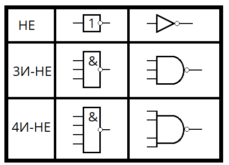
As you can see, the logical elements of the electronic circuit outwardly differ from those that were previously presented (in the logical circuit). This is due to the fact that in Electronics Workbench the graphic designation of logical elements is made according to ANSI standards, while the previously shown logic diagram was made in accordance with GOST 2.743-91.
Move on.
The performance of the electronic circuit is checked according to the truth table. To do this, you need to press the start button

and start switching, making a comparison with the truth table.
Example:

IMPORTANT: you need to check each line. A spot check will do nothing.
Based on the available data, an electronic circuit is built on the basis of microcircuits (it will also be possible to navigate using the obtained circuit during the design of the printed circuit board).
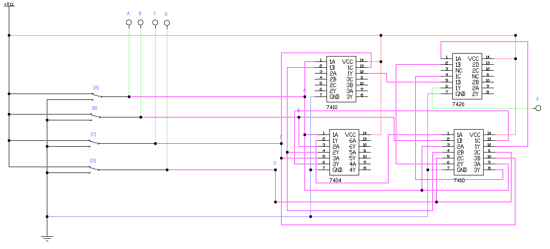
As you can see, in the obtained electronic circuit 4 microcircuits were used - 7404 (analog of K155LN1), 7410 (analog of K155LA4), 7410 (analog of K155LA4) and 7420 (analog of K155LA1). In order to understand how the connection occurs, you should refer to the actual image of the chips.
It may seem complicated at first, but over time you will realize that it is not so difficult.
IMPORTANT : do not forget to check.
To get started, take the following output parameters: 0000110001110001
Note: there are many methods and programs for designing digital devices. Shown in the article may differ from the usual for you. This is normal.
Tools, materials and more:
- Electronics Workbench
- Ruler, pen and leaflet (for general calculations)
- Basic knowledge of discrete mathematics, digital circuitry and the principle of operation of the presented programs
- Conventional graphic designation of chips 7404 (analog K155LN1), 7410 (analog K155LA4), 7410 (analog K155LA4) and 7420 (analog K155LA1)
- The actual image of chips 7404 (analogue K155LN1), 7410 (analogue K155LA4), 7410 (analogue K155LA4) and 7420 (analogue K155LA1)
Beginning of work
1. Construction of a truth table and finding the perfect disjunctive normal form (SDNF)
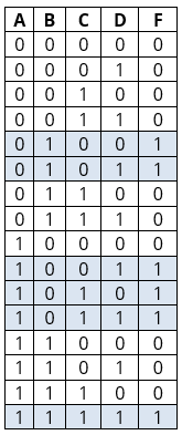
The first step is to create a truth table according to the formula
where N is the number of possible options, and i is the number of output signals.
In the case presented, it will look like this:
Based on the data obtained, we can proceed to the construction of a truth table. For clarity, the input signals were designated as A, B, C and D, the output as F.
After building the truth table, you can begin to obtain SDNF. This is done in two steps:
- The lines of the truth table in which F = 1 are highlighted.
- The conjunction of the variables for all selected lines is written out according to the following formula: if the value of the variable is 1, then the variable itself is included in the conjunction. If the value is 0, then the negation of the variable is turned on. The resulting conjunctions must be linked into a disjunction.
As a result, there is such an SDNF:
More clearly: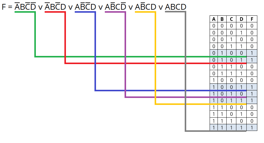
2. Creation of a Carnot map, minimization and reduction to the basis of NAND
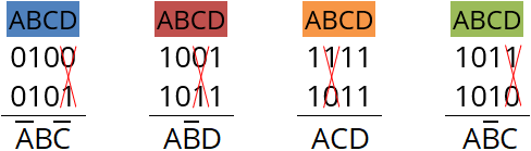
Obtained SDNF must be reduced using Carnot cards.
Three steps to build Carnot maps:
- since four variables are used (A, B, C and D), a table of 5 × 5 cells is constructed;
- the table is filled out on the basis of the “coordinates” from the truth table (from the lines in which F = 1) or the SDNF (the essence is one. It’s just who is more convenient)
- in conclusion, adjacent cells are combined into groups. Groups must not contain zeros. Groups must be a multiple of two. Groups may overlap.
The result is 4 groups:
More clearly:
The next step is to minimize the resulting groups. The general principle can be reduced to the following:
If 11 - the value does not change;
If 00 - negation is assigned;
If 01 (or 10) is crossed out.
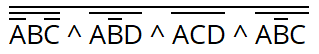
The resulting works are linked into a disjunction:
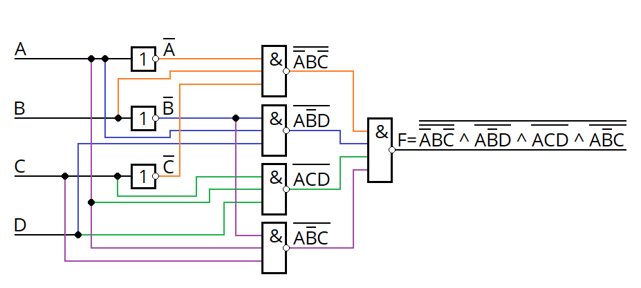
After which the compiled expression is reduced to the basis of NAND using de Morgan's law (the negation of the conjunction is the disjunction of negatives, the negation of the disjunction is the conjunction of negations ):
Pay attention to the changes - a double negation has appeared (one per group) and one thing in common) and the signs have changed.
Optionally, you can also make a logical diagram. Why at will? Because further there will be a compilation of an electronic circuit based on logical elements, and it, in essence, is the same logical circuit, but with the ability to test performance.
Logic circuit example:
3. Electronic circuit based on logic elements
Basic calculations completed. Now you can postpone a piece of paper with a pen and a ruler. Go to the Electronics Workbench.
In this case, this stage acts as an “intermediate” and simplifies the process of transition from an expression in the basis of NAND to an electronic circuit based on microcircuits.
More clearly: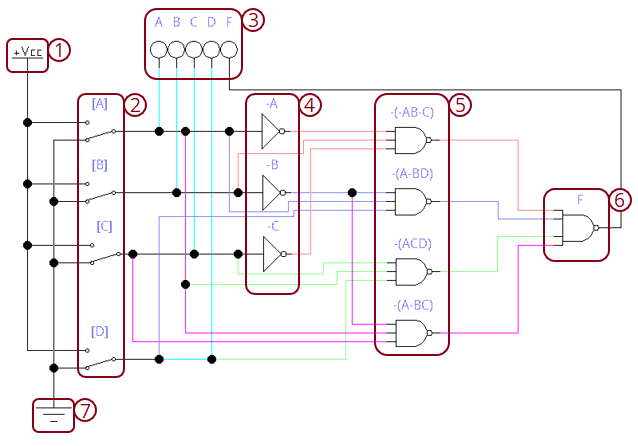
1 - Nutrition;
2 - Switches used for signaling;
3 - Indicators (used for visual verification of performance);
4 - Logical elements of the type "NOT";
5 - Logic elements of the type “3I-NOT”;
6 - A logical element of the type “4I-NOT”;
7 - Grounding.
1 - Nutrition;
2 - Switches used for signaling;
3 - Indicators (used for visual verification of performance);
4 - Logical elements of the type "NOT";
5 - Logic elements of the type “3I-NOT”;
6 - A logical element of the type “4I-NOT”;
7 - Grounding.
As you can see, the logical elements of the electronic circuit outwardly differ from those that were previously presented (in the logical circuit). This is due to the fact that in Electronics Workbench the graphic designation of logical elements is made according to ANSI standards, while the previously shown logic diagram was made in accordance with GOST 2.743-91.
Move on.
The performance of the electronic circuit is checked according to the truth table. To do this, you need to press the start button
and start switching, making a comparison with the truth table.
Example:
IMPORTANT: you need to check each line. A spot check will do nothing.
4. Chip-based electronic circuit
Based on the available data, an electronic circuit is built on the basis of microcircuits (it will also be possible to navigate using the obtained circuit during the design of the printed circuit board).
As you can see, in the obtained electronic circuit 4 microcircuits were used - 7404 (analog of K155LN1), 7410 (analog of K155LA4), 7410 (analog of K155LA4) and 7420 (analog of K155LA1). In order to understand how the connection occurs, you should refer to the actual image of the chips.
Actual Images:


It may seem complicated at first, but over time you will realize that it is not so difficult.
IMPORTANT : do not forget to check.