December 8, 2012 at 14:13
Shaking antiquity: interception of data flow between i386 and ATA controller using STM32
Good afternoon, dear Khabrovites. In today's article, we indulge in nostalgia, work with the good old iron, and try to tie in it no less good new. At the same time, let us recall how the ISA bus works and how the x86 processor communicates with peripherals in general.
A couple of days ago I was struck by my very first computer - the old man 386, on a processor from AMD (Am386-DX), with 4 megabytes of RAM, a VGA video card and a multi-card that takes on the functions of a drive controller, hard drive, parallel and serial ports.
Of course, he had long been spared from his case and from the ancient, dead hard - now he was just a motherboard with a pair of expansion cards. A few years ago I connected to it a newer hard drive, 10 GB (initially it had a disk of only 200 megabytes), on which I installed FreeDOS.
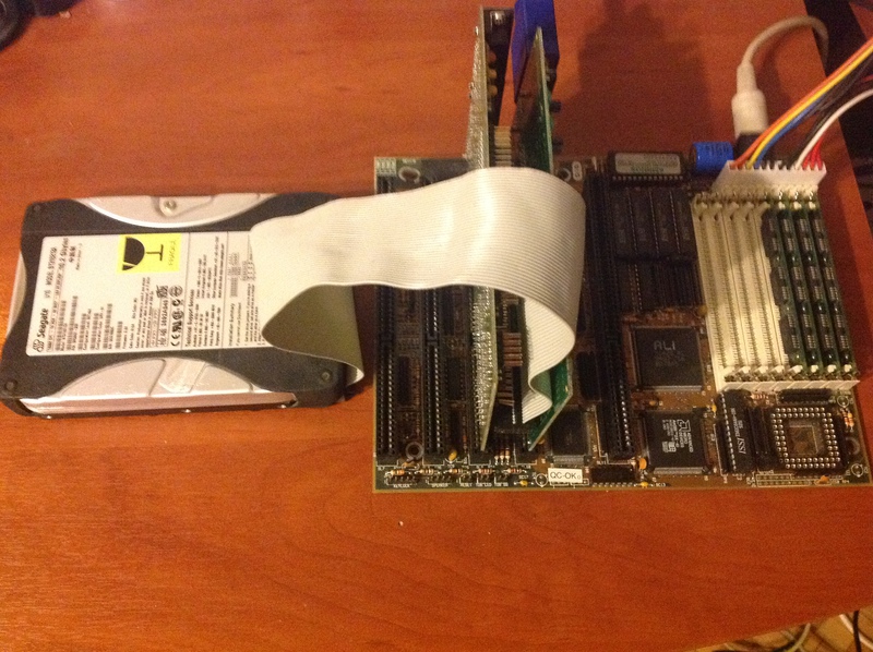
However, this time he refused to boot further than BIOS - judging by the sounds, 10 GB hard for several years of lying in the closet managed to go after two hundred meters.
And then I woke up to an acute desire to do something with this computer, to touch this antiquity, with which I began to get acquainted with IT, already as a developer, and not as a user. Ideally, I would certainly like to make a hard drive emulator that works with an SD card, but we will go towards this goal gradually. Let's start with a simpler task - we will assemble a device that hangs in parallel with a real hard disk controller, and logs data exchange in order to find out exactly how the old BIOS detects hard drives. Initially, I intended to do the same, but for the diskette controller, however, after my last hard die, all that I have left working is the BIOS, which does not check for floppy in any way. But he has a couple of items related to hard drives - the detection of hard drives and means for formatting them.
Of course, this is done very easily on FPGAs due to their architecture, but we will stick to the budget option and try to do this on the STM32F103 controller and several discrete logic circuits. So, let's begin.
Traditionally, we’ll go from the hardwood bottoms. Let's remember what exactly is the ISA bus that underlies old computers, and how to connect to it. For those who do not really understand the circuitry inside x86 machines, this will help shed light on the architecture of such systems. In fact, everything is very simple - in a “clean” ISA there are no Plug & Play tools - they appeared only in the next standard - and, therefore, no means of issuing an address to devices.
Thus, ISA-cards are devices with a hardware address (hard-wired circuitry, in the best case, with the ability to select a base address by jumpers). The bus itself contains 20 address lines, 16 data lines, several power signals, several IRQ lines, and a set of control signals.
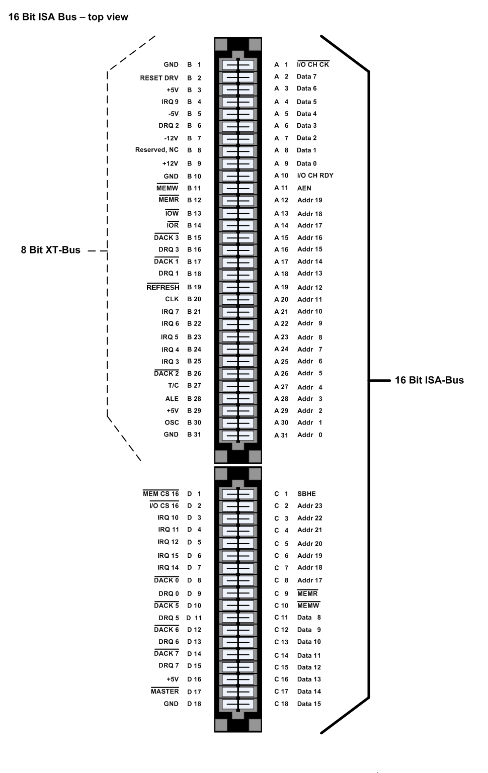
How does it all work? Suppose we need the ability to turn on / off several LEDs on our device. To do this, we will place a register chip on our ISA-board, for example, such as 74HC273 .
This is the most common 8-bit “latch” that remembers what it was fed to the input by signal. Connect the outputs of the register to the LEDs and forget about them. From a software point of view, interaction with a device on the ISA bus can be implemented in two ways.
In fact, behind the words “separate address space” lies a physically simple entity: there are 4 signals in the ISA bus - MEMW, MEMR, IOR, IOW . When executing a command to read / write to memory ( MOV ) or read / write to IO ( IN , OUT ), the desired address is set on the same bus, lines A0-A19 ISA. Data also goes along the same lines - D0-D15 . The only difference is that when reading from memory, the active level is set on the MEMR line , when writing to memory - MEMW , when reading from the IO port - IOR , when writing to it - IOW .
Thus, in order to make the simplest device with one register and LEDs, we need to determine when the address we need is set on the bus (we remember that no one gives us addresses, we must choose an address that will not conflict with existing peripherals), and on the IOW signal, enable the recording of data from lines D0-D8 in our register.
In more complex devices containing several registers, the senior address lines go to the decoder, forming an active output signal when they coincide with some "base" address of the device, while the younger ones form the register number to be addressed.
Let's move on to a more specific example - our ATA controller. For a better understanding of the principles of its work, I recommend that you read the articlefrom the OSDev wiki.
It is managed by nine IO registers, eight of which are arranged in a row, starting from the base address 0x1F0 . The ninth, unfortunately, is located at 0x3F6 , which somewhat complicates the decoding scheme.
Of course, we won’t get all the address lines on the controller and make a decoder on it, otherwise we won’t succeed - the clock frequency of the 8 MHz bus, the IO cycle, according to the specification, lasts 4 cycles, which gives us only 36 clock cycles at the frequency of 72 MHz for thought. Therefore, we will use cheap discrete logic chips.
If there wasn’t this ninth register that sticks out at 0x3F6 , then we would need to build a circuit that gives an active signal when on lines A9and A3 is set to zero, and on A4-A8 it is one (that is, for addresses 0x1F (..) ). Bits older than A9 in ISA cards usually do not decode, not paying attention to the possibility of access to the same device at the addresses located above.
The processing of the three least significant bits could already be entrusted to the controller. Alas, we still have an unreached register 0x3F6 .
The initial conditions (active lines A4-A8 and inactive A3 ) are always satisfied, since these bits are in the indicated states for both 0x1F (..) and 0x3F6 . A condition is added to them, which can be formulated as follows: with activeA9 - there should be active levels on A1 and A2 (address 0x3F6 )
That is,
Using the Logic.Ly online logic circuit simulator , I built this circuit based on the microcircuits I had - 74HC04, a quad element NOT , 74HC30 - an eight-input NAND and 74HC10, a triple three-input NAND .
Since we don’t have an OR element , we recall the rules of De Morgan - negation of a conjunction is a disjunction of negations and a negation of a disjunction is a conjunction of negations, or, in the form of logical equalities
We will use this:
We also do not have a pure AND , therefore, we will feed its components to the three-input NAND block and will enter the drop-off interrupt.
As you can see, all the logic fits exactly in three cases.
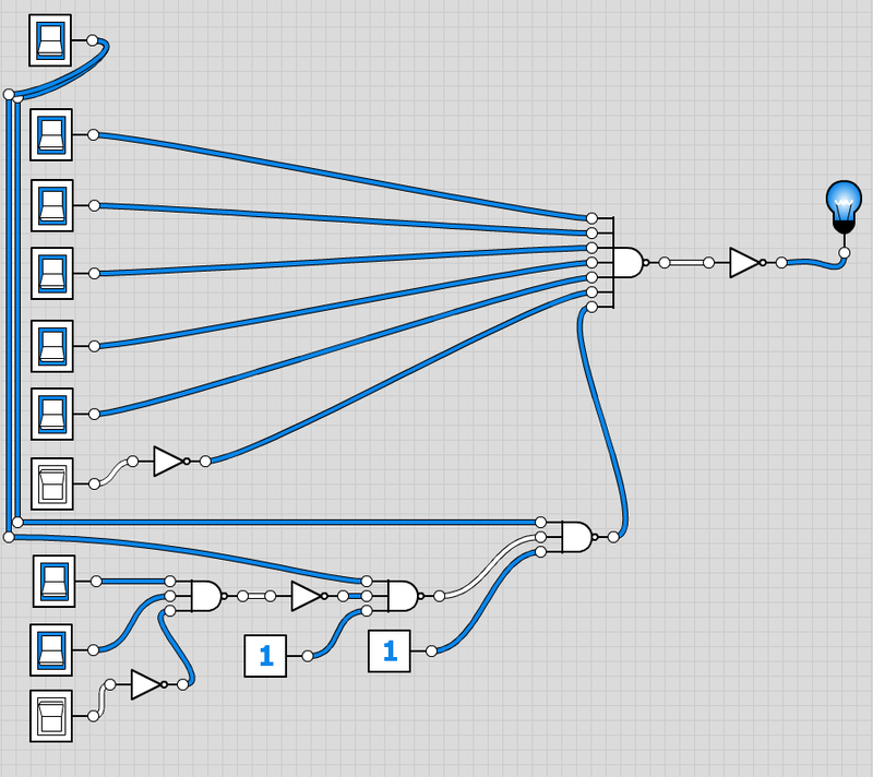
The presence of an active level on IOR or IOW is added to these conditions (do not forget that, according to the standard, the active level is low on them, that is, we have already inverted signals, ~ IOR and ~ IOW ):
The final scheme looks like this:
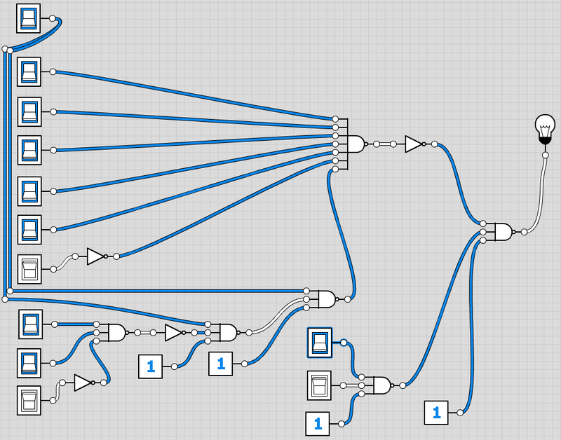
Now we begin to assemble it in iron, using the mock-up. First, we will arrange the first three microcircuits, to which the most input signals go, and take care of their connection to the power and ground buses.
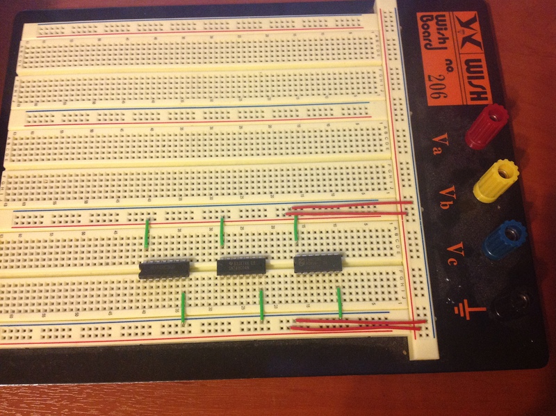
Carefully add the output circuits, then add the input ones in the form of sufficiently long probes, which we later plug into the computer motherboard:
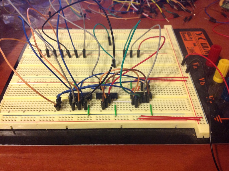
For convenience, I temporarily fixed the senior address inputs on the left ( A3-A9 ), the lower ones on the right ( A0-A2 ), and in the middle output signal CS2 .
Let's temporarily distract from the assembly and try to see with an oscilloscope what happened to us. So, we connect the address inputs to the bus - since ISA is exactly the bus, we do not need to try to stick the probes into the same slot where the ATA controller board is inserted, we choose any convenient one for us. The probes, unfortunately, were too small for such holes, so I also stuck a comb of straight pins on top - individually, the probes and pins drop out, but they stick together pretty well.
Also, do not forget to connect the ground and circuit power to the ISA, and at the same time - the ground of the oscilloscope probes.
We turn on the oscilloscope and the computer (I immediately went into the BIOS setup menu) and poked at the CLK signal . We should see something like this:
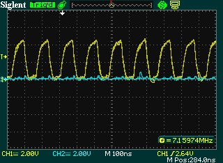
This, of course, is a bus clock whose frequency is usually 8 MHz. On my motherboard, its frequency is 7.19 MHz, which is reflected in the BIOS settings. Apparently, this is a feature of iron - BIOS did not allow me to lower this frequency, or at least set it to exactly 8 MHz, stubbornly setting 7.19 MHz. Anyway.
We check the contacts of the inputs of our circuit - by poking at any of them we will get a chaotic signal on the oscilloscope screen, since the system constantly accesses different addresses and ports. So if there is silence at the entrance, it means that you have lost contact, and you need to double-check it.
Now we are connected to our CS2 signal and observe the following picture:
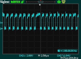
Quite expected - IOR and IOW signalsdo not participate in the formation of CS2 , so that it becomes active when the address on the bus coincides with the one specified by us ( 0x1F0-0x1F7 and 0x3F6 ). The system performs regular DRAM regeneration, so we get a beautiful periodic signal. Now is the time to adjust the sweep and levels of the oscilloscope to see the signals in all its glory.
After making sure that everything works, de-energize the circuit and finish it to the end, getting a hell of a mess of wires like this:
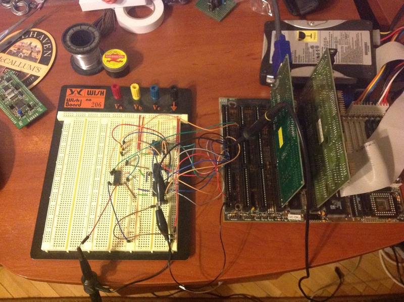
Turn on the computer again, go to the BIOS setup menu, turn on the oscilloscope.
No signals! Well, it's time to check the correctness of our calculations - select the item “Autodetect hard drive”. The first disk is detected quickly, and most likely, on the oscilloscope screen, we will not have time to notice anything unless we turn on single mode.
But the second disk (due to its absence) will be detected long enough for us to see this on the computer screen:
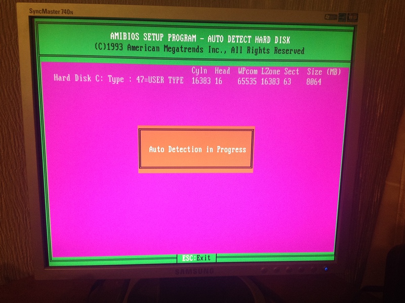
And on the oscilloscope screen - this:
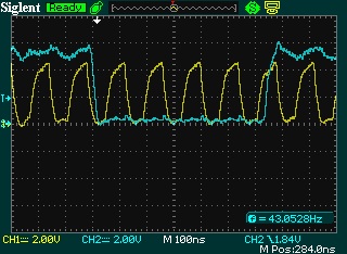
To completely verify our correctness, exit the disk detection, turn on the single mode oscilloscope and carefully watch nothing on his screen! No matter how much we wait, CSdoesn't get active! But just go into the disc detection, as we again catch a familiar picture, which is fully consistent with the standards - I / O cycles lasts four clock cycles.
Well, it's time to take the board with STM32 and connect it to the system!
I connected as follows: The
ISA data bus ( D0 - D7 ) is connected to GPIOD.0 - GPIOD.7 , the
three lowest address lines ( A0 - A2 ) to GPIOD.8 - GPIOD.10 ,
the address line A9 to GPIOD.11 (after all, we will need this bit to understand that the call goes not to 0x1F6 , but to 0x3F6 !) IOW
lines andIOR to GPIOD.12 and GPIOD.13 . CS
signal - to GPIOB.0 Now, when interrupting to GPIOB.0, we just need to read GPIOD-> IDR (Input Data Register), in which the lower 8 bits will be the desired data, the next four bits will be the address (moreover, the possible combinations are 0000 - 0111 and 1011 , corresponding to ports 0x1F0 - 0x1F7 and 0x3F6 ), the next two - by the mode (read at 01 or write at 10 ).
It is important to note the following - if we suddenly get a result with mode bits that are in an invalid state - 00 or 11 , this will signal us an error of operation - this fact will come in handy very soon.
So, we pass to a software.
With software, everything is extremely simple - we configure the GPIOD as an input, like GPIOB.0 , and then configure the drop interrupt on the EXTI line connected to GPIOB.0 .
In the interrupt handler, we will only read the value from the GPIOD and increment the pointer to the buffer. This buffer can then be sent to a computer for analysis via any interface, or not bother with it at all and see it directly in the debug.
The setup code is presented below:
And here is the interrupt handler code:
It's time to check what we did! We start the computer, go to the BIOS setup. Run the STMki debug. We go into the detection of disks, and, after the detection of drive C, we suspend the execution of the controller program. In the debug window, we see that some data has been caught, and there are a lot of them!
Then I did the following: from the debug window, I copied the contents of the buffer to MS Exel to split into columns and get rid of the first one containing the variable name, after which I copied the column with the values to a new text file, and got something like this:
Now it's time to write a program to process the results in any convenient language, I used C # for this. We need to break each input uint into data, address and access mode, creating a readable report. This is done very simply, with the usual bit shifts and bitwise operations, for example, like this:
However, we’ll run the program, I encountered a big problem - many records from the file contained access mode 11 , which meant there were no read / write signals. Since the entrance to the interrap was possible only with one of these signals, I concluded that the interrap lasts longer than the bus cycle, and I just do not have time to read the valid data.
To test this hypothesis, I decided to set the pin GPIOB.2 to 1 at the entrance to the interrupt, and reset it to 0 at the exit, after which I hung the oscilloscope probe on it.
The result was depressing:
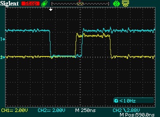
As you can see, the system enters the interrap at the very end of the I / O cycle, despite the promised 12 clock cycles for input. Not even an attribute helped(naked) , the difference was completely negligible.
This upset me, but I decided to try to overclock the controller - the same AVRs were very good at overclocking, why not check how STM32 is doing with this. To do this, we need to go to the system_stm32f10x.c file , to the procedure for initializing the system clock SetSysClockTo72 , and find the line
In this line, you should change the constant RCC_CFGR_PLLMULL9 to something more. I will say right away - I tried all the options and eventually settled on the maximum value, RCC_CFGR_PLLMULL16 . Thus, the controller wound up quite calmly at a frequency of 128 MHz instead of 72, without even basking.
By the way, it would be very good to bind the controller clock signal to the ISA bus CLK in order to work with it synchronously, but I really did not want to solder the quartz on the debug board, so I did not do this.
Let's see what the oscilloscope gives out now:
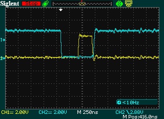
Finally, we began to enter the interrupt early enough to have time to process it! Let's get the input data again and try to analyze it.
I added some more to the program so that the report would be formatted and immediately with the names of the registers being accessed. In the case of the wrong access mode, a line about the invalid data is added to the report.
Here is the result of the program:
As we see, there are no more invalid data.
Let's try to figure out how BIOS conducts detection.
In the beginning, he persistently writes and reads into registers that specify the address - making sure that the same value that was written is read out. If the ATA controller is not in the system, the BIOS will try to write-read this register for a long time, 0x1F4 - this is an example of a report with the controller board pulled out:
Then it sends a 0x10 command , the value of which was kindly prompted by mark_ablov and which is an outdated recalibration command that forces the disk to rearrange its magnetic heads to sector 0. After that, the BIOS checks the status byte, waiting for the command to complete (you can see that the hard drive does not even enter the BUSY state , immediately responding that he completed).
And finally - the command 0xEC , DRIVE IDENTIFY , in response to which the hard gives 256 16-bit words of disk information.
Before starting to read them from port 0x1F0 , the BIOS requests a status byte from register 0x1F7 , waiting for the disk to be ready.
Here, unfortunately, I realized my mistake - I decided that the data is issued in 8 bits, since the control registers are 8-bit. However, as it turned out, the data is output in 16 bits, so I received only 256 low bytes. To get the full information, you will have to redo the scheme a bit, giving the entire GPIOD to the data, and display the address and access mode to other pins, which, of course, will increase the delay in processing them.
Therefore, at the moment I have stopped, although perhaps in the near future I will continue to work and try to sit on the bus not as a monitor, but as a device. ISA bus has wonderful IOCHRDY signalBy setting the inactive level at which, the device signals the need to increase the duration of the IO cycle, which means that perhaps I have enough time to switch the pins to the output and issue my status.
That's all for now, thanks for watching.
Upd :
Just discovered an interesting thing. If in the project settings you set optimization O1 instead of O3, then the time to enter the interrap is exactly what it should be. After some research, I found out that when O2 or O3 optimization is turned on, the compiler rearranges the instructions, because of which the signal pin is set to 1 not immediately after entering the interrap, but after part of the code has been executed.
Thus, when O1 is optimized on an oscilloscope, it is clear that the system entered the interrupt processor earlier, but the execution time of this processor is longer than in the case of O3.
Introduction
A couple of days ago I was struck by my very first computer - the old man 386, on a processor from AMD (Am386-DX), with 4 megabytes of RAM, a VGA video card and a multi-card that takes on the functions of a drive controller, hard drive, parallel and serial ports.
Of course, he had long been spared from his case and from the ancient, dead hard - now he was just a motherboard with a pair of expansion cards. A few years ago I connected to it a newer hard drive, 10 GB (initially it had a disk of only 200 megabytes), on which I installed FreeDOS.
However, this time he refused to boot further than BIOS - judging by the sounds, 10 GB hard for several years of lying in the closet managed to go after two hundred meters.
And then I woke up to an acute desire to do something with this computer, to touch this antiquity, with which I began to get acquainted with IT, already as a developer, and not as a user. Ideally, I would certainly like to make a hard drive emulator that works with an SD card, but we will go towards this goal gradually. Let's start with a simpler task - we will assemble a device that hangs in parallel with a real hard disk controller, and logs data exchange in order to find out exactly how the old BIOS detects hard drives. Initially, I intended to do the same, but for the diskette controller, however, after my last hard die, all that I have left working is the BIOS, which does not check for floppy in any way. But he has a couple of items related to hard drives - the detection of hard drives and means for formatting them.
Of course, this is done very easily on FPGAs due to their architecture, but we will stick to the budget option and try to do this on the STM32F103 controller and several discrete logic circuits. So, let's begin.
Iron
Traditionally, we’ll go from the hardwood bottoms. Let's remember what exactly is the ISA bus that underlies old computers, and how to connect to it. For those who do not really understand the circuitry inside x86 machines, this will help shed light on the architecture of such systems. In fact, everything is very simple - in a “clean” ISA there are no Plug & Play tools - they appeared only in the next standard - and, therefore, no means of issuing an address to devices.
Thus, ISA-cards are devices with a hardware address (hard-wired circuitry, in the best case, with the ability to select a base address by jumpers). The bus itself contains 20 address lines, 16 data lines, several power signals, several IRQ lines, and a set of control signals.
How does it all work? Suppose we need the ability to turn on / off several LEDs on our device. To do this, we will place a register chip on our ISA-board, for example, such as 74HC273 .
This is the most common 8-bit “latch” that remembers what it was fed to the input by signal. Connect the outputs of the register to the LEDs and forget about them. From a software point of view, interaction with a device on the ISA bus can be implemented in two ways.
- With the help of memory mapping - then we will decode the read / write signals of the memory and output the results to the bus instead of the DRAM controller - this is how the video card does, its video memory is mapped to the address space of the computer's memory. Thus, writing to the memory of a video card for a computer is no different from writing to its RAM and is performed by the usual MOV command .
- For those devices where it is not required to transfer large blocks of data, the so-called “I / O space” is used - a separate address space allocated for peripheral devices and limited to 16 address bits. It is accessed by the IN and OUT commands (read and write to I / O ports)
In fact, behind the words “separate address space” lies a physically simple entity: there are 4 signals in the ISA bus - MEMW, MEMR, IOR, IOW . When executing a command to read / write to memory ( MOV ) or read / write to IO ( IN , OUT ), the desired address is set on the same bus, lines A0-A19 ISA. Data also goes along the same lines - D0-D15 . The only difference is that when reading from memory, the active level is set on the MEMR line , when writing to memory - MEMW , when reading from the IO port - IOR , when writing to it - IOW .
Thus, in order to make the simplest device with one register and LEDs, we need to determine when the address we need is set on the bus (we remember that no one gives us addresses, we must choose an address that will not conflict with existing peripherals), and on the IOW signal, enable the recording of data from lines D0-D8 in our register.
In more complex devices containing several registers, the senior address lines go to the decoder, forming an active output signal when they coincide with some "base" address of the device, while the younger ones form the register number to be addressed.
Let's move on to a more specific example - our ATA controller. For a better understanding of the principles of its work, I recommend that you read the articlefrom the OSDev wiki.
It is managed by nine IO registers, eight of which are arranged in a row, starting from the base address 0x1F0 . The ninth, unfortunately, is located at 0x3F6 , which somewhat complicates the decoding scheme.
Of course, we won’t get all the address lines on the controller and make a decoder on it, otherwise we won’t succeed - the clock frequency of the 8 MHz bus, the IO cycle, according to the specification, lasts 4 cycles, which gives us only 36 clock cycles at the frequency of 72 MHz for thought. Therefore, we will use cheap discrete logic chips.
If there wasn’t this ninth register that sticks out at 0x3F6 , then we would need to build a circuit that gives an active signal when on lines A9and A3 is set to zero, and on A4-A8 it is one (that is, for addresses 0x1F (..) ). Bits older than A9 in ISA cards usually do not decode, not paying attention to the possibility of access to the same device at the addresses located above.
The processing of the three least significant bits could already be entrusted to the controller. Alas, we still have an unreached register 0x3F6 .
The initial conditions (active lines A4-A8 and inactive A3 ) are always satisfied, since these bits are in the indicated states for both 0x1F (..) and 0x3F6 . A condition is added to them, which can be formulated as follows: with activeA9 - there should be active levels on A1 and A2 (address 0x3F6 )
That is,
CS0 = A8 & A7 & A6 & A5 & A4 & ~A3
CS1 = A1 & A2 & A9
CS2 = CS0 & (~A9 | CS1)
Using the Logic.Ly online logic circuit simulator , I built this circuit based on the microcircuits I had - 74HC04, a quad element NOT , 74HC30 - an eight-input NAND and 74HC10, a triple three-input NAND .
Since we don’t have an OR element , we recall the rules of De Morgan - negation of a conjunction is a disjunction of negations and a negation of a disjunction is a conjunction of negations, or, in the form of logical equalities
~(A&B) = ~A | ~B
~(A|B) = ~A & ~B
We will use this:
 ~( ~ (~A9 | CS1))) = ~(A9&~CS1) - = (A9 NAND ~CS1)
CS2 = CS0 & (A9 NAND ~CS1)
We also do not have a pure AND , therefore, we will feed its components to the three-input NAND block and will enter the drop-off interrupt.
As you can see, all the logic fits exactly in three cases.
The presence of an active level on IOR or IOW is added to these conditions (do not forget that, according to the standard, the active level is low on them, that is, we have already inverted signals, ~ IOR and ~ IOW ):
CS = CS2 & (IOR | IOW)
(IOR|IOW) = ~(~(IOR & IOW) ) = ~(~IOR & ~ IOW) = (IOR NAND IOW)
CS = CS2 & (IOR NAND IOW)
The final scheme looks like this:
Now we begin to assemble it in iron, using the mock-up. First, we will arrange the first three microcircuits, to which the most input signals go, and take care of their connection to the power and ground buses.
Carefully add the output circuits, then add the input ones in the form of sufficiently long probes, which we later plug into the computer motherboard:
For convenience, I temporarily fixed the senior address inputs on the left ( A3-A9 ), the lower ones on the right ( A0-A2 ), and in the middle output signal CS2 .
Let's temporarily distract from the assembly and try to see with an oscilloscope what happened to us. So, we connect the address inputs to the bus - since ISA is exactly the bus, we do not need to try to stick the probes into the same slot where the ATA controller board is inserted, we choose any convenient one for us. The probes, unfortunately, were too small for such holes, so I also stuck a comb of straight pins on top - individually, the probes and pins drop out, but they stick together pretty well.
Also, do not forget to connect the ground and circuit power to the ISA, and at the same time - the ground of the oscilloscope probes.
We turn on the oscilloscope and the computer (I immediately went into the BIOS setup menu) and poked at the CLK signal . We should see something like this:
This, of course, is a bus clock whose frequency is usually 8 MHz. On my motherboard, its frequency is 7.19 MHz, which is reflected in the BIOS settings. Apparently, this is a feature of iron - BIOS did not allow me to lower this frequency, or at least set it to exactly 8 MHz, stubbornly setting 7.19 MHz. Anyway.
We check the contacts of the inputs of our circuit - by poking at any of them we will get a chaotic signal on the oscilloscope screen, since the system constantly accesses different addresses and ports. So if there is silence at the entrance, it means that you have lost contact, and you need to double-check it.
Now we are connected to our CS2 signal and observe the following picture:
Quite expected - IOR and IOW signalsdo not participate in the formation of CS2 , so that it becomes active when the address on the bus coincides with the one specified by us ( 0x1F0-0x1F7 and 0x3F6 ). The system performs regular DRAM regeneration, so we get a beautiful periodic signal. Now is the time to adjust the sweep and levels of the oscilloscope to see the signals in all its glory.
After making sure that everything works, de-energize the circuit and finish it to the end, getting a hell of a mess of wires like this:
Turn on the computer again, go to the BIOS setup menu, turn on the oscilloscope.
No signals! Well, it's time to check the correctness of our calculations - select the item “Autodetect hard drive”. The first disk is detected quickly, and most likely, on the oscilloscope screen, we will not have time to notice anything unless we turn on single mode.
But the second disk (due to its absence) will be detected long enough for us to see this on the computer screen:
And on the oscilloscope screen - this:
To completely verify our correctness, exit the disk detection, turn on the single mode oscilloscope and carefully watch nothing on his screen! No matter how much we wait, CSdoesn't get active! But just go into the disc detection, as we again catch a familiar picture, which is fully consistent with the standards - I / O cycles lasts four clock cycles.
Well, it's time to take the board with STM32 and connect it to the system!
I connected as follows: The
ISA data bus ( D0 - D7 ) is connected to GPIOD.0 - GPIOD.7 , the
three lowest address lines ( A0 - A2 ) to GPIOD.8 - GPIOD.10 ,
the address line A9 to GPIOD.11 (after all, we will need this bit to understand that the call goes not to 0x1F6 , but to 0x3F6 !) IOW
lines andIOR to GPIOD.12 and GPIOD.13 . CS
signal - to GPIOB.0 Now, when interrupting to GPIOB.0, we just need to read GPIOD-> IDR (Input Data Register), in which the lower 8 bits will be the desired data, the next four bits will be the address (moreover, the possible combinations are 0000 - 0111 and 1011 , corresponding to ports 0x1F0 - 0x1F7 and 0x3F6 ), the next two - by the mode (read at 01 or write at 10 ).
It is important to note the following - if we suddenly get a result with mode bits that are in an invalid state - 00 or 11 , this will signal us an error of operation - this fact will come in handy very soon.
So, we pass to a software.
Software
With software, everything is extremely simple - we configure the GPIOD as an input, like GPIOB.0 , and then configure the drop interrupt on the EXTI line connected to GPIOB.0 .
In the interrupt handler, we will only read the value from the GPIOD and increment the pointer to the buffer. This buffer can then be sent to a computer for analysis via any interface, or not bother with it at all and see it directly in the debug.
The setup code is presented below:
GPIO_InitTypeDef GPIO_InitStructure;
EXTI_InitTypeDef EXTI_InitStructure;
 RCC_APB2PeriphClockCmd(RCC_APB2Periph_GPIOD|RCC_APB2Periph_GPIOB|RCC_APB2Periph_AFIO, ENABLE);
    GPIO_InitStructure.GPIO_Speed = GPIO_Speed_50MHz;
    GPIO_InitStructure.GPIO_Mode = GPIO_Mode_IPD;
    GPIO_InitStructure.GPIO_Pin = GPIO_Pin_0|GPIO_Pin_1|GPIO_Pin_2|GPIO_Pin_3|
    								GPIO_Pin_4|GPIO_Pin_5|GPIO_Pin_6|GPIO_Pin_7
    								|GPIO_Pin_8|GPIO_Pin_9|GPIO_Pin_10|GPIO_Pin_11|
    								 GPIO_Pin_12|GPIO_Pin_13;
    GPIO_Init(GPIOD, &GPIO_InitStructure);
    GPIO_InitStructure.GPIO_Mode = GPIO_Mode_IPU;
    GPIO_InitStructure.GPIO_Pin = GPIO_Pin_0;
    GPIO_Init(GPIOB, &GPIO_InitStructure);
    GPIO_InitStructure.GPIO_Mode = GPIO_Mode_Out_PP;
    GPIO_InitStructure.GPIO_Pin = GPIO_Pin_2;
    GPIO_Init(GPIOB, &GPIO_InitStructure);
    GPIO_EXTILineConfig(GPIO_PortSourceGPIOB, GPIO_PinSource0);
    EXTI_InitStructure.EXTI_Line = EXTI_Line0;
    EXTI_InitStructure.EXTI_Mode = EXTI_Mode_Interrupt;
    EXTI_InitStructure.EXTI_Trigger = EXTI_Trigger_Falling;
    EXTI_InitStructure.EXTI_LineCmd = ENABLE;
    EXTI_Init(&EXTI_InitStructure);
    NVIC_InitTypeDef NVIC_InitStructure;
    NVIC_SetVectorTable(NVIC_VectTab_FLASH, 0x0);
    NVIC_PriorityGroupConfig(NVIC_PriorityGroup_0);
    NVIC_InitStructure.NVIC_IRQChannel = EXTI0_IRQn;
    NVIC_InitStructure.NVIC_IRQChannelPreemptionPriority = 0;
    NVIC_InitStructure.NVIC_IRQChannelSubPriority = 0;
    NVIC_InitStructure.NVIC_IRQChannelCmd = ENABLE;
    NVIC_Init(&NVIC_InitStructure);
And here is the interrupt handler code:
uint16_t Log[1024];
uint16_t ptr=0;
void EXTI0_IRQHandler()
{
	Log[ptr]=GPIOD->IDR;
	ptr++;
	EXTI_ClearITPendingBit(EXTI_Line0);
}
Tests, debugging and finishing
It's time to check what we did! We start the computer, go to the BIOS setup. Run the STMki debug. We go into the detection of disks, and, after the detection of drive C, we suspend the execution of the controller program. In the debug window, we see that some data has been caught, and there are a lot of them!
Then I did the following: from the debug window, I copied the contents of the buffer to MS Exel to split into columns and get rid of the first one containing the variable name, after which I copied the column with the values to a new text file, and got something like this:
58453
54527
42069
38143
42069
38143
...
Now it's time to write a program to process the results in any convenient language, I used C # for this. We need to break each input uint into data, address and access mode, creating a readable report. This is done very simply, with the usual bit shifts and bitwise operations, for example, like this:
var busData = uint.Parse(entry);
uint data = (busData & 0xFF);
uint address = ((busData & 0xFF00) >> 8);
uint rw = (address & 0x30)>>4;
address = (address & 0x0F);
However, we’ll run the program, I encountered a big problem - many records from the file contained access mode 11 , which meant there were no read / write signals. Since the entrance to the interrap was possible only with one of these signals, I concluded that the interrap lasts longer than the bus cycle, and I just do not have time to read the valid data.
To test this hypothesis, I decided to set the pin GPIOB.2 to 1 at the entrance to the interrupt, and reset it to 0 at the exit, after which I hung the oscilloscope probe on it.
The result was depressing:
As you can see, the system enters the interrap at the very end of the I / O cycle, despite the promised 12 clock cycles for input. Not even an attribute helped(naked) , the difference was completely negligible.
This upset me, but I decided to try to overclock the controller - the same AVRs were very good at overclocking, why not check how STM32 is doing with this. To do this, we need to go to the system_stm32f10x.c file , to the procedure for initializing the system clock SetSysClockTo72 , and find the line
RCC->CFGR |= (uint32_t)(RCC_CFGR_PLLSRC_HSE | RCC_CFGR_PLLMULL9);
In this line, you should change the constant RCC_CFGR_PLLMULL9 to something more. I will say right away - I tried all the options and eventually settled on the maximum value, RCC_CFGR_PLLMULL16 . Thus, the controller wound up quite calmly at a frequency of 128 MHz instead of 72, without even basking.
By the way, it would be very good to bind the controller clock signal to the ISA bus CLK in order to work with it synchronously, but I really did not want to solder the quartz on the debug board, so I did not do this.
Let's see what the oscilloscope gives out now:
Finally, we began to enter the interrupt early enough to have time to process it! Let's get the input data again and try to analyze it.
I added some more to the program so that the report would be formatted and immediately with the names of the registers being accessed. In the case of the wrong access mode, a line about the invalid data is added to the report.
Here is the result of the program:
WRITE:	Cylinder Low	[0x1F4]		VALUE:	0x55
READ:	Cylinder Low	[0x1F4]		VALUE:	0x55
WRITE:	Cylinder Low	[0x1F4]		VALUE:	0xAA
READ:	Cylinder Low	[0x1F4]		VALUE:	0xAA
WRITE:	Cylinder Low	[0x1F4]		VALUE:	0x0F
READ:	Cylinder Low	[0x1F4]		VALUE:	0x0F
WRITE:	Cylinder Low	[0x1F4]		VALUE:	0x00
READ:	Cylinder Low	[0x1F4]		VALUE:	0x00
READ:	Status		[0x1F7]		VALUE:	0x50
WRITE:	Drive/Head	[0x1F6]		VALUE:	0xA0
READ:	Status		[0x1F7]		VALUE:	0x50
WRITE:	Drive/Head	[0x1F6]		VALUE:	0x04
WRITE:	Drive/Head	[0x1F6]		VALUE:	0x00
READ:	Status		[0x1F7]		VALUE:	0x50
WRITE:	Drive/Head	[0x1F6]		VALUE:	0xA0
READ:	Status		[0x1F7]		VALUE:	0x50
WRITE:	Drive/Head	[0x1F6]		VALUE:	0xA0
READ:	Status		[0x1F7]		VALUE:	0x50
WRITE:	Command		[0x1F7]		VALUE:	0x10
READ:	Status		[0x1F7]		VALUE:	0x50
READ:	Status		[0x1F7]		VALUE:	0x50
WRITE:	Drive/Head	[0x1F6]		VALUE:	0xA0
READ:	Status		[0x1F7]		VALUE:	0x50
WRITE:	Drive/Head	[0x1F6]		VALUE:	0xA0
READ:	Status		[0x1F7]		VALUE:	0x50
WRITE:	Command		[0x1F7]		VALUE:	0xEC
READ:	Status		[0x1F7]		VALUE:	0x58
READ:	Data		[0x1F0]		VALUE:	0x5A
READ:	Data		[0x1F0]		VALUE:	0xFF
READ:	Data		[0x1F0]		VALUE:	0x00
READ:	Data		[0x1F0]		VALUE:	0x10
READ:	Data		[0x1F0]		VALUE:	0x00
READ:	Data		[0x1F0]		VALUE:	0x00
READ:	Data		[0x1F0]		VALUE:	0x3F
READ:	Data		[0x1F0]		VALUE:	0x00
READ:	Data		[0x1F0]		VALUE:	0x00
READ:	Data		[0x1F0]		VALUE:	0x00
READ:	Data		[0x1F0]		VALUE:	0x45
...
As we see, there are no more invalid data.
Let's try to figure out how BIOS conducts detection.
In the beginning, he persistently writes and reads into registers that specify the address - making sure that the same value that was written is read out. If the ATA controller is not in the system, the BIOS will try to write-read this register for a long time, 0x1F4 - this is an example of a report with the controller board pulled out:
WRITE:	Cylinder Low	[0x1F4]	VALUE:	0x55
READ:	Cylinder Low	[0x1F4]	VALUE:	0xFF
WRITE:	Cylinder Low	[0x1F4]	VALUE:	0x55
READ:	Cylinder Low	[0x1F4]	VALUE:	0xFF
...
WRITE:	Cylinder Low	[0x1F4]	VALUE:	0x55
READ:	Cylinder Low	[0x1F4]	VALUE:	0xFF
WRITE:	Cylinder Low	[0x1F4]	VALUE:	0x55
Then it sends a 0x10 command , the value of which was kindly prompted by mark_ablov and which is an outdated recalibration command that forces the disk to rearrange its magnetic heads to sector 0. After that, the BIOS checks the status byte, waiting for the command to complete (you can see that the hard drive does not even enter the BUSY state , immediately responding that he completed).
And finally - the command 0xEC , DRIVE IDENTIFY , in response to which the hard gives 256 16-bit words of disk information.
Before starting to read them from port 0x1F0 , the BIOS requests a status byte from register 0x1F7 , waiting for the disk to be ready.
Here, unfortunately, I realized my mistake - I decided that the data is issued in 8 bits, since the control registers are 8-bit. However, as it turned out, the data is output in 16 bits, so I received only 256 low bytes. To get the full information, you will have to redo the scheme a bit, giving the entire GPIOD to the data, and display the address and access mode to other pins, which, of course, will increase the delay in processing them.
Therefore, at the moment I have stopped, although perhaps in the near future I will continue to work and try to sit on the bus not as a monitor, but as a device. ISA bus has wonderful IOCHRDY signalBy setting the inactive level at which, the device signals the need to increase the duration of the IO cycle, which means that perhaps I have enough time to switch the pins to the output and issue my status.
That's all for now, thanks for watching.
Upd :
Just discovered an interesting thing. If in the project settings you set optimization O1 instead of O3, then the time to enter the interrap is exactly what it should be. After some research, I found out that when O2 or O3 optimization is turned on, the compiler rearranges the instructions, because of which the signal pin is set to 1 not immediately after entering the interrap, but after part of the code has been executed.
Thus, when O1 is optimized on an oscilloscope, it is clear that the system entered the interrupt processor earlier, but the execution time of this processor is longer than in the case of O3.