How to compress bootloader for STM8 to 18 bytes in FLASH memory
In the process of searching for the bootloader for the STM8S103F3 microcontroller, it was found that the existing bootloaders are mostly written in “C”, “steal” a significant amount of FLASH memory, transfer the interrupt vector table.
The loader was necessary for some device to which it is impossible to connect the programmer.
It was decided to try to write the bootloader on its own with the following requirements:
- the bootloader should be called STM8uLoader;
- the code should be written in assembler (since assembler is not legally prohibited by law);
- the loader should occupy the minimum possible amount in FLASH memory, the volume occupied in the computer will be considered unlimited;
- the loader should not move the table of interrupt vectors;
- the bootloader must have the minimum functionality, the entire main functionality must be assumed by the computer;
- the loader must transfer control to the application program within a reasonable time after resetting / turning on when there is no connection with the computer.
The first condition was instantly fulfilled , but over subsequent requirements had to work.
To save the vector table in its place, it was decided to place the code at the end of the FLASH memory and switch to it immediately from the reset vector $ 8000.
When loading, control is transferred to the loader code at $ 9FC2. The loader configures the UART 9600 8N1, waits for two bytes on the UART, and without waiting for it passes control to the application program at the address stored in the $ 9FFE pair: $ 9FFF.
If the bootloader accepts the high and low bytes of the size of the expected dump from the host program, then takes the dump itself, puts the dump in the RAM memory and transfers control to it.
Further, all care falls on the program in the computer and the dump sent by it. It should send exactly those dumps that are needed to perform the current task (reading / erasing / writing / copying STM8 memory cells). Dumps should be able to replace each other in RAM memory and transfer control to the application program.
The address of the transition to the application program here is $ 9FFE: $ 9FFF.
Selecting 65 bytes from the FLASH memory (in STM8S103F3, its total is 8192 bytes) is not human. After all, the unused EEPROM memory with its 640 bytes is lying around. Let's divide the bootloader code into two parts, boot_FLASH and boot_EEPROM.
When loading, control of the boot_FLASH code is transferred to the address $ 9FEF. boot_FLASH copies the boot_EEPROM code image from EEPROM memory into RAM memory and transfers control to it.
Now the boot_EEPROM configures the UART 9600 8N1, waits for UART bytes, and without waiting for it transfers control to the application program (the address is $ 9FFE: $ 9FFF).
If the boot_EEPROM accepts a byte with the size of the expected dump for RAM memory, then takes a dump, dumps it to another area of RAM memory and transfers control to it.
Then everything is like in the first stage.
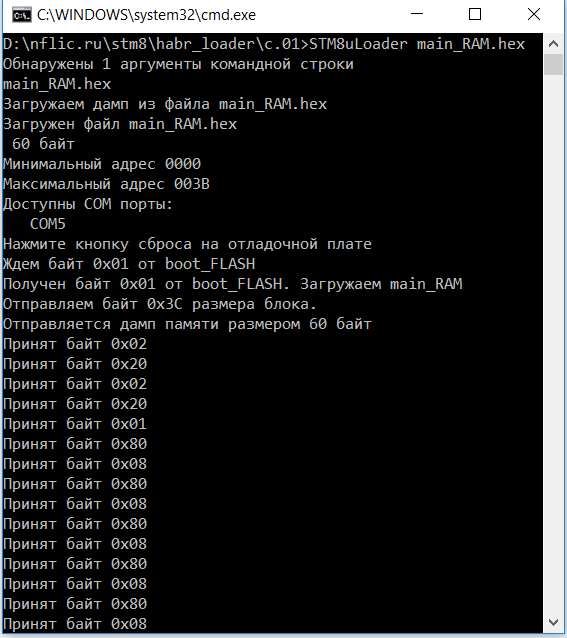
Run the file runSTM8uLoader.bat , press the reset button on the board, the loader sends byte 0x01. A memory dump with the code from the main_RAM.hex file is sent to the STM8 RAM memory. The board starts blinking the LED and sending bytes 0x20 and 0x02. Press the reset button again. The application program starts from FLASH memory, the LED starts blinking faster and sending bytes 0x80 and 0x08.
With the EEPROM memory, of course, we hurried. Where now to store the sinuses and other tables? Yes, and with FLASH memory is not all clear. Who decided to store the transfer address of the control application program in memory FLASH? And the same byte of the bootloader version is generally stored in two places at once. Where to squeeze in 52 bytes intended for EEPROM?
Here we can help lithography. EEPROM memory consists of 10 blocks of 64 bytes each. To add one more block to these blocks, but with a different size is not economically feasible. STMicroelectronics did just that, added another block of 64 bytes in size, called this area OPTION Bytes and stores there the important non-volatile settings of the microcontroller (in STM8S103F3 it is as much as 11 bytes). And of course, STM has forgotten to mention that there are still 53 workable cells in this area. Apparently there are a lot of STM8 models, you need to leave room for future important settings.
Our loader claims only for STM8 models without built-in loaders. For this, we are taking backup cells of the OPTION Bytes block while nobody sees it. The truth is there is one small, but solvableinconvenience. Normal programmer will not allow you to write information in these cells.
When loading, control of the initial copier boot_FLASH is transferred to the address $ 9FF2. boot_FLASH transfers the boot_OPTION bootloader image from the OPTION Bytes area to the RAM memory.
boot_OPTION configures the UART 9600 8N1, sends the UART bytes with its version, waits for the UART bytes from the host program, and without waiting for 0.2 seconds, transfers control to the application program at the address located in the pair $ 4831: $ 4832.
If, after sending a byte with its version, the boot_OPTION accepts a byte of the size of the expected dump, then the dump follows, dumps it into RAM memory and transfers control to it.
Further, all care falls on the program in the computer and the dump sent by it. It should send exactly those dumps that are needed to perform the current task (reading / erasing / writing / copying STM8 memory cells). Dumps should be able to replace each other in RAM memory and transfer control to the application program.
The address of the transition to the application program here is $ 4831: $ 4832.
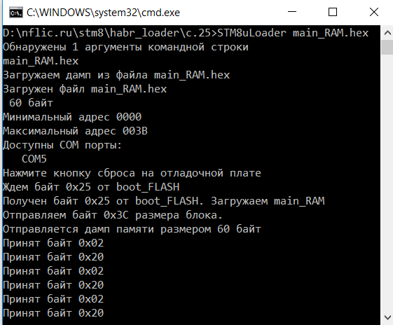
Run the file runSTM8uLoader.bat , press the reset button on the board, the loader sends byte 0x25. A memory dump with the code from the main_RAM.hex file is sent to the STM8 RAM memory. The board starts blinking the LED and sending bytes 0x20 and 0x02. Press the reset button again. The application program starts from FLASH memory, the LED starts blinking faster and sending bytes 0x80 and 0x08.
At the last stage, to write the image of the loader in the OPTION Bytes area, you need to use the method . The essence of the method is that you first need to write the firmware file boot_OPTION_rev25.hex to the FLAH memory STM8 in the FLAH , reload the microcontroller, fill the OPTION Bytes area with the necessary information and the LED will turn on. Then again, the programmer to write in FLASH firmware file from this article boot_FLASH_OPTION.hex .
Added “clean” bootloader version 0x14 code without application code. Deployed the boot_OPTION image to the source code. Corrected comments. Unlike the version $ 25, the address for transferring control to an application program is in $ 9FFE cells: $ 9FFFF of the FLASH memory. The size in FLASH memory is respectively 20 bytes.
Added “clean” loader code version 0x25 without application code. Deployed the boot_OPTION image to the source code. Corrected comments. In contrast to version $ 14, the address of control transfer to an application program is in cells $ 4831: $ 4832 of the OPTION Bytes area. The occupied size in the FLASH memory accordingly decreased to 18 bytes. The occupied size in the OPTION Bytes area has not changed (52 bytes + 1 backup).
Address transfer control application program in FLASH memory, you can choose from a range of $ 8004 ... $ 9FF1. For an application code image from EEPROM memory, transfer of control is possible only at $ 0000 in the RAM memory.
Host program the second command line argument can pass any address transfer control.
The source code of the host program can be found here . There are also contacts for more extensive communication.
I ask readers of targeted criticism and suggestions to further reduce the code.
I propose to read also the article “How to compress the bootloader for STM8 to the size of 8 bytes in FLASH memory” .
The loader was necessary for some device to which it is impossible to connect the programmer.
It was decided to try to write the bootloader on its own with the following requirements:
- the bootloader should be called STM8uLoader;
- the code should be written in assembler (since assembler is not legally prohibited by law);
- the loader should occupy the minimum possible amount in FLASH memory, the volume occupied in the computer will be considered unlimited;
- the loader should not move the table of interrupt vectors;
- the bootloader must have the minimum functionality, the entire main functionality must be assumed by the computer;
- the loader must transfer control to the application program within a reasonable time after resetting / turning on when there is no connection with the computer.
The first condition was instantly fulfilled , but over subsequent requirements had to work.
First stage. 65 byte code in FLASH memory
To save the vector table in its place, it was decided to place the code at the end of the FLASH memory and switch to it immediately from the reset vector $ 8000.
When loading, control is transferred to the loader code at $ 9FC2. The loader configures the UART 9600 8N1, waits for two bytes on the UART, and without waiting for it passes control to the application program at the address stored in the $ 9FFE pair: $ 9FFF.
If the bootloader accepts the high and low bytes of the size of the expected dump from the host program, then takes the dump itself, puts the dump in the RAM memory and transfers control to it.
Further, all care falls on the program in the computer and the dump sent by it. It should send exactly those dumps that are needed to perform the current task (reading / erasing / writing / copying STM8 memory cells). Dumps should be able to replace each other in RAM memory and transfer control to the application program.
The address of the transition to the application program here is $ 9FFE: $ 9FFF.
File boot_FLASH.asm:
stm8/ TITLE  "boot_FLASH.asm"
    .NOLIST
    #include "STM8S103F3P.inc"
	.LIST
    MOTOROLA
    WORDS
    segment byte at 8000 'boot_start'
boot_start:
  jp    boot_FLASH_start
  dc.b  $00 ;версия boot_FLASH
; ********************************************************
; адреса 0x8004...0x9FC1 свободны для прошивки прикладной программы
    WORDS      ;
    segment byte at 8004 'main_FLASH'
main_FLASH_start:
    ldw   X, #$03FF
	ldw   SP, X
    mov    UART1_BRR1, #13
    mov    UART1_CR2, #%00001100
main_FLASH_cycle:
    callr  main_delay
; выключаем светодиод
	bset 	PB_DDR,#5
	bset 	PB_CR1,#5
; отправляем байт
byte1_tx:
   mov    UART1_DR, #$80
byte1_wait_tx
  btjf  UART1_SR, #7, byte1_wait_tx
    callr  main_delay
boot_RAM_exit1:
; выключаем светодиод
	bres 	PB_DDR,#5 		;
	bres 	PB_CR1,#5 		;
; отправляем байт
byte2_tx:
   mov    UART1_DR, #$08
byte2_wait_tx
  btjf  UART1_SR, #7, byte2_wait_tx
	jra main_FLASH_cycle
main_delay:
   decw     X
   jrne    main_delay
   ret
    segment byte at 9FC2 'boot_FLASH'
boot_FLASH_start:
   mov    UART1_BRR1, #13; Fmaster=16/8=2МГц/9600/16
   mov    UART1_CR2, #%00001100;  разрешаем передачу/прием
; отправляем по UART1 содержимое региста RST_SR
boot_FLASH_RST_SR_tx:
   mov    UART1_DR, RST_SR
; это сигнал хост программе, что можно отправлять дамп памяти
; ждем первый байт блока данных
; и перебираем регистр X для отсчета таймаута (примерно 200 миллисекунд)
  ldw    X,#0
boot_FLASH_wait_byte1:
  decw  X
  jreq  boot_FLASH_exit;  по истечению таймаута выходим из бутлоадера
  btjf  UART1_SR, #5, boot_FLASH_wait_byte1
; первый байт принят, прекращаем отсчитывать таймаут,
; регистр X используем для косвенной адресации
  ld    A, UART1_DR
  ld    XH, A
; ждем второй байт блока данных
boot_FLASH_wait_byte2:
  btjf  UART1_SR, #5, boot_FLASH_wait_byte2
; второй байт принят
  ld    A, UART1_DR
  ld    XL, A ; указатель X -количество байт в блоке
; в регистре X количество оставшихся байт в блоке данных
  ldw    Y, #$0400 ; указатель Y на адрес 0x0400 (RAM_END + 1)
; ждем очередной байт
boot_FLASH_rx_block_wait:
  btjf  UART1_SR, #5, boot_FLASH_rx_block_wait
boot_EEPROM_rx_block_entry:
  decw  Y  ; после каждой итерации в регистре Y адрес последнего загруженного байта
  ld    A, UART1_DR
  ld    (Y), A
  decw  X ; после каждой итерации в регистре X количество оставшихся для загрузки байтов
  jrne  boot_FLASH_rx_block_wait
; передаем управление принятому блоку данных
  jp    (Y)
; передаем управление основной (прикладной) программе
boot_FLASH_exit:
  dc.b  $CC
boot_FLASH_exit_addr:
  dc.w  main_FLASH_start
  end
;
Second phase. 21 byte code in FLASH and 52 bytes in EEPROM memory
Selecting 65 bytes from the FLASH memory (in STM8S103F3, its total is 8192 bytes) is not human. After all, the unused EEPROM memory with its 640 bytes is lying around. Let's divide the bootloader code into two parts, boot_FLASH and boot_EEPROM.
When loading, control of the boot_FLASH code is transferred to the address $ 9FEF. boot_FLASH copies the boot_EEPROM code image from EEPROM memory into RAM memory and transfers control to it.
Now the boot_EEPROM configures the UART 9600 8N1, waits for UART bytes, and without waiting for it transfers control to the application program (the address is $ 9FFE: $ 9FFF).
If the boot_EEPROM accepts a byte with the size of the expected dump for RAM memory, then takes a dump, dumps it to another area of RAM memory and transfers control to it.
Then everything is like in the first stage.
File boot_FLASH_EEPROM.asm:
stm8/ TITLE  "boot_FLASH_EEPROM.asm"
    .NOLIST
    #include "STM8S103F3P.inc"
	.LIST
    MOTOROLA
    WORDS
    segment byte at 4000'eeprom'
; образ boot_EEPROM
    dc.b   $35, $0D, $52, $32, $35, $0C, $52, $35
    dc.b   $35, $01, $52, $31, $5A, $27, $16, $72
    dc.b   $0B, $52, $30, $F8, $C6, $52, $31, $72
    dc.b   $0B, $52, $30, $FB, $3B, $52, $31, $4A
    dc.b   $26, $F5, $96, $5C, $FC, $CE, $9F, $FE
    dc.b   $2B, $FA, $90, $AE, $42, $7F, $AE, $02
    dc.b   $7F, $CC, $9F, $F4
    segment byte at 8000'boot_start'boot_start:
  jp    boot_FLASH_start
  dc.b  $01 ;версия boot_FLASH_EEPROM
; ********************************************************
; адреса 0x8004...0x9FEE свободны для прошивки прикладной программы
    segment byte at 8004'main_FLASH'
; прикладная программа
main_FLASH_start:
    ldw   X, #$03FF
	ldw   SP, X
    mov    UART1_BRR1, #13
    mov    UART1_CR2, #%00001100 main_FLASH_cycle:
    callr  main_delay
; выключаем светодиод
	bset 	PB_DDR,#5
	bset 	PB_CR1,#5
; отправляем байт
byte1_tx:
   mov    UART1_DR, #$80
byte1_wait_tx
  btjf  UART1_SR, #7, byte1_wait_tx
    callr  main_delay
boot_RAM_exit1:
; выключаем светодиод
	bres 	PB_DDR,#5 		;
	bres 	PB_CR1,#5 		;
; отправляем байт
byte2_tx:
   mov    UART1_DR, #$08
byte2_wait_tx
  btjf  UART1_SR, #7, byte2_wait_tx
	jra main_FLASH_cycle
main_delay:
   decw     X
   jrne    main_delay
   ret
; начальный копировщик EEPROM -> RAM
    segment byte at 9FEF 'boot_FLASH'boot_FLASH_start:
    ldw     X, SP
; Y <- { EEPROM_START + RAM_END}
; Y <- { $4000 + $03FF = $43FF }
    ldw    Y, #$43FFboot_FLASH_copy:
    ld      A, (Y)
    ld      (X), A
    decw    Y
    decw    X
    jrpl    boot_FLASH_copy
    incw    X
    jp     (X)
boot_FLASH_exit_address:
    dc.w  main_FLASH_start
  end
;
Run the file runSTM8uLoader.bat , press the reset button on the board, the loader sends byte 0x01. A memory dump with the code from the main_RAM.hex file is sent to the STM8 RAM memory. The board starts blinking the LED and sending bytes 0x20 and 0x02. Press the reset button again. The application program starts from FLASH memory, the LED starts blinking faster and sending bytes 0x80 and 0x08.
The third stage. Code size of 18 bytes in FLASH memory and 52 bytes in OPTION Bytes
With the EEPROM memory, of course, we hurried. Where now to store the sinuses and other tables? Yes, and with FLASH memory is not all clear. Who decided to store the transfer address of the control application program in memory FLASH? And the same byte of the bootloader version is generally stored in two places at once. Where to squeeze in 52 bytes intended for EEPROM?
Here we can help lithography. EEPROM memory consists of 10 blocks of 64 bytes each. To add one more block to these blocks, but with a different size is not economically feasible. STMicroelectronics did just that, added another block of 64 bytes in size, called this area OPTION Bytes and stores there the important non-volatile settings of the microcontroller (in STM8S103F3 it is as much as 11 bytes). And of course, STM has forgotten to mention that there are still 53 workable cells in this area. Apparently there are a lot of STM8 models, you need to leave room for future important settings.
Our loader claims only for STM8 models without built-in loaders. For this, we are taking backup cells of the OPTION Bytes block while nobody sees it. The truth is there is one small, but solvableinconvenience. Normal programmer will not allow you to write information in these cells.
When loading, control of the initial copier boot_FLASH is transferred to the address $ 9FF2. boot_FLASH transfers the boot_OPTION bootloader image from the OPTION Bytes area to the RAM memory.
boot_OPTION configures the UART 9600 8N1, sends the UART bytes with its version, waits for the UART bytes from the host program, and without waiting for 0.2 seconds, transfers control to the application program at the address located in the pair $ 4831: $ 4832.
If, after sending a byte with its version, the boot_OPTION accepts a byte of the size of the expected dump, then the dump follows, dumps it into RAM memory and transfers control to it.
Further, all care falls on the program in the computer and the dump sent by it. It should send exactly those dumps that are needed to perform the current task (reading / erasing / writing / copying STM8 memory cells). Dumps should be able to replace each other in RAM memory and transfer control to the application program.
The address of the transition to the application program here is $ 4831: $ 4832.
Code loader and application program to run in flash memory:
stm8/ TITLE  "boot_FLASH_OPTION.asm"
    .NOLIST
    #include "STM8S103F3P.inc"
    .LIST
    MOTOROLA
    WORDS
    segment byte at 4800'boot_OPTION'
; образ начального загрузчика boot_OPTION
    dc.b    $00, $00, $FF, $00, $FF, $00, $FF, $00
    dc.b    $FF, $00, $FF, $35, $0D, $52, $32, $35
    dc.b    $0C, $52, $35, $35, $25, $52, $31, $5A
    dc.b    $27, $16, $72, $0B, $52, $30, $F8, $C6
    dc.b    $52, $31, $72, $0B, $52, $30, $FB, $3B
    dc.b    $52, $31, $4A, $26, $F5, $96, $5C, $FC
    dc.b    $AE, $80, $04, $2B, $FA, $90, $AE, $42
    dc.b    $7F, $AE, $02, $7F, $CC, $9F, $F6, $00
    segment byte at 8000'boot_start'boot_start:
    ldw     X, SP
    jp    boot_FLASH_start
; ********************************************************
; адреса 0x8004...0x9FF1 свободны для прошивки прикладной программы
    segment byte at 8004'main_FLASH'
; прикладная программа
main_FLASH_start:
    ldw   X, #$03FF
	ldw   SP, X
    mov    UART1_BRR1, #13
    mov    UART1_CR2, #%00001100 main_FLASH_cycle:
    callr  main_delay
; выключаем светодиод
	bset 	PB_DDR,#5
	bset 	PB_CR1,#5
; отправляем байт
byte1_tx:
   mov    UART1_DR, #$80
byte1_wait_tx
  btjf  UART1_SR, #7, byte1_wait_tx
    callr  main_delay
boot_RAM_exit1:
; выключаем светодиод
	bres 	PB_DDR,#5 		;
	bres 	PB_CR1,#5 		;
; отправляем байт
byte2_tx:
   mov    UART1_DR, #$08
byte2_wait_tx
  btjf  UART1_SR, #7, byte2_wait_tx
	jra main_FLASH_cycle
main_delay:
   decw     X
   jrne    main_delay
   ret
; начальный копировщик OPTION -> RAM
    segment byte at 9FF2 'boot_FLASH'boot_FLASH_start:
; Y <- { OPTION_START + RAM_END}
; Y <- { $4800 + $03FF = $43FF }
    ldw    Y, #$43FFboot_FLASH_copy:
    ld      A, (Y)
    ld      (X), A
    decw    Y
    decw    X
    jrpl    boot_FLASH_copy
    incw    X
    jp     (X)
boot_FLASH_exit_address:
    dc.w  main_FLASH_start
  end
;
The code of the application program for execution in RAM:
stm8/
	TITLE “boot_RAM.asm”
	MOTOROLA
	#include "STM8S103F3P.inc"
	BYTES
	segment byte at 0000 'boot_RAM_data'
boot_RAM_start:
; Включаем pull-up на портах (если подтяжка не предусмотрена внешней схемой) илине включаем, все равно работает, экономим 14 байт
;  ld    A, #%01001100              ; [A6 4C]
;  cpl    A                         ; [43]
;  ld    PA_CR1, A                  ; [C7 5003]
;  ld    PB_CR1, A                  ; [C7 5008]
;  ld    PC_CR1, A                  ; [C7 500D]
;  ld    PD_CR1, A                  ; [C7 5012] подтяжка на PD6(UART1_RX), PD2, PD1
; настраиваем UART1 на прием/передачу на скорости 9600, остальные настройки по умолчанию (8 бит, нет бита четности, 1 стоповый бит)
;  mov    UART1_BRR2, #0            ; [35 00 52 33]  для Fmaster=16/8=2МГц и 9600
   mov    UART1_BRR1, #13           ; [35 0D 52 32]  для Fmaster=16/8=2МГц и 9600
   mov    UART1_CR2, #%00001100     ; [35 0C 52 35]    UART1_CR2.TEN <- 1  UART1_CR2.REN <- 1  разрешаем передачу/прием
; отправляем байт по UART1
boot_RAM_byte1_tx:
   mov    UART1_DR, #$02
boot_RAM_byte1_wait_tx
  btjf  UART1_SR, #7, boot_RAM_byte1_wait_tx
   ldw    X,#0                      ; [AE 00 00]  boot_FLASH обнуляет содержимое индексного регистра X
boot_RAM_wait1:
   decw    X                          ; [5A]
   jreq    boot_RAM_exit1           ;
   jra     boot_RAM_wait1
boot_RAM_exit1:
; выключаем светодиод
	bres 	PB_DDR,#5 		;
	bres 	PB_CR1,#5 		;
; отправляем байт по UART1
boot_RAM_byte2_tx:
   mov    UART1_DR, #$20          ; [35 11 52 31]
boot_RAM_byte2_wait_tx
  btjf  UART1_SR, #7, boot_RAM_byte2_wait_tx
   ldw    X,#0                      ; [AE 00 00]  boot_FLASH обнуляет содержимое индексного регистра X
boot_RAM_wait2:
   decw    X                          ; [5A]
   jreq    boot_RAM_exit2           ;
   jra     boot_RAM_wait2
boot_RAM_exit2:
; выключаем светодиод
	bset 	PB_DDR,#5 		;
	bset 	PB_CR1,#5 		;
   jra     boot_RAM_byte1_tx
end
Run the file runSTM8uLoader.bat , press the reset button on the board, the loader sends byte 0x25. A memory dump with the code from the main_RAM.hex file is sent to the STM8 RAM memory. The board starts blinking the LED and sending bytes 0x20 and 0x02. Press the reset button again. The application program starts from FLASH memory, the LED starts blinking faster and sending bytes 0x80 and 0x08.
At the last stage, to write the image of the loader in the OPTION Bytes area, you need to use the method . The essence of the method is that you first need to write the firmware file boot_OPTION_rev25.hex to the FLAH memory STM8 in the FLAH , reload the microcontroller, fill the OPTION Bytes area with the necessary information and the LED will turn on. Then again, the programmer to write in FLASH firmware file from this article boot_FLASH_OPTION.hex .
Added “clean” bootloader version 0x14 code without application code. Deployed the boot_OPTION image to the source code. Corrected comments. Unlike the version $ 25, the address for transferring control to an application program is in $ 9FFE cells: $ 9FFFF of the FLASH memory. The size in FLASH memory is respectively 20 bytes.
boot_uC_rev14.asm:
stm8/  TITLE  "boot_uC_rev14.asm" ; boot_uC = boot_OPTION + boot_FLASH
    MOTOROLA
    .NOLIST
    #include "STM8S103F3P.inc"
    .LIST
    WORDS
; ********************************************************
    segment byte at 4800'boot_O_IMG'
;0000FF00FF00FF00FF00FF350D523235
;0C5235351452315A2716720B5230F8C6
;5231720B5230FB3B52314A26F5965CFC
;CE9FFE2BFA90AE427FAE027FCC9FF400
; содержимое конфигурационных регистров
; $4800 не копируется в RAM
    dc.b    $00, $00, $FF, $00, $FF, $00, $FF, $00, $FF, $00, $FF
; OPTION (RAM)
; $480B ($0000)	образ начального загрузчика boot_O
boot_O_start:
; настраиваем UART 96008N1 Fmaster=16/8=2МГц/9600/16
;    mov    UART1_BRR2, #0  ; [35 00 52 33]  исключаем для экономии места
    mov    UART1_BRR1, #13  ; [35 0D 52 32]
; UART1_CR2.TEN <- 1  UART1_CR2.REN <- 1  разрешаем передачу/прием
    mov    UART1_CR2, #%00001100     ; [35 0C 52 35]
; $4813 ($0008)
boot_E_byte1_tx:
; отправляем версию $14 загрузчика
    mov    UART1_DR, #$14 ; [35 14 52 31]
; это сигнал хост программе, что можно отправлять данные
; ждем байт с размером дампа
; регистр X отсчитывает таймаут (примерно 200 миллисекунд)
;    clrw    X          ; [5F] регистр X уже обнулил boot_F
; $4817 ($000C)
boot_O_rx_wait_byte:
    decw  X             ; [5A]
    jreq  boot_O_exit   ; [2716] по истечению таймаута выходим из бутлоадера
    btjf  UART1_SR, #5, boot_O_rx_wait_byte  ; [72 OB 52 30 F8]
; первый байт принят, прекращаем отсчитывать таймаут, регистр A используем как счетчик
; $481F ($0014)
    ld    A, UART1_DR                  ; [C6 5231]
; $4822 ($0017)	ждем очередной байт
boot_O_rx_wait_block:
    btjf  UART1_SR, #5, boot_O_rx_wait_block  ; [72 OB 52 30 FB]push  UART1_DR      ; [3B 5231]
    dec  A              ; [4A]
; после каждой итерации в регистре A количество оставшихся для загрузки байтов
  jrne  boot_O_rx_wait_block       ; [26 F5]
; $482D ($0022)	передаем управление принятому блоку данных
    ldw    X, SP        ; [96]
    incw    X           ; [5C]
boot_O_exit_to_FLASH:
    jp     (X)          ; [FC]
; $4830 ($0025)	передаем управление прикладной программе
boot_O_exit:
    ldw     X, boot_F_exit_address ; [CE 9F FE]
    jrmi    boot_O_exit_to_FLASH   ; [2B FA]
; if X < $8000 адрес пердачи управления равен $0000
; а код находится в EEPROM
boot_O_exit_to_EEPROM:
; Y <- { EEPROM_END}
    ldw     Y, #$427F   ; [90 AE 42 7F]
; X <- { EEPROM_END - EEPROM_START }
; грузим копию EEPROM в RAM
    ldw     X, #$027F   ; [AE 02 7F]
    jp      boot_F_copy ; [CC 9F F4]
; $483F	 ($0034)
    dc.b     $00 ; резервная ячейка
boot_O_end:
; ********************************************************
    segment byte at 8000'RESET_vector'
;96CC9FF0
    ldw   X, SP         ; [96]  X <- RAM_END
    jp    boot_F_start  ; [CC 9F F0]
; ********************************************************
; адреса 0x8004...0x9FEF свободны для прошивки прикладной программы
    segment byte at 8004'main_FLASH'
;20FE
    jra    *            ; [20 FE]
; ********************************************************
; начальный копировщик boot_FLASH
    segment byte at 9FF0'boot_F'
;90AE4C0A90F6F7905A5A2AF85CFC8004
boot_F_start:
; Y <- { boot_O_START + RAM_END} { $480B + $03FF = $4C0A }
    ldw     Y, #$4C0A   ; [90 AE 4C 0A]
; этот участок кода используют
; boot_FLASH, boot_OPTION и дампы из хост программы
boot_F_copy:
    ld      A, (Y)      ; [90 F6]
    ld      (X), A      ; [F7]
    decw    Y           ; [905A]
    decw    X           ; [5A]
    jrpl    boot_F_copy ; [2A F8] если X(Y) >= RAM_START(boot_O_START)
    incw    X           ; [5C]
    jp     (X)          ; [FC]
boot_F_exit_address:
    dc.w  $8004         ; [8004]
;    dc.w  $0000        ; [0000]
  end
;
Added “clean” loader code version 0x25 without application code. Deployed the boot_OPTION image to the source code. Corrected comments. In contrast to version $ 14, the address of control transfer to an application program is in cells $ 4831: $ 4832 of the OPTION Bytes area. The occupied size in the FLASH memory accordingly decreased to 18 bytes. The occupied size in the OPTION Bytes area has not changed (52 bytes + 1 backup).
boot_uC_rev14.asm:
stm8/  TITLE  "boot_uC_rev25.asm" ; boot_uC = boot_OPTION + boot_FLASH
    MOTOROLA
    .NOLIST
    #include "STM8S103F3P.inc"
    .LIST
	BYTES
; ********************************************************
; отсюда стартуют либо образ прикладной прораммы из EEPROM памяти
; boot_O_exit_address должен быть равен $0000 ( проверяется на <$8000)
; либо прикладная программа из файла прошивки
; адрес передается хост программе вторым аргументом в командной строке
    segment byte at 0000'boot_O_IMG'
main_ram:
;20FE
    jra    *            ; [20 FE]
    WORDS
; ********************************************************
    segment byte at 4800'boot_O_IMG'
;0000FF00FF00FF00FF00FF350D523235
;0C5235351452315A2716720B5230F8C6
;5231720B5230FB3B52314A26F5965CFC
;AE80042BFA90AE427FAE027FCC9FF600
; содержимое конфигурационных регистров
; $4800 не копируется в RAM
    dc.b    $00, $00, $FF, $00, $FF, $00, $FF, $00, $FF, $00, $FF
; OPTION (RAM)
; $480B ($0000)	образ начального загрузчика boot_OPTION
boot_O_start:
; настраиваем UART 96008N1 Fmaster=16/8=2МГц/9600/16
;    mov    UART1_BRR2, #0  ; [35 00 52 33]  исключаем для экономии места
    mov    UART1_BRR1, #13  ; [35 0D 52 32]
; UART1_CR2.TEN <- 1  UART1_CR2.REN <- 1  разрешаем передачу/прием
    mov    UART1_CR2, #%00001100     ; [35 0C 52 35]
; $4813 ($0008)
boot_E_byte1_tx:
; отправляем версию $14 загрузчика
    mov    UART1_DR, #$14 ; [35 14 52 31]
; это сигнал хост программе, что можно отправлять данные
; ждем байт с размером дампа
; регистр X отсчитывает таймаут (примерно 200 миллисекунд)
;    clrw    X          ; [5F] регистр X уже обнулил boot_F
; $4817 ($000C)
boot_O_rx_wait_byte:
    decw  X             ; [5A]
    jreq  boot_O_exit   ; [2716] по истечению таймаута выходим из бутлоадера
    btjf  UART1_SR, #5, boot_O_rx_wait_byte  ; [72 OB 52 30 F8]
; первый байт принят, прекращаем отсчитывать таймаут, регистр A используем как счетчик
; $481F ($0014)
    ld    A, UART1_DR                  ; [C6 5231]
; $4822 ($0017)	ждем очередной байт
boot_O_rx_wait_block:
    btjf  UART1_SR, #5, boot_O_rx_wait_block  ; [72 OB 52 30 FB]push  UART1_DR      ; [3B 5231]
    dec  A              ; [4A]
; после каждой итерации в регистре A количество оставшихся для загрузки байтов
  jrne  boot_O_rx_wait_block       ; [26 F5]
; $482D ($0022)	передаем управление принятому блоку данных
    ldw    X, SP        ; [96]
    incw    X           ; [5C]
boot_O_exit_to_FLASH:
    jp     (X)          ; [FC]
; $4830 ($0025)	передаем управление прикладной программе
boot_O_exit:
    dc.b  $AE  ; ldw X, #boot_O_exit_address ; [AE 80 04]
; $4831 ($0026)
; адрес передачи управления прикладной программе
boot_O_exit_address:
    dc.w  main_flash    ; [8004]
;    dc.w  main_ram     ; [0000]
    jrmi    boot_O_exit_to_FLASH   ; [2B FA]
; if X < $8000 адрес пердачи управления равен $0000
; а код находится в EEPROM
boot_O_exit_to_EEPROM:
; Y <- { EEPROM_END}
    ldw     Y, #$427F   ; [90 AE 42 7F]
; X <- { EEPROM_END - EEPROM_START }
; грузим копию EEPROM в RAM
    ldw     X, #$027F   ; [AE 02 7F]
    jp      boot_F_copy ; [CC 9F F4]
; $483F	 ($0034)
    dc.b     $00 ; резервная ячейка
boot_O_end:
; ********************************************************
    segment byte at 8000-8003'RESET_vector'
;96CC9FF2
    ldw   X, SP         ; [96]  X <- RAM_END
    jp    boot_F_start  ; [CC 9F F2]
; ********************************************************
; адреса 0x8004...0x9FF1 свободны для прошивки прикладной программы
    segment byte at 8004'main_FLASH'
main_flash:
;20FE
    jra    *            ; [20 FE]
; ********************************************************
; начальный копировщик boot_FLASH
    segment byte at 9FF2-9FFF 'boot_F'
;90AE4C0A90F6F7905A5A2AF85CFC
boot_F_start:
; Y <- { boot_O_START + RAM_END} { $480B + $03FF = $4C0A }
    ldw     Y, #$4C0A   ; [90 AE 4C 0A]
; этот участок кода используют
; boot_FLASH, boot_OPTION и дампы из хост программы
boot_F_copy:
    ld      A, (Y)      ; [90 F6]
    ld      (X), A      ; [F7]
    decw    Y           ; [905A]
    decw    X           ; [5A]
    jrpl    boot_F_copy ; [2A F8] если X(Y) >= RAM_START(boot_O_START)
    incw    X           ; [5C]
    jp     (X)          ; [FC]
  end
;
Address transfer control application program in FLASH memory, you can choose from a range of $ 8004 ... $ 9FF1. For an application code image from EEPROM memory, transfer of control is possible only at $ 0000 in the RAM memory.
Host program the second command line argument can pass any address transfer control.
The source code of the host program can be found here . There are also contacts for more extensive communication.
I ask readers of targeted criticism and suggestions to further reduce the code.
I propose to read also the article “How to compress the bootloader for STM8 to the size of 8 bytes in FLASH memory” .