Systems in the case or What is actually under the cover of the microprocessor case
The size of transistors in modern microcircuits is inexorably decreasing - despite the fact that Moore’s death has been spoken for several years, and the physical limit of miniaturization is already close (more precisely, in some places it has already been successfully bypassed). However, this decrease does not come in vain, and users' appetites grow faster than the capabilities of chip developers. Therefore, in addition to the miniaturization of transistors, other, often no less advanced technologies are used to create modern microelectronic products.
I deliberately used the phrase “microelectronic product” instead of the word “microcircuit” in the past sentence, because this article will deal with the fact that not a single crystal, but a whole system of several chips can be inside a CPU or GPU case, and called: system in case or system in package.
The term “system in the case” is much less popular than the related term “system on chip”, which developers like to trump. At the same time, almost any chip (except the simplest) is somehow a system on a chip, and the times of microprocessor sets and even individual chips of the south and north bridges are becoming a thing of the past. The advantages of systems on a chip are pretty obvious: fewer cases on the board, less space (and therefore cheaper), less parasitic inductances and capacitances (which means the product will work better and faster), easier for the user (easier to implement and less space for error), cheaper to manufacture (instead of several specialized microcircuits, you can produce one more universal).
But systems on a crystal have their own pitfalls.
First, trying to cram everything into one crystal at once, you risk getting a chip of this size (and with so many legs) that it won't fit into any case. In addition (as the professional technologist suggests in the comments), a very large chip risks not getting into the size of the photolithographic scanner field. It is possible to circumvent this limitation, but it is very difficult technically and, accordingly, very expensive.
Secondly, the larger the chip size, the lower the yield percentage, especially if for the production you need to stitch together several windows on a photo pattern. And this, of course, also affects the cost.
Thirdly, if your system consists of dissimilar components, then combining them all on one chip may be too difficult, too expensive or too bad for the quality of the system. For example, DRAM requires special capacitors, which can be unreasonably expensive to add to a “normal” process for the factory (which, due to this, will be forced to raise prices for customers). Radio frequency or power components on silicon can have significantly worse parameters than on A3B5 materials (gallium arsenide and its analogs), and the combination of digital and analog parts on a single chip creates a noise problem.
The combination of all the above-mentioned factors led to the fact that the trend “we will place everything, everything, everything on one chip” has been replaced by a more balanced approach, as well as to the rapid development of the technology of packing crystals into the case.
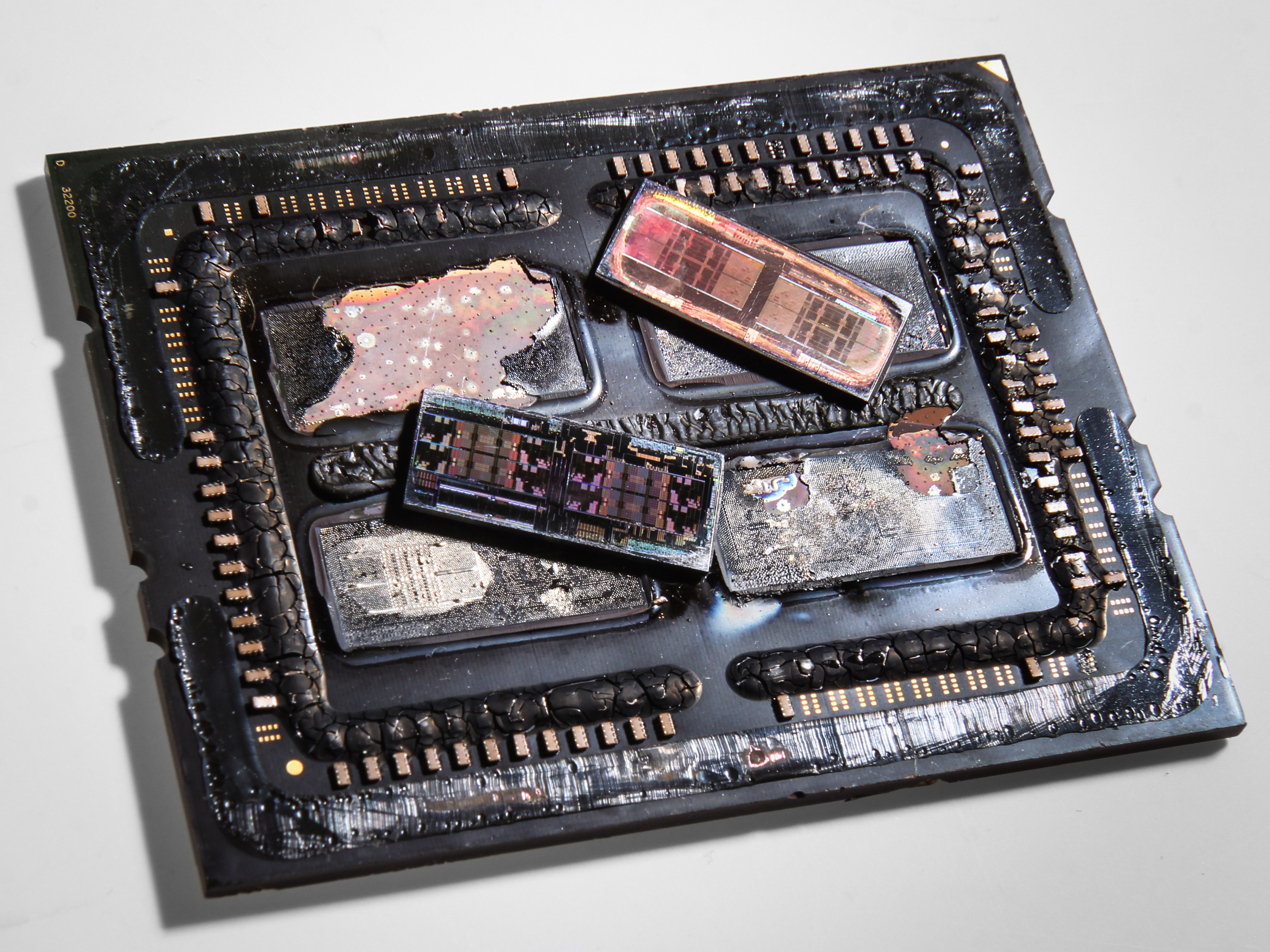
The first example that comes to mind is, of course, AMD microprocessors (see KDPV). Systems in a package for multi-core products are considered to be one of the important reasons for the recent rise of the company, taking place against the background of Intel's problems with the launch of a new technical process due to the low yield on huge chips.
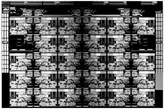
The figure is a 28-core Intel Xeon chip. The size of these processors reaches crazy 456 square millimeters, while the AMD chip size limit is about 200 square millimeters for an eight-core chip, and products with a large number of cores are assembled from several identical crystals on a dual-layer printed circuit board located in the processor case.
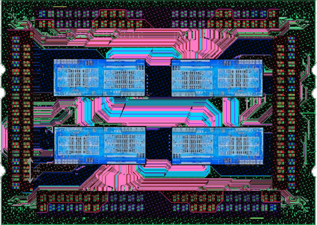
In this figure, you can see the design of the board inside the casing of the EPYC and Threadripper processors (also known as the CDRD). On a two-layer board there are four eight-core crystals. In the case of the Threadripper - c half of the disabled cores. Why are crystals so irrationally used?
First, producing one type of crystal can be cheaper than several different ones.
Secondly, the same applies to the rest of the strapping - disconnecting unnecessary can be cheaper and more technological than developing and producing several different models.
Thirdly, the yield percentage for a 200-millimeter chip, most likely, is also not perfect, and such a design of the final product allows the use of crystals, in which not all cores work. Intel does the same thing, but their problems with getting fit are much stronger due to larger crystals.
And here is another more interesting example, also from AMD. AMD Fiji is a GPU with built-in high-speed memory located right in the case. Why is it important? Because much shorter lines from the processor to the memory allow you to achieve high speeds, and hence greater performance. Unlike the previous example, the crystals inside the case are different. Moreover, there are not five of them, as it may seem at first glance, but much more — twenty-two. Here is the structure section:
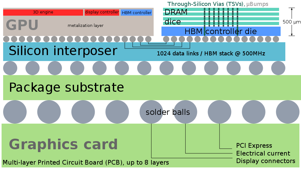
The top layer is the GPU chip itself and a “stack” of several (in this case, four) memory chips connected using TSV (through-silicon-via) - conductive columns that go through the crystal to full thickness.
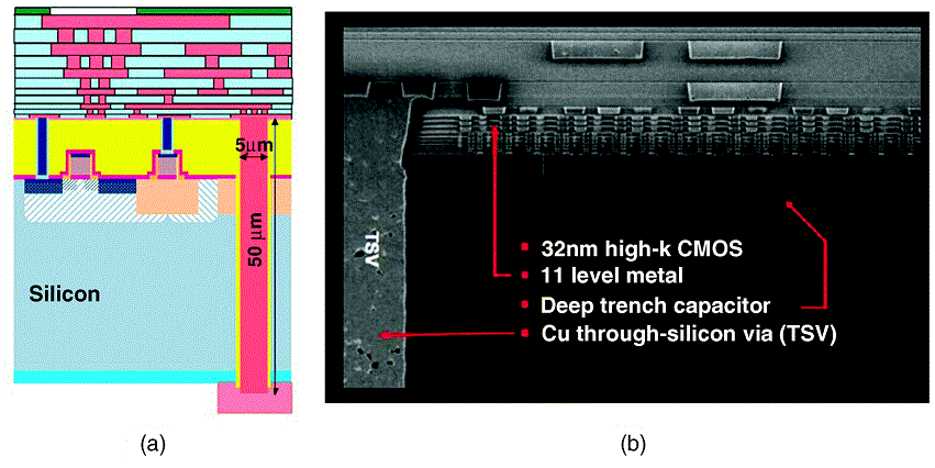
TSV look something like this, schematically and in real scale.
The TSV technology, which originally appeared just for memory arrays (after all, memory does not happen much, right?), Is now becoming more and more widespread, including thanks to the next chip located under the GPU and memory.
Silicon Interposer is a multi-layer PCB substitute made from a silicon chip containing several layers of metallization and TSV for connecting the chips on top and the case. The use of silicon allows to obtain significantly smaller elements (micron units) than a printed circuit board, but the design standards can be rather coarse for this connecting chip to have a high yield and an affordable price. Smaller dimensions of the elements mean less influence on the parasitic parameters of the connections, and the already mentioned TSV is much more compact than vias on the printed circuit board and make it possible to drag hundreds or even thousands of contacts to the case through the interposer. Along with MEMS, such interconnect chips are an important new market for aging factories with plates of 100-150 millimeters in diameter.
Lyrical digression: in the diagram above there is a small but important inaccuracy, contrary to the photograph. Which one?
Another pioneer of 3D integration is Xilinx. Technologically, its FPGAs are close to AMD products (especially those with built-in memory), and the motives are also similar: FPGAs are a market niche where an early transition to a new technical process can give a serious advantage over competitors. According to various estimates, at an early stage in the life of a technology, reducing the size of a crystal by three to four times can raise the yield by two to three times, from a couple of tens of percent to more than half. Moreover, FPGA is a regular structure, on which it is convenient to monitor technological defects. Therefore, FPGA manufacturers are typical “first customers” for new technical processes, and Xilinx, due to the fact that their products contain several small crystals instead of one full-size, can bring new models to the market several months faster than competitors.
Here is a cut of the insides of the Xilinx FPGA. The top chip is the actual part of the FPGA with very small (40-45 µm) contacts to the interposer connecting several chips together, and at the bottom is the base of the case, which has ten layers of its own metal interconnects.
For comparison - Altera FPGA on one huge crystal. Five hundred and sixty square millimeters, Karl! If suddenly this post is read by microelectronic production technologists, take care that they do not have a heart attack.
However, Intel / Altera, of course, does not sit still, watching the success of competitors. Their recent development in the field of systems in the package is the Embedded Multi-Chip Interconnect Bridge (EMIB). It is convenient to look at it on the example of Intel Stratix 10 FPGA.
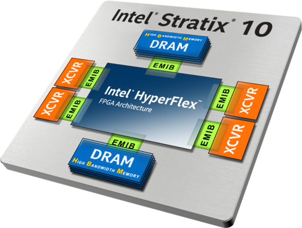
As you can see, EMIB interconnects (one!) The FPGA chip, the memory (and here the multi-storey structures) and peripheral crystals. So what is this EMIB? I wrote a little higher about the silicon interposer, that at the expense of a coarser process it has a much lower price than a chip of the same size, made according to a thin technology. And yet, the interpozer is huge. Is it possible to make it smaller?
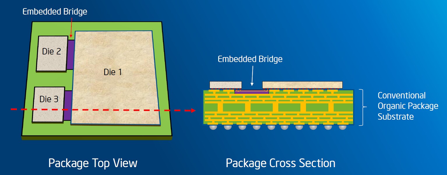
Intel's answer is yes. The idea of EMIB is to use several small interposer instead of one large one, and, in turn, embed them directly into the backing of the case.
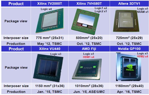
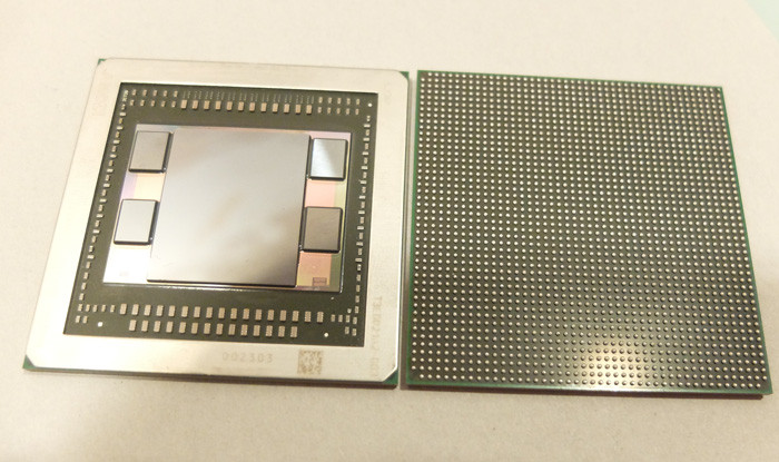
Here is a small selection of products created using silicon interposer. Pay attention to their colossal size by microelectronic standards and to the fact that, as we discussed above, the Xilinx combat chips are divided into several small pieces.
The figure below shows the insides of the Analog Devices ADC case and the circuit diagram. It looks like a completely ordinary printed circuit board for the ADC, only smaller, right? All right, this is it, only due to the use of unpackaged components, the errors associated with parasitic elements have decreased, and the fact that the board was developed in Analog Devices allows them to save a lot of customers' time and at the same time be sure that the user doesn’t have to components or a poorly spreading board.
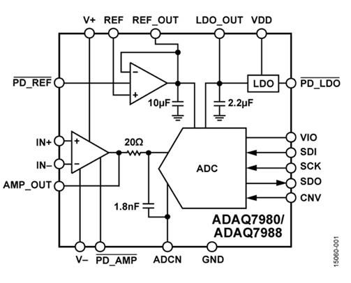
However, there is a little trick in the figure above: can you see crystals laid in two floors? The top crystal is a chip with active components of the ADC itself and (apparently) a dual opamp, and the bottom crystal is passive components (capacitors and resistors). Execution on a separate crystal allows you to make them much larger in size (and therefore reduce errors) without increasing (and therefore more expensive) the main crystal.
All the same can be done on a single chip (which is actually not uncommon, especially for ADCs embedded in microcontrollers), but such a chip will be much more (and therefore, as we found out, there is a risk of a decrease in the yield percentage), and technology for it will have to support all the necessary additional options. In addition, the combination of different blocks on the same crystal will lead to the need to ensure that they do not affect each other (for example, somehow get rid of the noise on the substrate of the crystal).
As we have already found out, the packaging of dissimilar elements (including passive SMD components) in one case allows to significantly reduce the dimensions of the final product and even increase its speed. And what if you use the body itself as a functional element of the device?
In 2013, an integrated voltage regulator (FIVR - fully integrated voltage regulator) was implemented in Intel processors (Haswell microarchitecture), in which the active part of the regulator was implemented on a processor chip, and the passive part (capacitors and inductance) was integrated into the case.
Integral inductance is a headache for all developers of microcircuits, because coils on a crystal are not only obtained with not the best parameters, but also huge (and therefore very expensive, especially on thin technologies). And this is about signal coils without a core, and there is no talk of any transfer of power at all. Intel successfully circumvented this problem by integrating dozens of parallel small coils operating at 160 MHz into the microprocessor case. So they were able to significantly simplify the microprocessor power requirements.
However, with this development, something went wrong, and in the succeeding generations of Intel FIVR processors there was no longer. Since then, it was rumored that they would return to the FIVR, but so far they have remained rumors.
However, even without Intel, the direction of integration of passive components into the case is actively developing, for example, in LTCC (low-temperature ceramics) cases. There, of course, there are limitations and pitfalls (related, for example, with accuracy of nominal values), but this technology is in demand and is actively developing. A multilayer LTCC package looks something like this:
The figure shows all types of passive elements made in multilayer ceramics, and even a metal heat sink (this is a case for a powerful microwave circuit). In fact, it is a mixture of housing with a ceramic printed circuit board. Such pieces are very popular for radio frequency modules, and they are also relatively cheap in small-scale production.
There are a lot of potential applications for the systems in the case, and it is practically impossible to list them all; Moreover, something new is constantly appearing, including due to the fact that these technologies are much more affordable than 10-7-5-3-nanometer transistors.
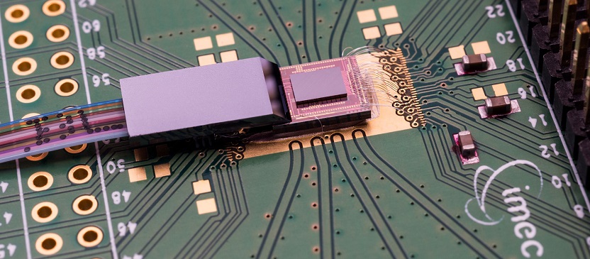
A good example of new applications and properties that opens the integration of heterogeneous chips in a single package is a variety of optical systems, where SiP allows you to put together a receiver or emitter (usually not made on silicon), and their power supply and control circuit. In the illustration below - a prototype of the optical link at 400 Gbit / s (and promise to terabit), assembled at the Belgian research institute IMEC.
In addition, as promising applications for systems in the case, such things as interposers with built-in capillaries for liquid cooling (not only game processors, but also power switches and lasers), MEMS-blocks integrated into the case, and many other interesting things are considered. Moore’s law does not fit within the narrow confines of law. In addition, the ubiquitous Internet of things is considered an important market for systems in the case where small size, the absence of losses (primarily energy, not time) on parasitic elements and the ability to integrate passive components into the case of the chip, for example, parts of the radio path, are important.
I deliberately used the phrase “microelectronic product” instead of the word “microcircuit” in the past sentence, because this article will deal with the fact that not a single crystal, but a whole system of several chips can be inside a CPU or GPU case, and called: system in case or system in package.
The term “system in the case” is much less popular than the related term “system on chip”, which developers like to trump. At the same time, almost any chip (except the simplest) is somehow a system on a chip, and the times of microprocessor sets and even individual chips of the south and north bridges are becoming a thing of the past. The advantages of systems on a chip are pretty obvious: fewer cases on the board, less space (and therefore cheaper), less parasitic inductances and capacitances (which means the product will work better and faster), easier for the user (easier to implement and less space for error), cheaper to manufacture (instead of several specialized microcircuits, you can produce one more universal).
But systems on a crystal have their own pitfalls.
First, trying to cram everything into one crystal at once, you risk getting a chip of this size (and with so many legs) that it won't fit into any case. In addition (as the professional technologist suggests in the comments), a very large chip risks not getting into the size of the photolithographic scanner field. It is possible to circumvent this limitation, but it is very difficult technically and, accordingly, very expensive.
Secondly, the larger the chip size, the lower the yield percentage, especially if for the production you need to stitch together several windows on a photo pattern. And this, of course, also affects the cost.
Thirdly, if your system consists of dissimilar components, then combining them all on one chip may be too difficult, too expensive or too bad for the quality of the system. For example, DRAM requires special capacitors, which can be unreasonably expensive to add to a “normal” process for the factory (which, due to this, will be forced to raise prices for customers). Radio frequency or power components on silicon can have significantly worse parameters than on A3B5 materials (gallium arsenide and its analogs), and the combination of digital and analog parts on a single chip creates a noise problem.
The combination of all the above-mentioned factors led to the fact that the trend “we will place everything, everything, everything on one chip” has been replaced by a more balanced approach, as well as to the rapid development of the technology of packing crystals into the case.
Performance and yield
The first example that comes to mind is, of course, AMD microprocessors (see KDPV). Systems in a package for multi-core products are considered to be one of the important reasons for the recent rise of the company, taking place against the background of Intel's problems with the launch of a new technical process due to the low yield on huge chips.
The figure is a 28-core Intel Xeon chip. The size of these processors reaches crazy 456 square millimeters, while the AMD chip size limit is about 200 square millimeters for an eight-core chip, and products with a large number of cores are assembled from several identical crystals on a dual-layer printed circuit board located in the processor case.
In this figure, you can see the design of the board inside the casing of the EPYC and Threadripper processors (also known as the CDRD). On a two-layer board there are four eight-core crystals. In the case of the Threadripper - c half of the disabled cores. Why are crystals so irrationally used?
First, producing one type of crystal can be cheaper than several different ones.
Secondly, the same applies to the rest of the strapping - disconnecting unnecessary can be cheaper and more technological than developing and producing several different models.
Thirdly, the yield percentage for a 200-millimeter chip, most likely, is also not perfect, and such a design of the final product allows the use of crystals, in which not all cores work. Intel does the same thing, but their problems with getting fit are much stronger due to larger crystals.
And here is another more interesting example, also from AMD. AMD Fiji is a GPU with built-in high-speed memory located right in the case. Why is it important? Because much shorter lines from the processor to the memory allow you to achieve high speeds, and hence greater performance. Unlike the previous example, the crystals inside the case are different. Moreover, there are not five of them, as it may seem at first glance, but much more — twenty-two. Here is the structure section:
The top layer is the GPU chip itself and a “stack” of several (in this case, four) memory chips connected using TSV (through-silicon-via) - conductive columns that go through the crystal to full thickness.
TSV look something like this, schematically and in real scale.
The TSV technology, which originally appeared just for memory arrays (after all, memory does not happen much, right?), Is now becoming more and more widespread, including thanks to the next chip located under the GPU and memory.
Silicon Interposer is a multi-layer PCB substitute made from a silicon chip containing several layers of metallization and TSV for connecting the chips on top and the case. The use of silicon allows to obtain significantly smaller elements (micron units) than a printed circuit board, but the design standards can be rather coarse for this connecting chip to have a high yield and an affordable price. Smaller dimensions of the elements mean less influence on the parasitic parameters of the connections, and the already mentioned TSV is much more compact than vias on the printed circuit board and make it possible to drag hundreds or even thousands of contacts to the case through the interposer. Along with MEMS, such interconnect chips are an important new market for aging factories with plates of 100-150 millimeters in diameter.
Lyrical digression: in the diagram above there is a small but important inaccuracy, contrary to the photograph. Which one?
Another pioneer of 3D integration is Xilinx. Technologically, its FPGAs are close to AMD products (especially those with built-in memory), and the motives are also similar: FPGAs are a market niche where an early transition to a new technical process can give a serious advantage over competitors. According to various estimates, at an early stage in the life of a technology, reducing the size of a crystal by three to four times can raise the yield by two to three times, from a couple of tens of percent to more than half. Moreover, FPGA is a regular structure, on which it is convenient to monitor technological defects. Therefore, FPGA manufacturers are typical “first customers” for new technical processes, and Xilinx, due to the fact that their products contain several small crystals instead of one full-size, can bring new models to the market several months faster than competitors.
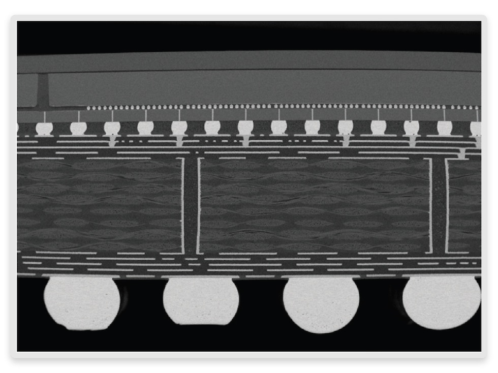
Here is a cut of the insides of the Xilinx FPGA. The top chip is the actual part of the FPGA with very small (40-45 µm) contacts to the interposer connecting several chips together, and at the bottom is the base of the case, which has ten layers of its own metal interconnects.
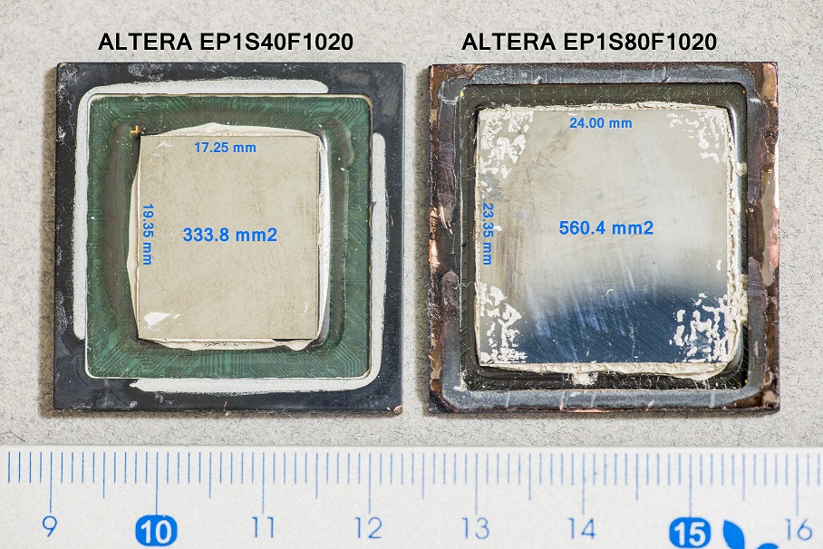
For comparison - Altera FPGA on one huge crystal. Five hundred and sixty square millimeters, Karl! If suddenly this post is read by microelectronic production technologists, take care that they do not have a heart attack.
However, Intel / Altera, of course, does not sit still, watching the success of competitors. Their recent development in the field of systems in the package is the Embedded Multi-Chip Interconnect Bridge (EMIB). It is convenient to look at it on the example of Intel Stratix 10 FPGA.
As you can see, EMIB interconnects (one!) The FPGA chip, the memory (and here the multi-storey structures) and peripheral crystals. So what is this EMIB? I wrote a little higher about the silicon interposer, that at the expense of a coarser process it has a much lower price than a chip of the same size, made according to a thin technology. And yet, the interpozer is huge. Is it possible to make it smaller?
Intel's answer is yes. The idea of EMIB is to use several small interposer instead of one large one, and, in turn, embed them directly into the backing of the case.
Here is a small selection of products created using silicon interposer. Pay attention to their colossal size by microelectronic standards and to the fact that, as we discussed above, the Xilinx combat chips are divided into several small pieces.
More than just performance
The figure below shows the insides of the Analog Devices ADC case and the circuit diagram. It looks like a completely ordinary printed circuit board for the ADC, only smaller, right? All right, this is it, only due to the use of unpackaged components, the errors associated with parasitic elements have decreased, and the fact that the board was developed in Analog Devices allows them to save a lot of customers' time and at the same time be sure that the user doesn’t have to components or a poorly spreading board.
However, there is a little trick in the figure above: can you see crystals laid in two floors? The top crystal is a chip with active components of the ADC itself and (apparently) a dual opamp, and the bottom crystal is passive components (capacitors and resistors). Execution on a separate crystal allows you to make them much larger in size (and therefore reduce errors) without increasing (and therefore more expensive) the main crystal.
All the same can be done on a single chip (which is actually not uncommon, especially for ADCs embedded in microcontrollers), but such a chip will be much more (and therefore, as we found out, there is a risk of a decrease in the yield percentage), and technology for it will have to support all the necessary additional options. In addition, the combination of different blocks on the same crystal will lead to the need to ensure that they do not affect each other (for example, somehow get rid of the noise on the substrate of the crystal).
Additional functions of the case
As we have already found out, the packaging of dissimilar elements (including passive SMD components) in one case allows to significantly reduce the dimensions of the final product and even increase its speed. And what if you use the body itself as a functional element of the device?
In 2013, an integrated voltage regulator (FIVR - fully integrated voltage regulator) was implemented in Intel processors (Haswell microarchitecture), in which the active part of the regulator was implemented on a processor chip, and the passive part (capacitors and inductance) was integrated into the case.
Integral inductance is a headache for all developers of microcircuits, because coils on a crystal are not only obtained with not the best parameters, but also huge (and therefore very expensive, especially on thin technologies). And this is about signal coils without a core, and there is no talk of any transfer of power at all. Intel successfully circumvented this problem by integrating dozens of parallel small coils operating at 160 MHz into the microprocessor case. So they were able to significantly simplify the microprocessor power requirements.
However, with this development, something went wrong, and in the succeeding generations of Intel FIVR processors there was no longer. Since then, it was rumored that they would return to the FIVR, but so far they have remained rumors.
However, even without Intel, the direction of integration of passive components into the case is actively developing, for example, in LTCC (low-temperature ceramics) cases. There, of course, there are limitations and pitfalls (related, for example, with accuracy of nominal values), but this technology is in demand and is actively developing. A multilayer LTCC package looks something like this:
The figure shows all types of passive elements made in multilayer ceramics, and even a metal heat sink (this is a case for a powerful microwave circuit). In fact, it is a mixture of housing with a ceramic printed circuit board. Such pieces are very popular for radio frequency modules, and they are also relatively cheap in small-scale production.
What else?
There are a lot of potential applications for the systems in the case, and it is practically impossible to list them all; Moreover, something new is constantly appearing, including due to the fact that these technologies are much more affordable than 10-7-5-3-nanometer transistors.
A good example of new applications and properties that opens the integration of heterogeneous chips in a single package is a variety of optical systems, where SiP allows you to put together a receiver or emitter (usually not made on silicon), and their power supply and control circuit. In the illustration below - a prototype of the optical link at 400 Gbit / s (and promise to terabit), assembled at the Belgian research institute IMEC.
In addition, as promising applications for systems in the case, such things as interposers with built-in capillaries for liquid cooling (not only game processors, but also power switches and lasers), MEMS-blocks integrated into the case, and many other interesting things are considered. Moore’s law does not fit within the narrow confines of law. In addition, the ubiquitous Internet of things is considered an important market for systems in the case where small size, the absence of losses (primarily energy, not time) on parasitic elements and the ability to integrate passive components into the case of the chip, for example, parts of the radio path, are important.