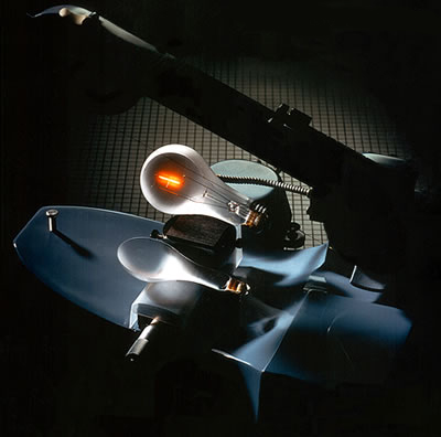
Inside view: LED bulbs
Foreword
Recently, hype has been raised around LED lamps, which should replace ordinary Ilyich lamps. And as the chief nanotechnologist of Russia told , such lamps will soon go on sale in Moscow and St. Petersburg. Of course, everything was furnished with pathos: the first to appreciate the novelty was V.V. Putin. I was able to get the light bulb from Optogan one of the first, besides I got another Russian-made light bulb (Sveta LED or SvetaLED) in my hands, though it’s beaten with life, but it’s working, and Chinese NoName, which can be easily buy on ebay or dealextreme.com.
When I get at least some more or less valuable and interesting item (from eyeshadow to processor or CD, I immediately want to disassemble it and look inside, see how it all works and works. Apparently, this distinguishes scientists from ordinary people. Agree, what a normal person will take apart a light bulb for 1000 rubles, but what to do - the party said: it is necessary!
Theoretical part
Why do you think everyone is so concerned about replacing incandescent bulbs , which have become a symbol of an entire era, with gas discharge and LED ?
Of course, firstly, it is energy efficiency and energy saving. Unfortunately, a tungsten spiral emits more “thermal” photons (ie light with a wavelength of more than 700-800 nm) than gives light in the visible range (300-700 nm). It's hard to argue with that - the chart below will tell you everything for yourself. Given that the power consumption of gas-discharge and LED lamps is several times lower than that of incandescent lamps at the same illumination that is measured in lux. Thus, we get that it is really beneficial for the end user. Another thing is industrial facilities (not to be confused with offices): lighting is an important part, but still the main energy costs are connected precisely with the operation of machine tools and industrial plants. Therefore, all generated gigawatts go to rolling pipes, electric furnaces, etc. That is, real savings in the entire state are not so great.
Secondly, the service life of the lamps that came to replace the "Ilyich bulbs" is several times higher. For an LED lamp, the service life is almost unlimited if the heat sink is properly organized.
Thirdly, it is innovation / modernization / nanotechnology (underline as necessary). Personally, I see nothing innovative in either mercury or LED lamps. Yes, this is a high-tech production, but the idea itself is just a logical application in practice of knowledge about semiconductors, which is 50-60 years old, and materials known for about two decades.
Since the article is devoted to LED lamps, I will dwell on their device in more detail. It has long been known that the conductivity of an illuminated semiconductor is higher than the conductivity of an unlit semiconductor ( Wiki ). In some unknown way, light causes electrons to run through the material with less resistance. Photon, if its energy is greater than the semiconductor band gap (E g), is able to knock an electron out of the so-called valence band and throw it into the conduction band.

The arrangement of zones in a semiconductor. E g - band gap, E F - Fermi energy, numbers indicate the distribution of electrons over states at T> 0 ( source )
We complicate the problem. Take two semiconductors with different types of conductivity n and pand put it together. If in the case of a single semiconductor we simply observed an increase in the current flowing through the semiconductor, now we see that this diode (namely, the pn junction, which occurs at the interface of semiconductors with different types of conductivity) is a mini-source of constant current, and the magnitude of the current will depend on the illumination. If you turn off the light, the effect will disappear. By the way, the principle of operation of solar panels is based on this .

At the junction of p and n type semiconductors, the charges arising after irradiation with light are separated and each "leaves" to its own electrode ( source )
Now back to the LEDs. It turns out that the opposite can also be done: connect the p-type semiconductor to the plus on the battery, and the n-type to the minus, and ... And nothing will happen, there will be no radiation in the visible part of the spectrum, since the most common semiconductor materials (for example , silicon and germanium) are opaque in the visible region of the spectrum. The reason for this is that Si or Ge are not direct-gap semiconductors . But there is a large class of materials that have semiconductor properties and are simultaneously transparent. Bright representatives are GaAs (gallium arsenide), GaN (gallium nitride).
In total, to get an LED, we just need to make a pn junction from a transparent semiconductor. I’ll probably dwell on this, because the further, the more complicated and incomprehensible the behavior of LEDs becomes.
I will allow myself just a few words about modern LED manufacturing technologies. The so-called active layer is a very thin 10-15 nm thick alternating layers of p- and n-type semiconductors, which consist of elements such as In, Ga and Al. Such layers are epitaxially grown using the MOCVD method (metal-oxide chemical vapor deposition or chemical vapor deposition).

Schematic representation of the LED device
There is another problem that prevents the implementation of 100% conversion (conversion of 1 electron to 1 photon) of electricity, and it lies in the fact that even such thin layers of semiconductors to some extent absorb light. It’s not even that they strongly absorb, simply the light “wanders” inside the crystal due to the effect of total internal reflection at the crystal / air interface: the path length until the light exits the crystal increases and, ultimately, such a wandering photon can be absorbed. One solution is to use structured substrates. For example, in the modern LED industry, the molded sapphire substrate method is widely used. Such microstructuring leads to an increase in the efficiency of light output of the entire diode ( more ).
For interested readers, I can offer you to get acquainted with the physics that underlies the work of LEDs. In addition to this interesting work performed within the walls of the native Moscow State University, Svetlana and Optogan have a wonderful galaxy of research teams in St. Petersburg itself. For example, PhysTech . And you can read this article .
Methodical part
All measurements of the lamp spectra were made within 30 minutes (i.e., the background signal changed weakly) in a darkened room using an Ocean Optics QE65000 spectrometer. Here you can read about the device spectrometer. In addition to 10 dependences for each type of lamp, a dark spectrum was measured, which was then subtracted from the spectra of the bulbs. All 10 dependences for each sample were summed and averaged. In addition, each final spectrum was normalized to 100%.

Ocean Optics Spectrometer is a Great Tool in Skillful Hands
The practical part
So let's get started. We have six bulbs in stock: 3 for complete analysis and 3 for comparison (control samples, so to speak):
1. Ilyich’s
lamp 2. Ilyich’s lamp M (that is, a discharge lamp that repeats the usual Ilyich’s bulb in shape)
3. Spiral Ilyich (ordinary gas discharge lamp)
4. LED-lamp from Optogan
5. LED-lamp from Sveta
LED 6. LED-lamp from China NoName

All lamps assembled. We can start!
Spectra
We didn’t see anything supernatural here. Ilyich’s bulb shamelessly lets all the electricity into heat and its color is either yellow or orange. All mercury lamps have a striped spectrum, which in the human eye, as the simultaneous inclusion of 3 pixels (RGB) on the screen (blue lines - ~ 420 nm, green - ~ 550 nm, orange and red - everything above 600 nm), is converted to white.
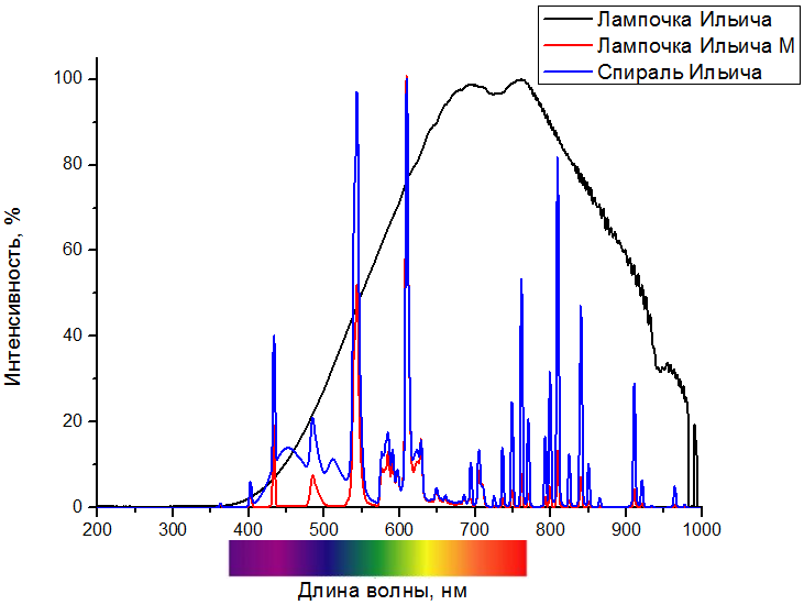
The spectrum of three comparison lamps (for comparison, the part of the spectrum that is perceived by the human eye is presented below the scale)
But the spectrum of LED lamps is strikingly different. There are two components: actually, blue from the diode itself, and the second, smeared throughout the spectrum, from the phosphoror, in Russian, a fluorescent dye, which is applied to the LEDs themselves and poured on top with a protective layer of polymer. The ratio between the blue color of the diode and the emission (emission) band of the phosphor determines the color temperature of the lamp. We can see that Optogan has the warmest light, while China has the coldest. It is advantageous to use 1 phosphor to control the color temperature, thus, the thickness of the phosphor layer in combination with the power of the LED and determines the color temperature. It is worth noting that in bulbs from China and from Svetlana, most likely, the same phosphor is used, but Optogan uses its own (a significant difference between the maximum emission band of the phosphor).
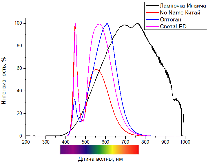
Comparison of the spectra of LED lamps and the traditional Ilyich lamp (for comparison, the part of the spectrum that is perceived by the human eye is presented under the scale)
We got the bulb from Svetlana in a broken form, and we shot the spectrum without frosted glass. However, let me demonstrate a similar situation using the example of a lamp from China, since there were two of them. The normalized spectra differ little among themselves, and a small increase in intensity can be attributed to the fact that longer wavelength radiation is better scattered on frosted glass.

Comparison of Chinese-made lamps with and without a glass bulb (for comparison, the part of the spectrum that is perceived by the human eye is presented below the scale)
If someone is interested, then here rather detailed modeling of LED characteristics is presented.
Price, materials and specifications

They broke three girls under the window late in the evening ... From left to right: Optogan, SvetaLED and NoName China
Chinese NoName
The light bulb from China was ordered through dealextreme.com and delivered to Russia within 2 months (you understand, Russian Post). Its cost is about $ 14 or about 420 rubles, including delivery. The color temperature is 5000-6000K, which corresponds to white cold light. The dimensions are the same as a regular Ilyich bulb. The material of the flask is frosted glass. In my opinion, an ideal replacement for a conventional incandescent lamp if the color temperature were 1000-2000K lower than indicated.
Optogan
The light bulb was presented by mere mortals at a special presentation . Design by Artemy Lebedev, noble materials of the case - polycarbonate and aluminum with the brand name Optogana. The color temperature is 3050 K. A very soft and pleasant lamp, but the price bites - 995 rubles apiece. Who needs it for that kind of money ?!
By the way, Optogan has problems with quality: the endurance test does not pass. Screwed / twisted a couple of times and got the following result:

Flimsy mount. Lady's bulb, what else can I say!
"SvetaLED"
LED llamas of this company have not yet appeared on the Russian market, but they say that the price will be about 450-500 rubles. However, it fell into my hands, packed in a stylish box (apparently, some kind of pilot batch), on which the temperature is 3500-4500K (this is the same as indicating that the length of the equator is from 35,000 km to 45,000 km). The radiator is hidden under an aluminum cap (a trifle, but it’s nice, as if you were holding an ordinary Ilyich’s bulb in your hands, only a little “redone”), and around the aluminum disk with mounted LED modules everything is abundantly covered with KT-8 type thermal grease. They say that Svetlana somehow refers to the military, who apparently live by the principle of Jamie Haineman: "Doubt - Lubricate!". For example, in a Chinese lamp, thermal grease is applied only under the LED modules themselves.
Those who mercilessly beat the Sveta LED and NoName bulbs from China say that the glass is rather fragile, and its quality (a purely subjective assessment) is inferior to incandescent bulbs.
So the bulb was picked ...
On the Optogan lamp chip #RusNT
tag must be put!
And #RusNT will light up for us In
both September and February
(c) AP
A small photo report (for some reason the video camera refused to work) about how we sorted the bulbs:

We need to approach the glamorous experiment glamorously! (Although all color matches are fictitious)

The most important weapon is a hammer, how could one do without it ?!

Honestly, I tried, but polycarbonate never succumbed. Everything was destroyed, a table, linoleum, an aluminum radiator, but not polycarbonate, which was subsequently removed with a screwdriver. But the bulb, even in a half-dismantled state, continued to burn.

Then I had to pick a driver for a very long time, which was flooded with some kind of polymer. As a result, both the driver and Optogan's pride - a monolithic LED chip - were pulled to the surface.
Driver
Below are all 3 drivers together. Rate the complexity of each of them ...
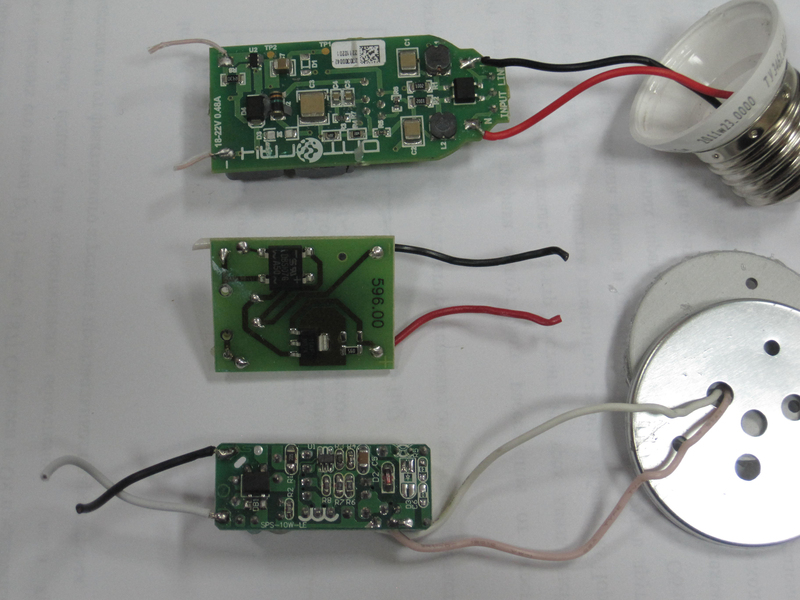
Top to bottom: Optogan, Sveta LED and China
Let's start from the bottom. Honestly speaking, I liked the Chinese driver: powerful capacitors, coils, slightly transforming electronics (diode bridge, etc.). Everything is very compact, which is why the lamp itself is quite modest in size. Also, the big plus is that all lead wires are long, i.e. you can really “repair” the lamp! Or use the driver after the lamp has been used for some other purpose. Of course, most ordinary users do not care about this, but still this can be attributed to potential advantages. The substrate itself with LED chips is mounted on 2 miniature bolts (after all, the Chinese one ...), so, literally, you can treat a lamp like a designer.

The driver from the Chinese NoName LED-lamp The

wiring is really very long ...
The lamp manufactured by Optogan has a very complex driver with solid-state capacitors and, as experts have convinced me, with a switching power supply (although all LED lamps should have such a power supply). At the same time, the driver itself, along with the light-emitting module, is the "chip" of the company and its main pride. Rumor has it that the company will conduct R&D in the field of minimizing this driver and, possibly, in the near future will reduce the size of its giant bulb to an acceptable size.

Pride of Optogan - driver and light-emitting module - next to the main file - base
"SvetaLED". To call it a driver does not turn the language. Even China has some “buns” that improve the consumer properties of the lamp (for example, protect it from blinking), but there is nothing at all, except for a diode bridge, a fuse, a huge capacitor (10 μF, 450 V - a lot or a little ?! it is worth saying that the energy stored in the capacitor is enough for the light bulb to light 1.5 minutes after turning off the power) and, most likely, the load switch. Everything is so simple and primitive that at first I was slightly surprised. The true brainchild of a gloomy Russian genius ...

Also pride ... of a gloomy Russian genius
It is possible that simplicity of execution is the trump card of the Sveta LED light bulb. Flicker with a frequency of 50 Hertz, most likely, the average eye is unlikely to see, and they don’t have anywhere to come from, since a powerful capacitor smoothes everything out and the phosphor cannot even so quickly display the energy pumped into it ( phosphorescence in complex molecular dyes no one canceled). The low cost of the lamp should flow from here ... hmm, but somewhere there is a catch, as the lamp is planned for release at a price close to the Chinese counterpart, taking into account one-time delivery to Russia!
NB It is important to remember that, among other things, the following parameters that are important and dependent on the driver device are: ripple factor, which can adversely affecton the mental activity of a person, and background electromagnetic radiation, which inevitably arises due to the use of various "rectifying" circuits. But this is a completely different story ...
LEDs
So we got to the tidbit of our study. There are many publications on the Internet ( one , two , three ) that compare the spectra of lamps from different manufacturers, their consumer characteristics (design, life, etc.), but now we go down a bit to get closer to the light emitting elements themselves lamps. I must say right away that all 3 lamps are about the same power of 5-6 W (if you carefully look at the technical specifications of the Optogan lamp, we will find an image of this chip designed for 5 W, whereas the declared lamp power is 11 W) and have approximately the same light-emitting area. Total we have a light stream on W ( lumen per W): China - 70-90, Optogan - 65, Svetlana - 75. It seems to me that this is important if dear readers want to compare the lamps among themselves!
To be honest, I was imbued with sympathy for the Chinese LED, namely for the chip itself. The beauty of its internal structure is simply amazing. I was lucky: while I was tearing off all the layers from this LED, I accidentally damaged a large diode chip, as a result of which a microstructured sapphire substrate was exposed:

Optical micrographs of the Chinese chip top view: golden stripes on the chip - current-carrying contacts.

The layered structure of the light emitting chip at maximum magnification with an optical microscope. The dark region corresponds to the sapphire substrate. Arrows indicate individual layers or groups of layers.
By the way, the chip itself is isolated from the outside world by at least 3 layers, but it seems to me that they are still there 4. The first is a polymer with a phosphor, which turns part of the radiation in the blue region of the spectrum into yellow-orange. The second is a small layer of soft polymer, then a convex shell (a la lens) of solid polymer, and two more layers of soft and hard polymers.
I would like to note that, in comparison with other lamps, the Chinese one is as simple as possible. Only 4 wires connect a large chip to the outside world (the rest of the lamps have much more), only 1 light-emitting chip on a diode, which is directly mounted on a board, correctly wired current-carrying contacts on the chip itself, allowing electric current to flow uniformly over the entire surface ( which something like thatthere is also "Optogan"). I could not find any obvious, significant flaws.

SEM images of a structured sapphire substrate. A
layered structure shows that we are on the right track (a consequence of the chip creation method - MOCVD), but it’s unlikely that we can discern individual layers of the active region ... The

chip and contacts that feed it
Let's get down to the Optogan light bulb. The strangest thing, in my opinion, is the location of the light emitting module. In the center. Both China and Svetlana have several “miniature” 1 W modules evenly distributed over the substrate, thus, the heat sink from the LEDs of these companies is much better than from the Optogan module. Yes, I understand very well that the Optogan LED module is made of copper, it conducts heat well, and a large radiator dissipates it efficiently. But the light bulb from Optogan has enormous dimensions, which, by the way, are also due to the fact that it is necessary to somehow fix a polycarbonate flask, and it will fit into not every cartridge.
Such an LED module is arranged quite simply: in a checkerboard pattern, under the polymer layer painted with a yellow-orange phosphor, there are separate diodes that are connected to each other (the connection diagram of the diodes and other technical details can be found here ).

SEM image of individual LEDs on a substrate after removal of the polymer layer
The polymer layer itself has a rather interesting structure. It consists of small (diameter ~ 10 μm) balls:

Optical microphotographs of the “inside” of the polymer layer. It
happened by chance that one diode cut by the microtome remained in the polymer layer. It is worth noting that the diode itself is really transparent and through it the contacts on the other side of the chip are visible:

Optical micrographs of the LEDs on the back: excellent transparency for such products. The
polymer layer is so firmly adhered to both the copper substrate itself and to individual chips that after removing it, a thin polymer layer still remains on the surface of the diodes. Below on the images obtained using an electron microscope, you can see in all its glory the “chip” of the very active layer of the diode, in which the electrons are “converted” into photons:

SEM images of the light-emitting layer of a separate LED (arrows indicate the location of the active layer)

And here is the textured buffer layer, carefully look at the lower right image - it will come in handy for us (the buffer layer is indicated by arrows)

After inaccurate handling of the chip, some contacts were damaged, and some remained intact.
And the last lamp is Sveta LED. The first thing that surprises is the substrate with LED modules - attention! - screwed onto a hefty bolt to the rest of the lamp (just like they did in China). When I took it apart, I thought it might interfere with “tearing” it away from the rest of the lamp, and then I saw a bolt ... By the way, on the back of this aluminum substrate with a marker! some number is written. It seems that at the Svetlana plant near St. Petersburg there are migrant workers who collect these lamps manually. Although no, wait a minute, because the military produces bulbs ... ...

Not only is the substrate with LEDs screwed onto a screw, the number is written on the back ... MARKER - handmade ...
The modules themselves are tightly planted on an aluminum substrate: it is impossible to tear off the whole. Apparently soldered to improve thermal conductivity. I will not comment much here, since all the comments are given above when discussing the Optogan lamp.

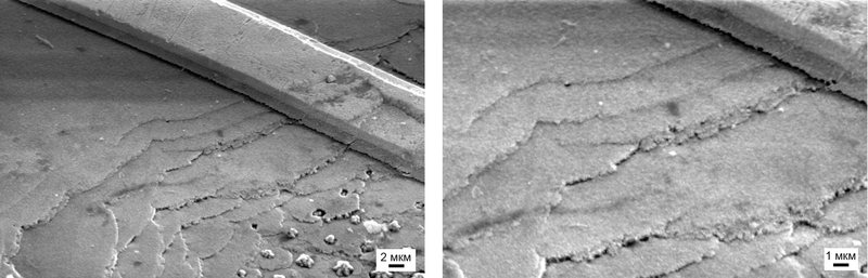
Optical microphotographs of a light-emitting diode from Svetlana's company: the microstructure of the substrate is clearly visible in the insertion image.
Note: I could see how the individual chips are connected in the module from Svetlana. Consistently, to my great disappointment. Thus, if at least 1 LED “burns out”, then the entire module will stop working.

SEM images of a light emitting diode from Svetlana (arrows indicate the active region). In the upper left figure, an image of the proposed contacts is added as they should have been laid in the module (4 x3 diodes).

All the same, the familiar microstructured sapphire substrate ...

Does this picture cause the déjà vu effect ?! The arrows indicate the buffer layer.
Unfortunately, the site of the company manufacturing the Sveta LED lamps was made by true designers: there are a lot of beautiful pictures and little sense, there are no normal meticulous specifications, such as on the Optogana website (by the way, it exists on two RU and COM domains with approximately same content). In addition, there is a site dedicated to only 1 light bulb, there is a site of the company itself , but for some reason the specifications generally lie on a completely different resource .
Scandals, intrigues, investigations…
If someone has read up to this point, now all the fun will begin. Namely, let me just present to your court the data that seemed interesting to me:
1. In this figure I tried to bring photos with some characteristic features of the diodes from Svetlana and Optogan:

2. Carefully read the specification on the website “ Optogana ” and on the site of“ Svetlana ” . The module at Svetlana has dimensions of 5 by 5 mm, 2 corners on the “cover” are cut at 45 degrees, etc. - Much coincides with the specification of Optogan. Does the continuing effect of déjà vu not torment ?! Or maybe everything is purchased in Taiwan ?!
And of course, the conclusions
Are you ready to be a patriot and call the lamp “domestic” (for example, Optogan’s chips are manufactured in Germany) produced the best combination of all factors ?! Perhaps not. Honestly, the Chinese-made LED lamp pleased me pleasantly: the relative simplicity of the diode power circuit, simple materials, and the successful placement of the LEDs on the substrate. The problem with the color temperature is solvable, but the only minus that confuses me as a buyer is the durability of the light bulb from the Middle Kingdom.
Lamps of "domestic" production, and in particular, "Optogan", as always, "please" with their price. I’m more than sure that it would be possible to start with a “handicraft” design, cheap materials (glass instead of polycarbonate) and fill the niche of budgetary light sources (it seems that there are not so many rich people in Russia, or I don’t know something ?! ) But even this is not the main thing, there are quite a few who are ready to invest 1000 rubles in a light bulb and not think about buying them for several years. Let's leave the striking external resemblance between the modules, I am more worried about something else - the resemblance between individual LED chips (geometric dimensions, location, contacts, etc.). It seems that they were manufactured on equipment of the same company, only versions of this equipment differ as v.1.0 and v.1.1. Of course I understand,
Nevertheless, if Optogan company completes the base, removes expensive materials (polycarbonate), reduces its size, replaces 1 powerful chip with a few simpler ones and optimizes the driver (in short, you understand, it will completely remodel the lamp), then such a lamp will have everything chances to conquer the Russian market, since in addition to these shortcomings, there are many advantages such as the competent connection of the diodes in the module, the smart “driver”, etc. Thanks to the technical documentation.
As for Svetlana, in addition to the simplest driver, which should affect the price downward, the location of the light-emitting modules on the substrate, there are practically no pluses. The technical documentation is cloudy, the LEDs are connected in series, which, when a 1 diode “burns out,” destroys the whole module (that is, in our case it reduces the light flux by 12.5%), thermal grease spread everywhere - this does not add confidence. But, it was just a prototype, maybe industrial designs would be better.
This article is not intended to denigrate, or vice versa, the exaltation of the products of some manufacturers over others. I give only the facts, let alone you draw a conclusion! As they say, think for yourself, decide for yourself ...
Video section
Thank you very much OSRAM for preparing such a detailed video on how it produces LEDs (though this company makes LEDs using a slightly different technology than all the bulbs we studied):
The process of carrying LED chips inside a plastic case:
And so, in Taiwan, LED chips are “packed up” using plastic modules with dye application and packaging in bobbins:
Spectral characteristics
The files themselves for analysis can be downloaded here (I hope the people won’t let you down). For spectral characteristics, we thank lezginko and his colleague Anton (if a colleague needs an invite, please write).
In short, then:
The highest quality light from an incandescent lamp (Ra = 96). In second place is a traditional and well-established technology - fluorescent lamps (Ra = 82 and 85). On the third are LED bulbs. Among the LED bulbs, the places were distributed as expected - in the first place were German-Russian Optogan bulbs (Ra = 80), in second and third places were Chinese bulbs (Ra = 70) and Russian Svetlana bulbs (Ra = 68).
PS On Wednesday (26.10) the Nanotechnology Forum will begin, Optogan company will be widely represented at it. I hope that my microphone at the press conference will not be turned off and I will be able to ask uncomfortable questions ... The main thing is to get out alive ... Later comments and my own thoughts were published here .
First , a complete list of published articles on Habré:
Opening the Nvidia 8600M GT chip , a more detailed article is given here: Modern chips - an inside view Inside
view: CD and HDD
Inside view: LED bulbs
Inside view: LED industry in Russia
Inside view: Flash -memory and RAM
Inside view: the world around us
Inside view: LCD and E-Ink displays
Inside view: digital camera arrays
Inside view: Plastic Logic
Inside view: RFID and other marks
Inside view: graduate school in EPFL. Part 1
Inside Look: Graduate School at EPFL. Part 2
Inside view: the world around us - 2
Inside view: the world around us - 3
Inside view: the world around us - 4
Inside view: 13 LED lamps and a bottle of rum. Part 1
Inside view: 13 LED lamps and a bottle of rum. Part 2
Inside view: 13 LED lamps and a bottle of rum. Part 3
Inside Look: IKEA LED Strikes Back
Inside Look: Are Filament Lamps So Good?
and 3DNews:
Microview: comparing displays of modern smartphones
. Secondly , in addition to the HabraHabr blog , articles and videos can be read and viewed on Nanometer.ru , YouTube , and Dirty .
Thirdlyif you, dear reader, liked the article or you want to stimulate writing new ones, then proceed according to the following maxim: "pay what you want"
Yandex.Money 41001234893231
WebMoney (R296920395341 or Z333281944680)
Sometimes it is possible to read briefly, and sometimes not so much about the news of science and technology on my Telegram channel - we are welcome;)