Processor Design (CPU Design) Verilog
- Tutorial
Part I
Part II
Part III
Part IV
Part V We
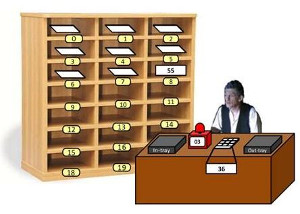
design the Little Man Computer in the Verilog language.
The article about LMC was on Habré.
Online simulator of this computer is here .
We write the RAM / RAM module consisting of four (N = 2) four-bit (M = 4) words. The data is loaded into the RAM of data_in at adr by pressing the button.
module R0 #(parameter N = 2, M = 4)
(
input RAM_button, //кнопка
input [N-1:0] adr, //адрес
input [M-1:0] data_in, //порт ввода данных
output [M-1:0] RAM_out //порт вывода данных
);
reg [M-1:0] mem [2**N-1:0]; //объявляем массив mem
always @(posedge RAM_button) //при нажатии на кнопку
mem [adr] <= data_in; //загружаем данные в ОЗУ из data_in
assign RAM_out = mem[adr]; //назначаем RAM_out портом вывода данных
endmodule
As an external generator, we will connect a 555 CMOS timer (running from 3.3V).
We connect the timer 555 to the counter, we connect the counter to the address input of the RAM .
module R1 #(parameter N = 2, M = 4)
(
input timer555, RAM_button,
//input [N-1:0] adr,
input [M-1:0] data_in,
output [M-1:0] RAM_out
);
reg [1:0]counter; //объявляем счётчик
always @(posedge timer555) //при поступлении тактового сигнала
 counter <= counter + 1;  // счетчик увеличивается на 1
 wire [N-1:0] adr;
 assign adr = counter; // подключаем счётчик на адресный вход ОЗУ
reg [M-1:0] mem [2**N-1:0];
always @(posedge RAM_button)
 mem [adr] <= data_in;
assign RAM_out = mem[adr];
endmodule
Add a load function to the counter.
Loading is done with the Counter_load command .
//input Counter_load;
wire [3:0] branch_adr; // адрес перехода
assign branch_adr = data_in;
always @(posedge timer555)
begin
 if(Counter_load) //по команде "Counter_load"  переходим по адресу  "branch_adr"
  counter <= branch_adr;
 else
  counter <= counter + 1;
end
In a separate module, create a 4bit register (battery).
module register4
(
  input  [3:0] reg_data,
  input reg_button,
  output reg [3:0] q
);
always @(posedge reg_button)
     	 q <= reg_data;
endmodule
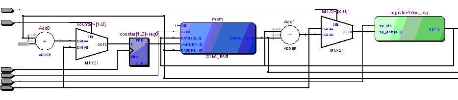
Add to the general scheme Acc battery , MUX2 multiplexer and sum adder .
The adder adds to the number in the battery Acc numbers from the memory.
The data inputs of the multiplexer are served by the data_in and sum numbers .
Then the number from the multiplexer MUX2 is loaded into the battery Acc .
module R2 #(parameter ADDR_WIDTH = 2, DATA_WIDTH = 4)
(
input timer555, Counter_load, RAM_button,
input MUX_switch,
input Acc_button,
input [3:0] data_in,
output [3:0] Acc,
output [DATA_WIDTH-1:0] RAM,
output reg [1:0] counter
);
wire [1:0] branch_adr;
assign branch_adr = data_in[1:0];
//Counter
always @(posedge timer555)
begin
 if(Counter_load)
  counter <= branch_adr;
 else
  counter <= counter + 1;
end
wire [ADDR_WIDTH-1:0] adr;
assign adr = counter;
//RAM
reg [DATA_WIDTH-1:0] mem [2**ADDR_WIDTH-1:0];
always @(posedge RAM_button)
mem [adr] <= Acc;
assign RAM = mem[adr];
//sum
wire [3:0] sum;
assign sum =  Acc + RAM;
//MUX
reg [3:0] MUX2;
always @*
MUX2 = MUX_switch ? sum : data_in;
//Accumulator
register4 Acc_reg(
.reg_data(MUX2),
.reg_clk(Acc_button),
.q(Acc)
);
endmodule
Add an element to the main module that subtracts the numbers in the memory from the number in the battery.
wire [3:0] subtract;
assign subract =  Acc - RAM ;
Replace the two-input multiplexer with a four-input multiplexer.
always @*
MUX4 = MUX_switch[1] ? (MUX_switch[0] ? RAM : subtract)
: (MUX_switch[0] ? sum : data_in);
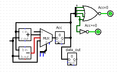
Connect an output device to the battery (4bit register), also connect 2 flags to the battery:
1. The “Zero” flag is a log. element 4ILE or NOT. The flag is raised if the contents of the ass is zero.
2. The “Zero or Positive Number” flag is a log. the item is NOT on the high-order discharge of the four-digit battery. The flag is raised if the contents of the Ass is greater than or equal to zero.
//флаг "Ноль"
output Z_flag;
assign Z_flag =  ~(|Acc); // многовходовой вентиль ИЛИ
//флаг "Ноль или Положительное число"
output PZ_flag;
assign PZ_flag =  ~Acc[3];
Add three commands
1. load the contents of the battery to the data_out output device
2. load the address into the counter if the zero flag is raised ( JMP if Acc = 0)
3. load the address into the counter if the zero or positive number flag is raised ( JMP if Acc > = 0)
module R3 #(parameter ADDR_WIDTH = 2, DATA_WIDTH = 4)
(
input timer555, RAM_button,
input JMP, Z_JMP, PZ_JMP,
input [1:0] MUX_switch,
input Acc_button,
input Output_button,
input [3:0] data_in,
output [3:0] Acc,
output [3:0] data_out,
output [DATA_WIDTH-1:0] RAM,
output Z_flag, PZ_flag,
output reg [1:0] counter
);
wire [1:0] branch_adr;
assign branch_adr = data_in[1:0];
wire Z,PZ;
assign Z = Z_flag & Z_JMP;
assign PZ = PZ_flag & PZ_JMP;
//Counter
always @(posedge timer555)
begin
 if(JMP|Z|PZ)
  counter <= branch_adr;
 else
  counter <= counter + 1;
end
wire [ADDR_WIDTH-1:0] adr;
assign adr = counter;
//RAM
reg [DATA_WIDTH-1:0] mem [2**ADDR_WIDTH-1:0];
always @(posedge RAM_button)
mem [adr] <= Acc;
assign RAM = mem[adr];
//sum
wire [3:0] sum;
assign sum =  Acc + RAM;
//subtract
wire [3:0] subtract;
assign subtract =  Acc - RAM;
//MUX
reg [3:0] MUX4;
always @*
MUX4 = MUX_switch[1] ? (MUX_switch[0] ? RAM : subtract)
: (MUX_switch[0] ? sum : data_in);
register4 Acc_reg(
.reg_data(MUX4),
.reg_clk(Acc_button),
.q(Acc)
);
register4 Output_reg(
.reg_data(Acc),
.reg_clk(Output_button),
.q(data_out)
);
assign Z_flag =  ~(|Acc);
assign PZ_flag =  ~Acc[3];
endmodule
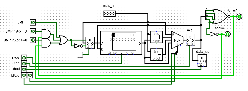
Put the commands and addresses in one RAM / RAM, and the data - in another.
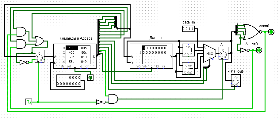
The scheme can be downloaded from here .
Commands are stored in the first eight digits, the address loaded into the counter is stored in the last four digits.
I note that the loading of the number into the accumulator Ass should be done after switching the multiplexer MUX (for commands ADD , SUB , LDA ), according to the decay of the clock signal.
So In our computer, the following command system
48x - ADD add a number from RAM to Ass
50x - SUB subtract the number stored in RAM from Ass
80x - STA save the number from the battery Ass to RAM at x
58x - LDA load the number from address x to Ass
04x - BRA unconditional transition to the cell with the address x
02x - BRZ transition to the cell with the address x if Ass = 0 (conditional transition)
01x - BRP transition to the cell with the address x, if Ass > = 0 (conditional transition)
40x - INP load the number from data_input to Ass
20x - OUT we will not have the number from Ass to data_out. HLT
commands . Take for example the algorithm for finding the maximum of two numbers from http://peterhigginson.co.uk/LMC/ The algorithm works like this: save two numbers from data_in in the data memory. Subtract the first from the second number:
- if the result is negative, write the first number in Ass, write in the data_out the number from Ass;
- if the result is positive, write the second number in Ass, write the number from Ass in the data_out.
00 INP

01 STA 11

02 INP

03 STA 12

04 SUB 11

05 BRP 08

06 LDA 11

07 BRA 09

08 LDA 12

09 OUT
In our command system, this algorithm will look like this. The element is NOT at the control input of the counter, necessary for loading data into the counter - this is a feature of Logisim, in real schemes the element is NOT at the control input not required (at least I don’t know such counters). Quartus II can be downloaded from the official site . When registering in the My Primary Job Function is * section, select Student. Next, you need to download the driver for the programmer (the driver for usb-blaster can be installed from C: \ altera \ ... \ quartus \ drivers \ usb-blaster). Logisim can be downloaded here .
400

80b

400

80c

50b

018

58b

049

58c

200