SamsPcbGuide Part 3: Printed Track Current Limit
Jokes aside, the topic is serious, fire dangerous. Go. This is the third article from the cycle; it considers models for estimating the current limit of a printed circuit, which in some situations is a determining parameter when choosing the thickness of the conductive layers of a printed circuit board.
The previous article said that the choice of the thickness of the copper layers of a printed circuit board is determined primarily by the required minimum gap and minimum width of the conductor, as well as the maximum current flowing through the conductor. These parameters may contradict each other: the thinner the conductive layer, the smaller the topological pattern can be obtained, but the smaller the current limit the printed circuit will withstand (other things being equal, the width of the conductor, the frequency of the current, the heat sink, etc.). Heat energy Q released on the ohmic resistance R of the printed circuit (Joule heat Q = I 2Rt, where I is the current strength, t is time), causes an increase in its temperature relative to the environment, leading to overheating of the conductor itself and its related components or, in extreme cases, to its burnout under the limiting current (eng. Fusing current). The ratio between the current through the printing track and the temperature increase depends on many parameters and is generally difficult to imagine, however, there are formulas for making preliminary estimates.
One of the first attempts belongs to W.G. Pris (WHPreece). He received his empirical dependence in a laboratory experiment in which he gradually increased the current through a conductor until it was red-hot. Pris's formula connects the filament current with a conductor diameter d for various materials:

where K is a table constant approximately equal to 80 for copper. Using the ratio of the area of a circle, you can rewrite this formula for the case of a copper conductor with a cross-sectional area S:

In Pris's experiment, the conductor was suspended in the air, unlike the conductor on a printed circuit board, the conditions of the heat sink for which are completely different. Closer are the conditions of the heat sink for cases of a single connecting conductor, as well as for some cases of microwire splicing (when compounding is not used to protect it), where this formula can give a good estimate for the limiting current.
A permissible increase in the temperature of the printed circuit is usually considered 10-30 ˚C. This value may be more depending on the parameters of the project, but throughout the entire range of product working temperatures the track temperature must be less than the glass transition temperature of the printed circuit board material (English glass transition temperature, T g) and the more heat of copper. Therefore, the dependence of the temperature increase ∆T on the current I of the printed track of width w and foil thickness h, given by D. Brooks in [1], is useful:

where C, α, β, γ are constants, the values of which for the outer and inner layers are given in table 1. It should be borne in mind that on the outer layers the foil thickness is usually 20-40 µm more relative to the base value due to the additional spraying when creating transitional holes. Also, the effect of the finish coating on unmasked boards can be significant. This is used in power devices, when an additional solder is soldered to the printed track opened from the mask.

Another well-known formula for calculating the maximum current-carrying capacity of a conductor is the OnderDonka formula (the IMOnderdonk), which contains such an important parameter as time. It connects the time t of current flow I through a copper conductor with cross section S and the temperature increase ∆T relative to the initial temperature T 0 :

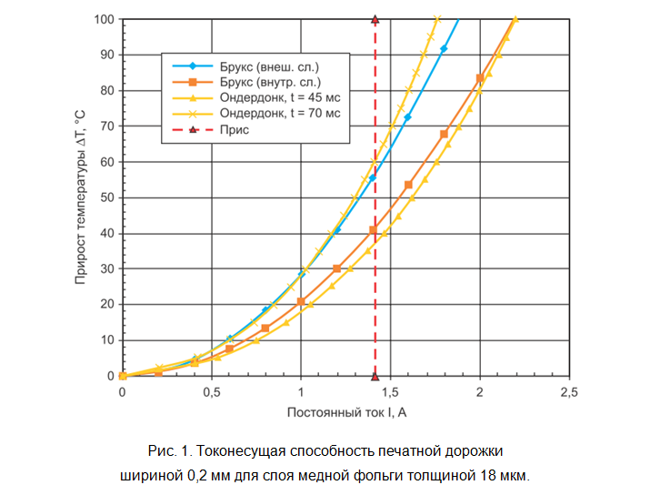
Since the derivation of the formula [2] excludes any heat sink, then for the case of the printed track this formula is applicable for a short current pulse with a duration of up to 1-2 seconds. With increasing time and influence of the heat sink, the accuracy of the estimate decreases, at times understating the limiting current. Graphs of dependencies for all three given formulas for various parameters of the printed track are shown in Figures 1 and 2.

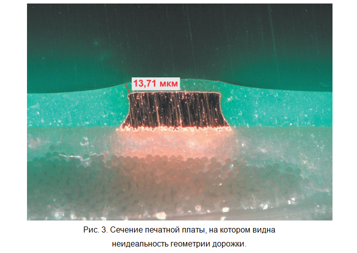
It is always important to consider the experimental conditions or analytical assumptions in the derivation in order to understand the limits of applicability of a particular formula. None of the above formulas will give an accurate and optimal ratio between the limiting current and the required conductor cross section for real applications. The same applies to simple calculators that can be found on the Internet ( for example) because they are based on these or similar formulas. The influence of neighboring conductors and components as sources and receivers of heat, radiation, active or passive cooling can be taken into account only in thermoelectric modeling in specialized CAD systems (such as Cadence, ANSYS, and others). However, even in this case, the results of simulation and experiment may differ significantly. The fact is that the printed track has not a rectangular section, but close to a trapezoid (Fig. 3), and its width and conductivity value of copper foil may not only differ from those calculated by the model, but also have some variation from sample to sample, batches to the party, manufacturer to manufacturer, etc. The influence of the deviations of the width increases with its decrease. However, The calculated results of the formulas and recommendations of the standards will most often represent the worst case, thereby ensuring the safety margin of the system. If the developer needs to optimize the ratio between the limiting current and the required cross-section of the printed track, then it is necessary to go to this goal iteratively through modeling and experiment.
The increase in the cross-section of the printed track proportionally reduces its ohmic resistance per unit length, which reduces thermal losses during the flow of direct current. The situation with alternating current is not so simple due to the existence of a skin effect (eng. Skin effect), which leads to the fact that the alternating current density is unevenly distributed over the cross section of the conductor, exponentially decreasing to zero from the surface of the conductor to the center. For convenience of calculations, the concept of an effective conductor cross section is used with a depth determined by the relation:

where f is the frequency of the current, σ is the conductivity of the metal, μ is the magnetic permeability. At a depth δ equal to the current density becomes smaller in e times the surface current density J S . Mathematically, it is possible to show the correctness of the following approximate equality for the current density J (x, y) in a conductor:

That is, for approximate calculations, it can be assumed that the current flows only in the boundary layer of the perimeter conductor l with a depth of δ, and with a uniform distribution (Fig. 4).

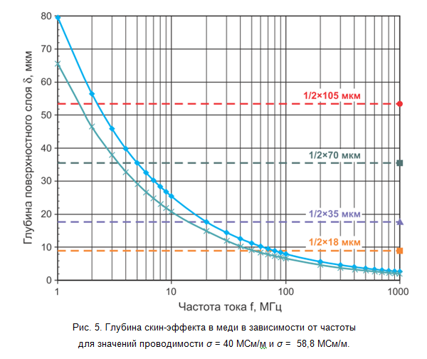
Within this simplified model, if the depth of the surface layer is less than half the thickness of the printed track, then the impedance of the printed track at this frequency will be determined by this effective cross section, leading to an increase in ohmic resistance and a slight decrease in inductance. In fig. 5 shows the dependence of the depth of the surface layer on the frequency of the current, taking into account the variation in the conductivity of the deposited copper. It shows that for copper layers 18 μm thick, the cutoff frequency (above which the skin effect plays a role) is in the region of 50–70 MHz, and for layers of 35 μm in thickness - in the region of 15–20 MHz. Note that at frequencies above 100 MHz, the depth of the skin effect varies only slightly, which allows us to neglect its dependence on frequency when calculating for high-frequency signals.
When designing printed circuit boards with continuously operating currents of several amperes, it is necessary to perform thermal calculations for both electrical components and conductors. The presented models and analytical relations allow us to estimate the current limit of the printed tracks and, on its basis, select the required thickness of the copper layers and the topology of the conductors. To obtain an exact solution, it is necessary to use specialized CAD systems, while it is desirable to specify the geometry, taking into account the technological manufacturing errors and copper conductivity data obtained from the manufacturer of printed circuit boards. I highly recommend to read the articles. D. Brooks, devoted to a detailed analysis of methods for estimating the temperature of the printed conductors, which presents the visual results of modeling temperature fields.
[1] Brooks DG, Adam J. “Trace Currents and Temperatures Revisited”, UltraCAD, 2015.
[2] Adam J., Brooks DG “In Search For Preece and Onderdonk”, UltraCAD, 2015. The
article was first published in the journal Components and technologies ”2018, №1. The publication on “Geektimes” is coordinated with the editors of the magazine.
The previous article said that the choice of the thickness of the copper layers of a printed circuit board is determined primarily by the required minimum gap and minimum width of the conductor, as well as the maximum current flowing through the conductor. These parameters may contradict each other: the thinner the conductive layer, the smaller the topological pattern can be obtained, but the smaller the current limit the printed circuit will withstand (other things being equal, the width of the conductor, the frequency of the current, the heat sink, etc.). Heat energy Q released on the ohmic resistance R of the printed circuit (Joule heat Q = I 2Rt, where I is the current strength, t is time), causes an increase in its temperature relative to the environment, leading to overheating of the conductor itself and its related components or, in extreme cases, to its burnout under the limiting current (eng. Fusing current). The ratio between the current through the printing track and the temperature increase depends on many parameters and is generally difficult to imagine, however, there are formulas for making preliminary estimates.
Pris, Onderdonk and Brooks
One of the first attempts belongs to W.G. Pris (WHPreece). He received his empirical dependence in a laboratory experiment in which he gradually increased the current through a conductor until it was red-hot. Pris's formula connects the filament current with a conductor diameter d for various materials:

where K is a table constant approximately equal to 80 for copper. Using the ratio of the area of a circle, you can rewrite this formula for the case of a copper conductor with a cross-sectional area S:

In Pris's experiment, the conductor was suspended in the air, unlike the conductor on a printed circuit board, the conditions of the heat sink for which are completely different. Closer are the conditions of the heat sink for cases of a single connecting conductor, as well as for some cases of microwire splicing (when compounding is not used to protect it), where this formula can give a good estimate for the limiting current.
A permissible increase in the temperature of the printed circuit is usually considered 10-30 ˚C. This value may be more depending on the parameters of the project, but throughout the entire range of product working temperatures the track temperature must be less than the glass transition temperature of the printed circuit board material (English glass transition temperature, T g) and the more heat of copper. Therefore, the dependence of the temperature increase ∆T on the current I of the printed track of width w and foil thickness h, given by D. Brooks in [1], is useful:

where C, α, β, γ are constants, the values of which for the outer and inner layers are given in table 1. It should be borne in mind that on the outer layers the foil thickness is usually 20-40 µm more relative to the base value due to the additional spraying when creating transitional holes. Also, the effect of the finish coating on unmasked boards can be significant. This is used in power devices, when an additional solder is soldered to the printed track opened from the mask.

Another well-known formula for calculating the maximum current-carrying capacity of a conductor is the OnderDonka formula (the IMOnderdonk), which contains such an important parameter as time. It connects the time t of current flow I through a copper conductor with cross section S and the temperature increase ∆T relative to the initial temperature T 0 :

Since the derivation of the formula [2] excludes any heat sink, then for the case of the printed track this formula is applicable for a short current pulse with a duration of up to 1-2 seconds. With increasing time and influence of the heat sink, the accuracy of the estimate decreases, at times understating the limiting current. Graphs of dependencies for all three given formulas for various parameters of the printed track are shown in Figures 1 and 2.


It is always important to consider the experimental conditions or analytical assumptions in the derivation in order to understand the limits of applicability of a particular formula. None of the above formulas will give an accurate and optimal ratio between the limiting current and the required conductor cross section for real applications. The same applies to simple calculators that can be found on the Internet ( for example) because they are based on these or similar formulas. The influence of neighboring conductors and components as sources and receivers of heat, radiation, active or passive cooling can be taken into account only in thermoelectric modeling in specialized CAD systems (such as Cadence, ANSYS, and others). However, even in this case, the results of simulation and experiment may differ significantly. The fact is that the printed track has not a rectangular section, but close to a trapezoid (Fig. 3), and its width and conductivity value of copper foil may not only differ from those calculated by the model, but also have some variation from sample to sample, batches to the party, manufacturer to manufacturer, etc. The influence of the deviations of the width increases with its decrease. However, The calculated results of the formulas and recommendations of the standards will most often represent the worst case, thereby ensuring the safety margin of the system. If the developer needs to optimize the ratio between the limiting current and the required cross-section of the printed track, then it is necessary to go to this goal iteratively through modeling and experiment.

Skin effect
The increase in the cross-section of the printed track proportionally reduces its ohmic resistance per unit length, which reduces thermal losses during the flow of direct current. The situation with alternating current is not so simple due to the existence of a skin effect (eng. Skin effect), which leads to the fact that the alternating current density is unevenly distributed over the cross section of the conductor, exponentially decreasing to zero from the surface of the conductor to the center. For convenience of calculations, the concept of an effective conductor cross section is used with a depth determined by the relation:

where f is the frequency of the current, σ is the conductivity of the metal, μ is the magnetic permeability. At a depth δ equal to the current density becomes smaller in e times the surface current density J S . Mathematically, it is possible to show the correctness of the following approximate equality for the current density J (x, y) in a conductor:

That is, for approximate calculations, it can be assumed that the current flows only in the boundary layer of the perimeter conductor l with a depth of δ, and with a uniform distribution (Fig. 4).

Within this simplified model, if the depth of the surface layer is less than half the thickness of the printed track, then the impedance of the printed track at this frequency will be determined by this effective cross section, leading to an increase in ohmic resistance and a slight decrease in inductance. In fig. 5 shows the dependence of the depth of the surface layer on the frequency of the current, taking into account the variation in the conductivity of the deposited copper. It shows that for copper layers 18 μm thick, the cutoff frequency (above which the skin effect plays a role) is in the region of 50–70 MHz, and for layers of 35 μm in thickness - in the region of 15–20 MHz. Note that at frequencies above 100 MHz, the depth of the skin effect varies only slightly, which allows us to neglect its dependence on frequency when calculating for high-frequency signals.

When designing printed circuit boards with continuously operating currents of several amperes, it is necessary to perform thermal calculations for both electrical components and conductors. The presented models and analytical relations allow us to estimate the current limit of the printed tracks and, on its basis, select the required thickness of the copper layers and the topology of the conductors. To obtain an exact solution, it is necessary to use specialized CAD systems, while it is desirable to specify the geometry, taking into account the technological manufacturing errors and copper conductivity data obtained from the manufacturer of printed circuit boards. I highly recommend to read the articles. D. Brooks, devoted to a detailed analysis of methods for estimating the temperature of the printed conductors, which presents the visual results of modeling temperature fields.
Literature
[1] Brooks DG, Adam J. “Trace Currents and Temperatures Revisited”, UltraCAD, 2015.
[2] Adam J., Brooks DG “In Search For Preece and Onderdonk”, UltraCAD, 2015. The
article was first published in the journal Components and technologies ”2018, №1. The publication on “Geektimes” is coordinated with the editors of the magazine.
