PWD13F60 + STM32F4: 1 kW inverter in your pocket
After writing an article about the principles of operation of DC / AC converters , quite a lot of people in the comments asked for an example of the implementation of this idea in hardware. I promised, if possible, to please them with something interesting and this opportunity fell to me. Therefore, this article is primarily devoted to people who are eager for "iron".
A few weeks ago, one of my friends, knowing that I love power electronics, threw me a message that contained an advertising link from STMicroelectronics. In this link, the new solution from ST in the field of power electronics is described - PWD13F60. My very concept of "power electronics" is primarily associated with TI, Infineon, Linear, but not with ST. My view on ST, as a “power” manufacturer, fell for the first time when a magnificent controller came out - STSPIN32F0. The second time I looked right now.
PWD13F60 is a microcircuit, in a QFN-like package, which already contains a full bridge, that is, 4 high-voltage Mosfet, as well as drivers for them. The first idea came when I got acquainted with the datasheet: “Oh, yes, this is a kilowatt in my pocket!”, Hence the name of the article. I don’t really like various debugging boards and prefer to do some “combat” project right away. Based on the hero of this article, it was decided to make a DC / AC inverter.
I decided to divide the article into two parts: circuitry and code. Today I will tell about the circuit design solution, share libraries, design and first impressions. In the second part, we implement the management principles that were described in my first article.
The first thing you notice when reading this module is it is high voltage. There are not so many compact, integrated solutions for working with a single-phase network (220V AC / 310V DC). I came across a solution from TI based on GaN transistors - LMG3410, I really liked it, but unfortunately it hasn’t gone on the official sale yet and weighs about a year at the “preview” stage. Yes, the solution from TI is better in all parameters, but what's the use of it if the modules are not purchased? Alas, ah ... That's why I was so interested in the module from ST! Yes, it is on ordinary silicon, but it is a little less current, and yes at 1+ MHz it is unlikely that you can build anything, but this is not so bad and rather my nagging. Modern mosfet on silicon are closely matched to GaN, and the frequencies of 1+ MHz are still quite exotic: expensive and not very necessary.
Let's open the datasheet on PWD13F60 and get acquainted with its main characteristics:
Looking at the performance data you can draw a few conclusions. First, the voltage of 600V makes it possible to implement most of the topologies: full bridge, half bridge, LLC half bridge, phase-shifting bridge, and others. Secondly, the maximum channel current of 8A allows you to build a converter with a nominal power of 1000 watts. Thirdly, the channel resistance 320 mOhm is a good indicator, although it can be better. Fourthly, the gate capacitance and the speed of the technological diode make it possible to climb into the range 200-300 kHz even without the use of resonant topologies. Fifthly, the module can be controlled directly from the MK pins, which is very convenient and simplifies the circuit.
It turns out we have a very good module that allows you to solve many problems. It should be understood that 1000 W is achievable for a DC / AC converter, if you want a bridge DC / DC with a universal range of 85-265V, then you will not receive such power. When you enter 85V, you simply resist the maximum current and cooling of the crystal. You can definitely build a 300 W switching power supply with a universal input and extremely small dimensions.
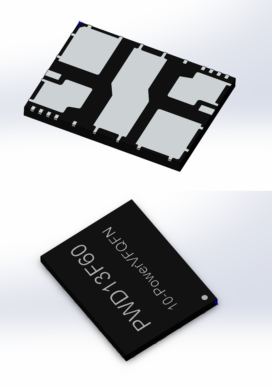
Before proceeding to reviewing the circuitry of my test board, I would like to save people who will use this module in the future from the enormous pain, namely the creation of a 3D model and a footprint. I attach the library components that I created during the design of the board - they are tested in a real piece of hardware and do not contain errors:
The body looks like this:
Now there are no obstacles for you to start using this module. Go to the circuitry. All the main nodes that can cause problems for the developer are already “hidden” inside the case and properly “prepared”, you just have to implement the control. By the way, this module allows you not only to create voltage converters, but also to control motors - this is another area of application, I think it will be very useful for fans of CNC machine tools and robotics.
The minimum piping required for the start: a pair of power capacitors, a pair of driver-step capacitors, and a PWM controller, in my case this is the STM32F410. Everything seems simple, but there is one, in my opinion, super important minus - there is no short circuit protection circuit inside the module! They are not what are not, but the emergency stop of drivers is not provided for. By the way, the TI module did not have its own short-circuit protection either. For me, the mystery is why it was impossible to shove another 2 comparators onto the crystal, which would measure the current on the external shunts and stop the driver ...
This disadvantage does not allow us to implement the highest-speed hardware protection against short-circuit. In any case, we will have to send a signal about the excess of current to the PWM controller and stop the operation by generating PWM. This significantly increases the response time of protection, and when using DSP or MK with the slightest “hanging” or delay, there will be an instant message.
Here you can go two ways - to hope for your smart code or to put between the PWM controller and the power module a logical buffer, which protection will disable. The second option is better, but it complicates the circuitry and still introduces an additional response delay, although it is significantly less than the work through DSP / MK. As it should be, I chose the bad option and naively hope for my “perfect” code. Firstly, it’s just a debug board to play around, so nothing depends on it and you can afford such liberty. Secondly, the code inside the MK I will have the simplest (PI controller + sine generation), so I can easily track all critical nodes. To do the same in a large full-scale project is unlikely to succeed, although it depends on the qualifications of the developer, but I definitely don’t.
I went along the standard way of building protection: shunt + op-amp + repeater. As a repeater, I used the 2nd channel of my OU. Here, by the way, one more minus - if your task is to make a super-compact solution, then the current protection nodes will take away precious space. As a result, I got such a simple scheme (I advise you to watch the PDF, clickable image):
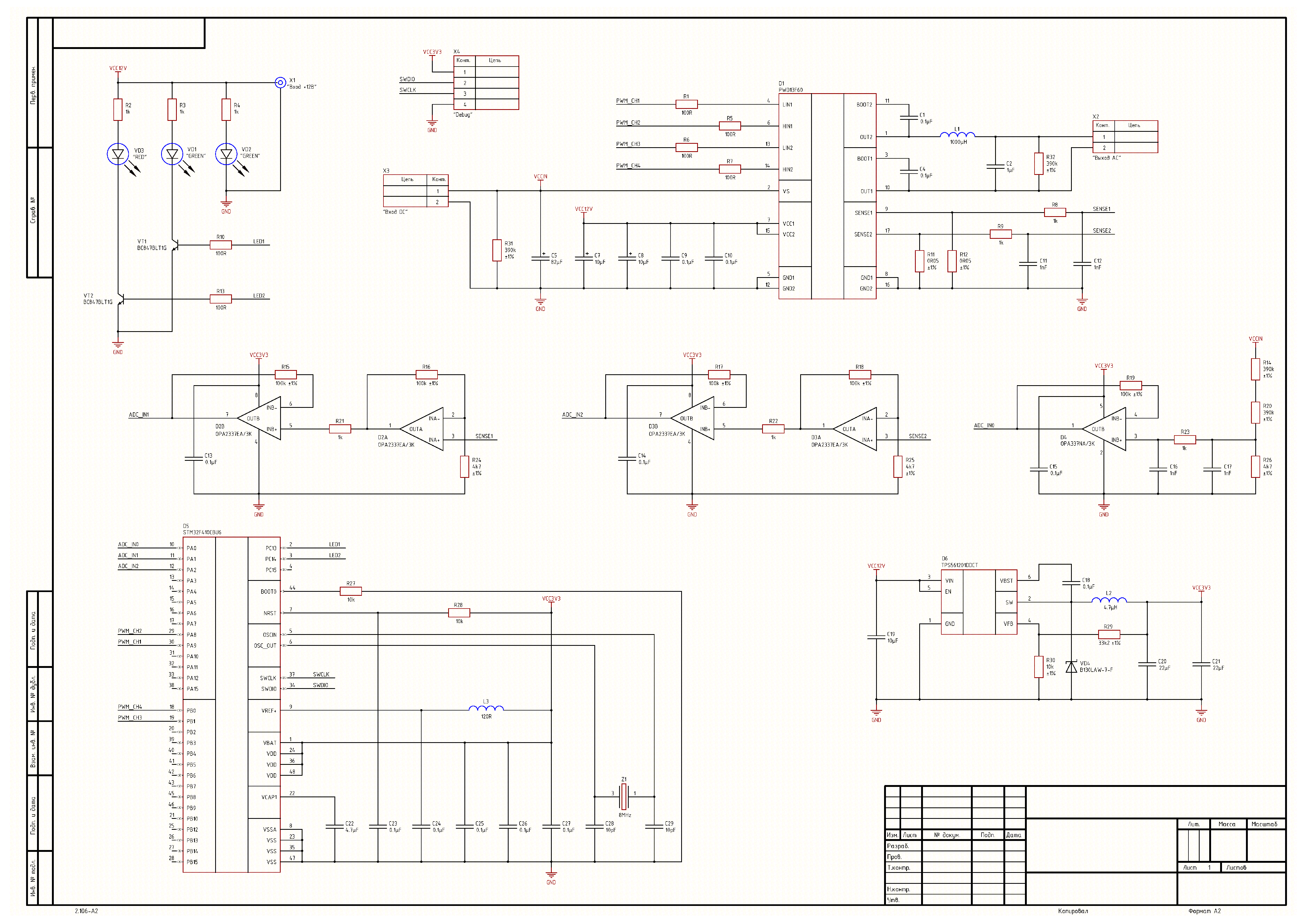
Since the device was made exclusively for the tests of this module, the scheme is continuous minimalism: STM32F410 + PWD13F60 + DC / DC microcontroller for powering the digital part + LC filter from the inductor and the 2.2 microfarad film + current protection + voltage OS. In general, everything. This scheme implements the conversion, for example, 310V from a rectified network, back to 220V. If you are a novice developer or a not very experienced amateur, then I strongly advise you to run in all the algorithms for 12-40V first and only then poke into the socket. This will allow you not to splurge on burnt modules and possibly survive.
Current protection implemented on dual op amps D2 and D3 - OPA2337. They are fast and allow you to implement the full operation of the OS chain at frequencies up to 400-600 kHz. The first half of the op-amp amplifies the signal from the shunt, and the second half works as a voltage follower.
As in the case of the scheme - the design of the PCB is open and available for review. Download PCB file for Altium Designer here . For a special masterpiece does not claim, because It was designed in a couple of hours, but the thermal calculations and modeling in basic form in Comsol were carried out - there will be no overheating, but a small aluminum radiator must still be installed on the module if you are going to remove more than 4-5A current. He also did basic calculations and modeling of parasitic inductances with subsequent optimization for their reduction. The dimensions of the printed circuit board turned out to be 100x45 mm , which is very good for a 1000 W converter, especially considering that there is no need for any intricacies or high frequencies.
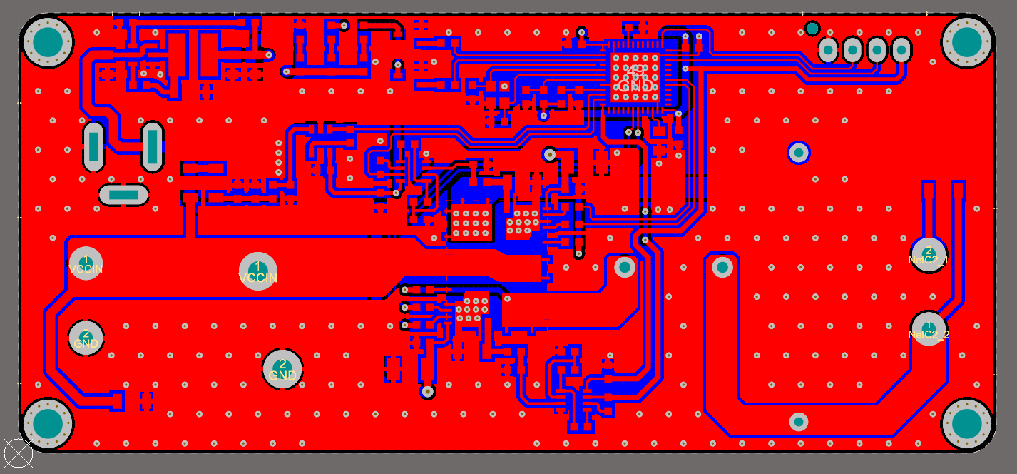
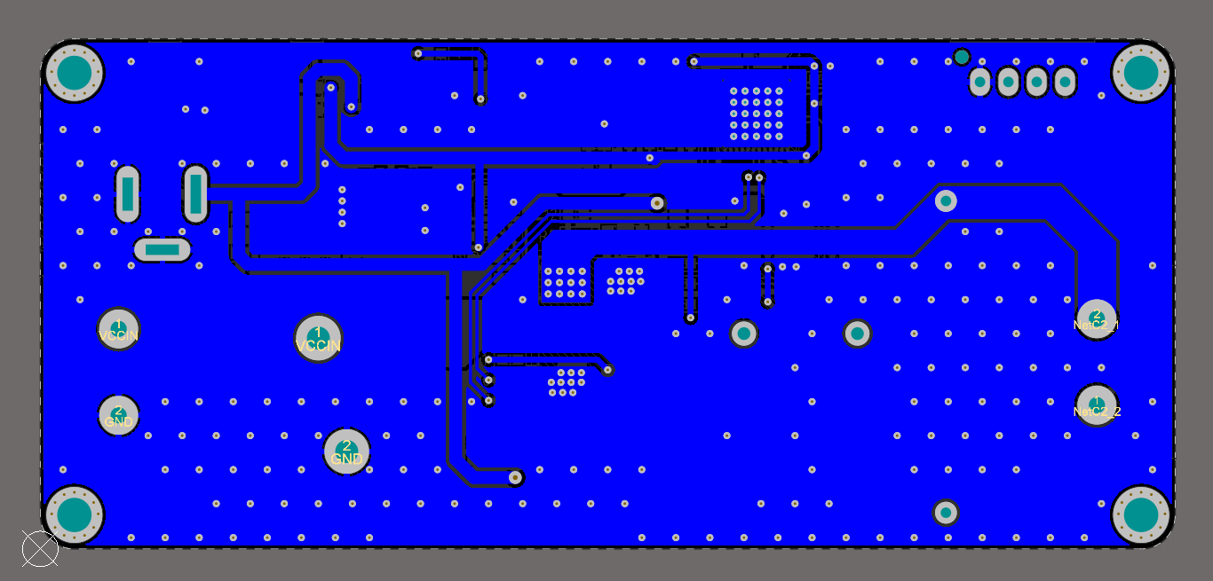

The board is double-layered, silk-screen printing and components only on the top layer. I ordered printed circuit boards on PCBway and they managed delivery by mail at $ 14 for 10 pieces:

I won’t say how much the components went, since I ordered for several different projects, but something around $ 20-25 of which $ 9 was the cost of the PWD13F60 module itself . I think you have already calculated the cost of 4 mosfet-s and 2 drivers for them and realized that this module is a very profitable solution.
Components ordered everything with Mouser via PM Electronics, carry quickly and without cheating, delivery by courier to the apartment is free, so I recommend. Who is interested in specific components - in the file with the scheme, each component has a part number registered and there is a link (move the mouse over the components and press F1, it will open).
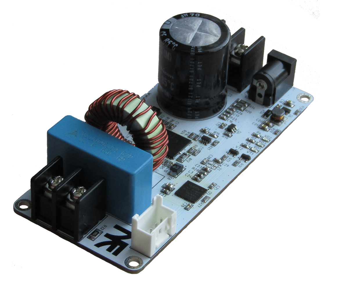
Separately say installation. I was a little worried about the PWD13F60 case, because The footprint itself was not run in and the possibility of a defect in soldering was embarrassing. I decided to solder not with a hairdryer, but in order for sure - in the stove. The flux from Ersa and a good paste from the People's Republic of China did their job - even with a not very neat installation, the microcircuit itself was centered by surface tension forces, the benefit of the guys from ST made the case completely symmetrical, albeit a complex shape. Since I was experimenting, I didn’t solder everything in the oven, so that if I killed a board, I wouldn’t have to rewire everything — I would solder PWD13F60, STM32F410 and the choke for dc / dc 12-3.3V in the furnace. The rest was soldered by a soldering iron and it turned out like this:
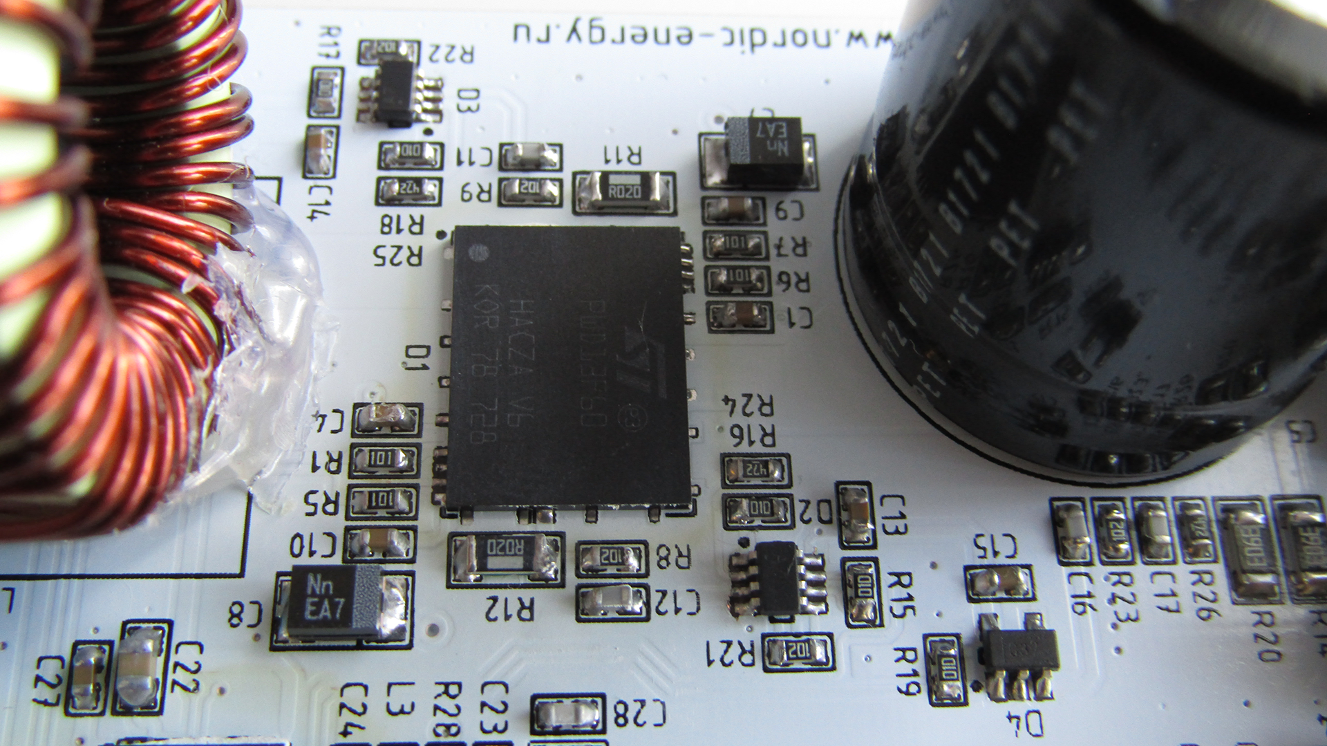
Here is a module turned out. For testing, we supply 12V from an external source, for example, a power supply unit from a router - the connector there is a standard 2.1 mm pin. Next, for the beginning, you can apply for the power input from the laboratory power supply unit about 20-30V and write the simplest code for the STM, pull the bridge and see what is at the output. If at idle everything is cold - good. We connect the load from the resistors to the output so that the current consumption is 1A and we look at the heating - the module must be slightly warm, the overheating is no more than 5 degrees. If this is the case, then we write the code to generate a sine, check it again for 20-30V, and only then you can apply rectified mains voltage. I advise you to initially apply voltage through a 40 W incandescent lamp into the break + VIN, if at idle everything is good, then add the same 40 W lamp to the output - does it work? Then remove the lamp from the entrance.
By the way, those who do not want to write code, I can buy the EG8010 microcircuit on Ali, namely the microcircuit, not the module, and get the same inverter without having to write the code for STM32. I think many fans of alternative energy will undoubtedly be pleased, because not everyone can and not everyone wants to write code on microcontrollers.
Here is an interesting module made in ST. I think it will be interesting to many, because saves us from many problems arising in the design of power electronics and allows us to obtain very small dimensions of the converter.
The proposed design of the board has already been tested, no problems have been found, everything is fine with spurious parameters, so it is interesting for anyone interested to study this module and power electronics as a whole, I recommend at least familiarizing yourself with it, and maybe repeating it without changes. By the way, I attach the archive with the project in Altium Designer - here .
In the next article I will adapt the code from the first article and we will implement a full-fledged DC / AC inverter, which can even be used in principle when building an inverter to work with solar panels or a wind generator.
A few weeks ago, one of my friends, knowing that I love power electronics, threw me a message that contained an advertising link from STMicroelectronics. In this link, the new solution from ST in the field of power electronics is described - PWD13F60. My very concept of "power electronics" is primarily associated with TI, Infineon, Linear, but not with ST. My view on ST, as a “power” manufacturer, fell for the first time when a magnificent controller came out - STSPIN32F0. The second time I looked right now.
PWD13F60 is a microcircuit, in a QFN-like package, which already contains a full bridge, that is, 4 high-voltage Mosfet, as well as drivers for them. The first idea came when I got acquainted with the datasheet: “Oh, yes, this is a kilowatt in my pocket!”, Hence the name of the article. I don’t really like various debugging boards and prefer to do some “combat” project right away. Based on the hero of this article, it was decided to make a DC / AC inverter.
I decided to divide the article into two parts: circuitry and code. Today I will tell about the circuit design solution, share libraries, design and first impressions. In the second part, we implement the management principles that were described in my first article.
Technical Specifications PWD13F60
The first thing you notice when reading this module is it is high voltage. There are not so many compact, integrated solutions for working with a single-phase network (220V AC / 310V DC). I came across a solution from TI based on GaN transistors - LMG3410, I really liked it, but unfortunately it hasn’t gone on the official sale yet and weighs about a year at the “preview” stage. Yes, the solution from TI is better in all parameters, but what's the use of it if the modules are not purchased? Alas, ah ... That's why I was so interested in the module from ST! Yes, it is on ordinary silicon, but it is a little less current, and yes at 1+ MHz it is unlikely that you can build anything, but this is not so bad and rather my nagging. Modern mosfet on silicon are closely matched to GaN, and the frequencies of 1+ MHz are still quite exotic: expensive and not very necessary.
Let's open the datasheet on PWD13F60 and get acquainted with its main characteristics:
- Drain-source voltage: 600V
- Open channel resistance: 0.32 ohm
- Maximum channel current (at 25 o C): 8A
- Maximum current channel (at 100 o C): 6.9A
- Maximum pulse current: 32A
- Logic Level Control: 3.3 and 5V
- Shutter charge: 26 nC
- Internal diode recovery time: 93 ns
Looking at the performance data you can draw a few conclusions. First, the voltage of 600V makes it possible to implement most of the topologies: full bridge, half bridge, LLC half bridge, phase-shifting bridge, and others. Secondly, the maximum channel current of 8A allows you to build a converter with a nominal power of 1000 watts. Thirdly, the channel resistance 320 mOhm is a good indicator, although it can be better. Fourthly, the gate capacitance and the speed of the technological diode make it possible to climb into the range 200-300 kHz even without the use of resonant topologies. Fifthly, the module can be controlled directly from the MK pins, which is very convenient and simplifies the circuit.
It turns out we have a very good module that allows you to solve many problems. It should be understood that 1000 W is achievable for a DC / AC converter, if you want a bridge DC / DC with a universal range of 85-265V, then you will not receive such power. When you enter 85V, you simply resist the maximum current and cooling of the crystal. You can definitely build a 300 W switching power supply with a universal input and extremely small dimensions.
Circuitry
Before proceeding to reviewing the circuitry of my test board, I would like to save people who will use this module in the future from the enormous pain, namely the creation of a 3D model and a footprint. I attach the library components that I created during the design of the board - they are tested in a real piece of hardware and do not contain errors:
The body looks like this:
Now there are no obstacles for you to start using this module. Go to the circuitry. All the main nodes that can cause problems for the developer are already “hidden” inside the case and properly “prepared”, you just have to implement the control. By the way, this module allows you not only to create voltage converters, but also to control motors - this is another area of application, I think it will be very useful for fans of CNC machine tools and robotics.
The minimum piping required for the start: a pair of power capacitors, a pair of driver-step capacitors, and a PWM controller, in my case this is the STM32F410. Everything seems simple, but there is one, in my opinion, super important minus - there is no short circuit protection circuit inside the module! They are not what are not, but the emergency stop of drivers is not provided for. By the way, the TI module did not have its own short-circuit protection either. For me, the mystery is why it was impossible to shove another 2 comparators onto the crystal, which would measure the current on the external shunts and stop the driver ...
This disadvantage does not allow us to implement the highest-speed hardware protection against short-circuit. In any case, we will have to send a signal about the excess of current to the PWM controller and stop the operation by generating PWM. This significantly increases the response time of protection, and when using DSP or MK with the slightest “hanging” or delay, there will be an instant message.
Here you can go two ways - to hope for your smart code or to put between the PWM controller and the power module a logical buffer, which protection will disable. The second option is better, but it complicates the circuitry and still introduces an additional response delay, although it is significantly less than the work through DSP / MK. As it should be, I chose the bad option and naively hope for my “perfect” code. Firstly, it’s just a debug board to play around, so nothing depends on it and you can afford such liberty. Secondly, the code inside the MK I will have the simplest (PI controller + sine generation), so I can easily track all critical nodes. To do the same in a large full-scale project is unlikely to succeed, although it depends on the qualifications of the developer, but I definitely don’t.
I went along the standard way of building protection: shunt + op-amp + repeater. As a repeater, I used the 2nd channel of my OU. Here, by the way, one more minus - if your task is to make a super-compact solution, then the current protection nodes will take away precious space. As a result, I got such a simple scheme (I advise you to watch the PDF, clickable image):
Since the device was made exclusively for the tests of this module, the scheme is continuous minimalism: STM32F410 + PWD13F60 + DC / DC microcontroller for powering the digital part + LC filter from the inductor and the 2.2 microfarad film + current protection + voltage OS. In general, everything. This scheme implements the conversion, for example, 310V from a rectified network, back to 220V. If you are a novice developer or a not very experienced amateur, then I strongly advise you to run in all the algorithms for 12-40V first and only then poke into the socket. This will allow you not to splurge on burnt modules and possibly survive.
Current protection implemented on dual op amps D2 and D3 - OPA2337. They are fast and allow you to implement the full operation of the OS chain at frequencies up to 400-600 kHz. The first half of the op-amp amplifies the signal from the shunt, and the second half works as a voltage follower.
Printed circuit board
As in the case of the scheme - the design of the PCB is open and available for review. Download PCB file for Altium Designer here . For a special masterpiece does not claim, because It was designed in a couple of hours, but the thermal calculations and modeling in basic form in Comsol were carried out - there will be no overheating, but a small aluminum radiator must still be installed on the module if you are going to remove more than 4-5A current. He also did basic calculations and modeling of parasitic inductances with subsequent optimization for their reduction. The dimensions of the printed circuit board turned out to be 100x45 mm , which is very good for a 1000 W converter, especially considering that there is no need for any intricacies or high frequencies.
The board is double-layered, silk-screen printing and components only on the top layer. I ordered printed circuit boards on PCBway and they managed delivery by mail at $ 14 for 10 pieces:
I won’t say how much the components went, since I ordered for several different projects, but something around $ 20-25 of which $ 9 was the cost of the PWD13F60 module itself . I think you have already calculated the cost of 4 mosfet-s and 2 drivers for them and realized that this module is a very profitable solution.
Components ordered everything with Mouser via PM Electronics, carry quickly and without cheating, delivery by courier to the apartment is free, so I recommend. Who is interested in specific components - in the file with the scheme, each component has a part number registered and there is a link (move the mouse over the components and press F1, it will open).
Separately say installation. I was a little worried about the PWD13F60 case, because The footprint itself was not run in and the possibility of a defect in soldering was embarrassing. I decided to solder not with a hairdryer, but in order for sure - in the stove. The flux from Ersa and a good paste from the People's Republic of China did their job - even with a not very neat installation, the microcircuit itself was centered by surface tension forces, the benefit of the guys from ST made the case completely symmetrical, albeit a complex shape. Since I was experimenting, I didn’t solder everything in the oven, so that if I killed a board, I wouldn’t have to rewire everything — I would solder PWD13F60, STM32F410 and the choke for dc / dc 12-3.3V in the furnace. The rest was soldered by a soldering iron and it turned out like this:
Here is a module turned out. For testing, we supply 12V from an external source, for example, a power supply unit from a router - the connector there is a standard 2.1 mm pin. Next, for the beginning, you can apply for the power input from the laboratory power supply unit about 20-30V and write the simplest code for the STM, pull the bridge and see what is at the output. If at idle everything is cold - good. We connect the load from the resistors to the output so that the current consumption is 1A and we look at the heating - the module must be slightly warm, the overheating is no more than 5 degrees. If this is the case, then we write the code to generate a sine, check it again for 20-30V, and only then you can apply rectified mains voltage. I advise you to initially apply voltage through a 40 W incandescent lamp into the break + VIN, if at idle everything is good, then add the same 40 W lamp to the output - does it work? Then remove the lamp from the entrance.
By the way, those who do not want to write code, I can buy the EG8010 microcircuit on Ali, namely the microcircuit, not the module, and get the same inverter without having to write the code for STM32. I think many fans of alternative energy will undoubtedly be pleased, because not everyone can and not everyone wants to write code on microcontrollers.
Total
Here is an interesting module made in ST. I think it will be interesting to many, because saves us from many problems arising in the design of power electronics and allows us to obtain very small dimensions of the converter.
The proposed design of the board has already been tested, no problems have been found, everything is fine with spurious parameters, so it is interesting for anyone interested to study this module and power electronics as a whole, I recommend at least familiarizing yourself with it, and maybe repeating it without changes. By the way, I attach the archive with the project in Altium Designer - here .
In the next article I will adapt the code from the first article and we will implement a full-fledged DC / AC inverter, which can even be used in principle when building an inverter to work with solar panels or a wind generator.