Stop putting diode

No, this is not just another “week-end”.
After reading the article on protection of electrical circuits against incorrect polarity of power supply using a field-effect transistor, I remembered that I have long had an unresolved problem of automatically disconnecting the battery from the charger when the latter is de-energized. And I became curious if it was possible to apply a similar approach in another case, where from time immemorial a diode was used as a locking element.
This article is a typical guide to cycling, because talks about the development of the scheme, the functionality of which has long been implemented in millions of ready-made devices. Therefore, the request does not refer to this material as to something completely utilitarian. Rather, it’s just a story about how an electronic device is born: from awareness of the need to a working prototype through all obstacles.
Why all this?
When reserving a low-voltage DC power source, the easiest way to turn on a lead-acid battery is as a buffer, just parallel to a network source, as was done in cars before they have complicated “brains”. Although the battery does not work in the most optimal mode, it is always charged and does not require any power switching when the mains voltage at the input power supply is turned off or on. Further more in detail about some problems of such inclusion and attempt to solve them.
Background
Some 20 years ago, this question was not on the agenda. The reason for this was the circuitry of a typical network power supply unit (or charger), which prevented the battery from discharging to its output circuits when the supply voltage was disconnected. Let's look at the simplest block diagram with half-wave straightening:

It is obvious that the same diode that rectifies the alternating voltage of the mains winding will also prevent the battery from discharging to the secondary winding of the transformer when the mains supply voltage is disconnected. The full-wave rectifier bridge circuit, despite somewhat less obvious, has exactly the same properties. And even the use of a parametric voltage regulator with a current amplifier (such as the widely used 7812 chip and its analogs) does not change the situation:

Indeed, if you look at the simplified circuit of such a stabilizer, it becomes clear that the emitter junction of the output transistor plays the role of the same diode, which closes when the voltage at the output of the rectifier is lost, and keeps the battery charge safe and sound.
However, in recent years, everything has changed. The transformer power supply units with parametric stabilization were replaced by more compact and cheap pulsed AC / DC voltage converters, which have much higher efficiency and a power / weight ratio. But with all the advantages, these power sources showed one drawback: their output circuits have a much more complicated circuit design, which usually doesn’t provide protection against reverse flow of current from the secondary circuit. As a result, when using such a source in the system of the “BP -> buffer battery -> load”, when the mains voltage is disconnected, the battery begins to discharge rapidly to the output power supply circuit.
The easiest way (diode)
The simplest solution is to use a Schottky barrier diode included in the break of the positive wire connecting the power supply and battery:
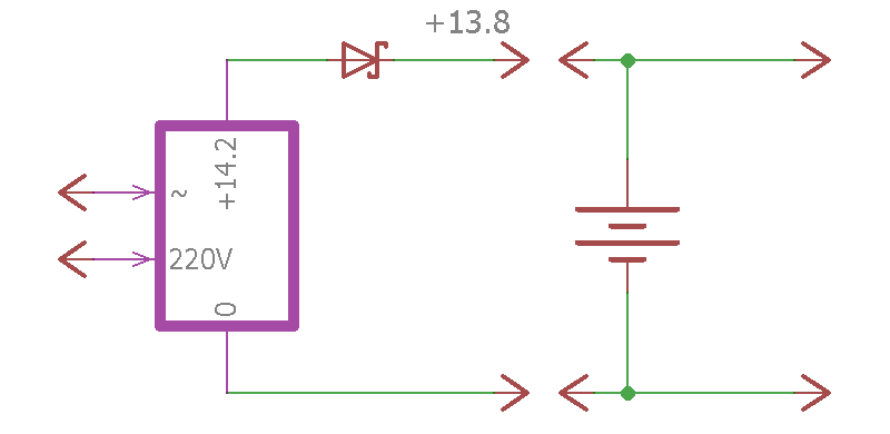
However, the main problems of this solution are already mentioned in the article mentioned above. In addition, this approach may be unacceptable for the reason that a 12-volt lead-acid battery needs at least 13.6 volts to work in a buffer mode. And almost half a volt falling on a diode can make this voltage unattainable in combination with an existing power supply (just my case).
All this forces us to look for alternative ways of automatic switching, which should have the following properties:
- Small forward voltage drop in the on state.
- The ability, without significant heating, to withstand in the switched on state the direct current consumed from the power supply unit by the load and the buffer battery.
- High reverse voltage drop and low self consumption when off.
- Normally off state, so that when a charged battery is connected to an initially de-energized system, its discharge does not begin.
- Automatic transition to the on state when the mains voltage is applied regardless of the presence and charge level of the battery.
- The fastest automatic transition to the off state in case of mains voltage drop.
If the diode were an ideal device, it would have fulfilled all these conditions without any problems, however, the harsh reality calls into question points 1 and 2.
Naive solution (DC relay)
When analyzing the requirements, anyone who is even slightly “in the subject” will come up with the idea to use for this purpose an electromagnetic relay that is able to physically close the contacts using a magnetic field created by the control current in the winding. And, probably, he even writes something like this on a napkin:
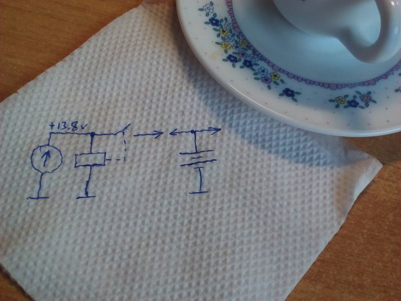
In this scheme, normally open contacts of the relay are closed only when current passes through a winding connected to the output of the power supply. However, if you go through the list of requirements, it turns out that this scheme does not correspond to item 6. If the relay contacts were once closed, the loss of the mains voltage will not lead to their opening for the reason that the winding (and with it the entire output power supply circuit) remains connected to the battery through the same contacts! There is a typical case of positive feedback, when the control circuit has a direct connection with the executive one, and as a result, the system acquires the properties of a bistable trigger.
Thus, such a naive approach is not a solution to the problem. Moreover, if we analyze the current situation logically, it is easy to come to the conclusion that in the interval “BP -> backup battery” in ideal conditions, no other solution other than a valve that conducts current in one direction can simply not be. Indeed, if we do not use any external control signal, then whatever we do at this point of the circuit, any of our switching element, once turned on, will make the electricity generated by the battery indistinguishable from the electricity generated by the power supply.
Circumstance (AC Relay)
After understanding all the problems of the previous paragraph, a “rummaging” person usually comes up with a new idea of using the power supply itself as a one-way conductive valve. Why not? After all, if a power supply unit is not a reversible device, and the battery voltage supplied to its output does not generate 220 volts AC input (as is the case in 100% of real circuits), then this difference can be used as a control signal for the switching element:
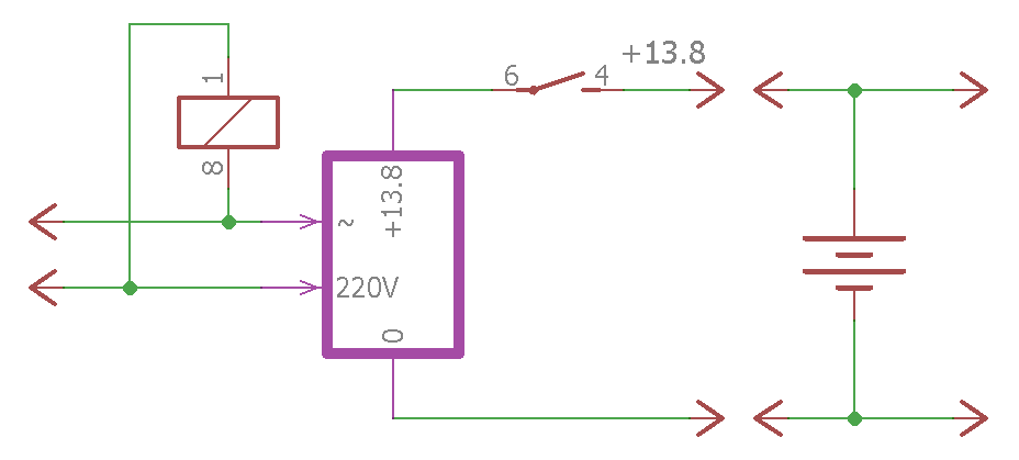
Bingo! All clauses of the requirements are fulfilled and the only thing needed for this is a relay capable of closing the contacts when the mains voltage is applied to it. This may be a special AC relay rated for line voltage. Or an ordinary relay with its own mini-PSU (there is enough of any transformerless step-down circuit with the simplest rectifier).
It would be possible to celebrate the victory, but I did not like this decision. First, you need to connect something directly to the network, which is not good from a security point of view. Secondly, by the fact that this relay must switch significant currents, probably up to tens of amperes, and this makes the whole structure not as trivial and compact as it might have initially seemed. And thirdly, what about such a convenient field effect transistor?
Первое решение (полевой транзистор + измеритель напряжения аккумулятора)
The search for a more elegant solution to the problem led me to the realization that the battery, operating in buffer mode at a voltage of about 13.8 volts, without external “recharge” quickly loses the original voltage even in the absence of a load. If it starts discharging to the power supply unit, then in the first minute of time it loses at least 0.1 volts, which is more than enough for reliable fixation with the simplest comparator. In general, the idea is this: the gate of the switching field-effect transistor is controlled by a comparator. One of the inputs of the comparator is connected to a source of stable voltage. The second input is connected to the voltage divider of the power supply. Moreover, the division ratio is chosen so that the voltage at the output of the divider when the power supply is turned on is approximately 0.1.0.0 volts higher than the voltage of the stabilized source. As a result When the power supply unit is turned on, the voltage from the divider will always prevail, but when the network is de-energized, as the battery voltage drops, it will decrease in proportion to this drop. After some time, the voltage at the output of the divider will be less than the voltage of the stabilizer and the comparator will break the circuit using the field-effect transistor.
An approximate diagram of such a device:
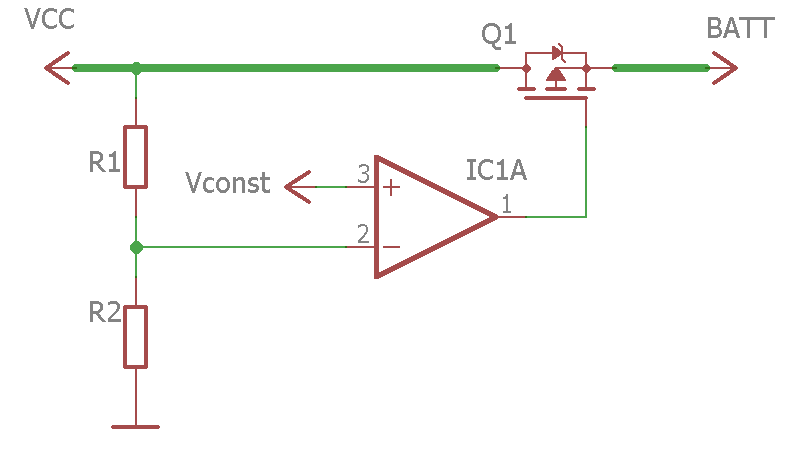
As can be seen, a direct input of the comparator is connected to a source of stable voltage. The voltage of this source, in principle, is not important; the main thing is that it is within the allowable input voltages of the comparator, however, it is convenient when it is about half the battery voltage, that is, about 6 volts. The inverse input of the comparator is connected to the voltage divider of the power supply unit, and the output is connected to the gate of the switching transistor. When the voltage at the inverted input exceeds that on the direct one, the output of the comparator connects the gate of the field-effect transistor to the ground, with the result that the transistor opens and closes the circuit. After de-energizing the network, after some time the battery voltage drops, along with it the voltage drops at the comparator's inverted input, and when it falls below the level at the direct input, the comparator "tears off" the transistor gate from the ground and thus breaks the circuit. Later, when the power supply unit comes to life again, the voltage at the inverse input instantly rises to the normal level and the transistor opens again.
For the practical implementation of this scheme I used the LM393 chip that I had. It is very cheap (less than ten cents in retail), but at the same time economical and has a fairly good performance dual comparator. It allows power up to 36 volts, has a transmission coefficient of at least 50 V / mV, and its inputs have a rather high impedance. The first commercially available high-power P-channel MOSFETs FDD6685 was taken as the switching transistor. After several experiments, the following switch circuit was developed:

In it, an abstract source of stable voltage is replaced by a completely real parametric stabilizer of resistor R2 and Zener diode D1, and the divider is made on the basis of a trimming resistor R1, which allows to adjust the division factor to the desired value. Since the comparator inputs have a very significant impedance, the value of the damping resistance in the stabilizer can be more than a hundred kΩ, which allows minimizing the leakage current, and hence the total consumption of the device. The nominal value of the trimmer resistor is generally not critical and without any consequences for the performance of the circuit can be selected in the range from ten to several hundred kΩ. Due to the fact that the output circuit of the LM393 comparator is built according to the open-collector circuit, a load resistor R3 is also required for its functional completion,
The adjustment of the device is reduced to setting the position of the trimmer resistor in a position in which the voltage on the leg 2 of the chip is higher than that on the leg 3 by about 0.1..0.2 volts. To set up, it is better not to use a multimeter in a high-impedance circuit, but simply setting the resistor slider to the lower (according to the diagram) position, connect the PSU (we do not connect the battery yet), and measuring the voltage at pin 1 of the microcircuit, move the resistor contact upwards. As soon as the voltage drops abruptly to zero, the pre-setting can be considered complete.
You should not strive to turn off with a minimum voltage difference, because this will inevitably lead to incorrect operation of the circuit. In reality, on the contrary, it is necessary to specifically reduce the sensitivity. The fact is that when switching on the load, the voltage at the input of the circuit inevitably subsides due to the non-perfect stabilization in the power supply and the final resistance of the connecting wires. This may result in an overly sensitive device considering such a drawdown as a power off and breaking the circuit. As a result, the PSU will be connected only when there is no load, and the rest of the time will have to work the battery. However, when the battery is slightly discharged, the internal diode of the field-effect transistor will open and the current from the power supply will begin to flow into the circuit through it. But this will cause the transistor to overheat and That the battery will work in the mode of a long undercharging. In general, the final calibration should be carried out under real load, controlling the voltage at pin 1 of the chip and, as a result, leaving a small margin for reliability.
As a result of practical tests such results were obtained. Resistance in the open state corresponds to the resistance of the datasheet to the transistor. In the closed state, the parasitic current in the secondary power supply circuit could not be measured due to its insignificance. The current consumption in the battery mode was 1.1 mA, and it is almost 100% composed of the current consumed by the chip. After calibration under the maximum load, the response time without load was almost 15 minutes. It took so much time for my battery to discharge to the voltage that comes from the power supply unit to the device under full load. True, shutdown at full load occurs almost immediately (less than 10 seconds), but this time depends on the capacity, charge, and the overall "health" of the battery.
Significant disadvantages of this scheme are the relative complexity of calibration and the need to put up with the potential loss of battery energy for the sake of correct operation.
The last drawback did not give rest, and after some deliberation I was led to the idea of measuring not the battery voltage, but the actual direction of the current in the circuit.
Second solution (field effect transistor + current direction meter)
To measure the direction of the current could use some tricky sensor. For example, a Hall sensor that registers a magnetic field vector around a conductor and allows us to determine not only the direction but also the current strength without breaking the circuit. However, due to the absence of such a sensor (and experience with similar devices), it was decided to try to measure the sign of the voltage drop on the field-effect transistor. Of course, in the open state, the channel resistance is measured in hundredths of an ohm (for the sake of this and the whole undertaking), but, nevertheless, it is certainly possible and you can try to play with it. An additional argument in favor of this decision is the lack of need for fine adjustment. We will only measure the polarity of the voltage drop, not its absolute value.
According to the most pessimistic calculations, when the open channel resistance of the FDD6685 is about 14 mΩ and the differential sensitivity of the LM393 comparator from the “min” column is 50 V / mV, we will have at the output of the comparator a full voltage swing of 12 volts at a current through the transistor of just over 17 mA. As you can see, the value is quite real. In practice, it should be about an order of magnitude less, because the typical sensitivity of our comparator is 200 V / mV, the resistance of the transistor channel in real conditions, taking into account the installation, is unlikely to be less than 25 mΩ, and the range of the control voltage at the gate may not exceed three volt.
An abstract implementation will look something like this:

Here the comparator inputs are connected directly to the positive bus on opposite sides of the field-effect transistor. When current passes through it in different directions, the voltages at the inputs of the comparator will inevitably differ, and the sign of the difference will correspond to the direction of the current, and the magnitude will be its strength.
At first glance, the circuit is extremely simple, but there is a problem with the power supply of the comparator. It lies in the fact that we can not power the microcircuit directly from the same circuits that it should measure. According to the datasheet, the maximum voltage at the inputs of the LM393 should not be higher than the supply voltage minus two volts. If this threshold is exceeded, the comparator stops noticing the voltage difference at the direct and inverse inputs.
There are two potential solutions to this problem. The first, obvious, is to increase the voltage of the comparator. The second, which comes to mind, if you think a little, is to equally lower the control voltages with the help of two dividers. Here is what it might look like:

This scheme impresses with its simplicity and brevity, but in the real world, unfortunately, it is not realizable. The fact is that we are dealing with the voltage difference between the comparator inputs of just a millivolt. At the same time, the spread of resistances of resistors of even the highest accuracy class is 0.1%. With a minimum acceptable division ratio of 2 to 8 and a reasonable impedance of the divider of 10 kΩ, the measurement error will reach 3 mV, which is several times higher than the voltage drop across the transistor at a current of 17 mA. The use of a “trimmer” in one of the dividers is eliminated for the same reason, because selecting its resistance with an accuracy of more than 0.01% is not possible even when using a precision multi-turn resistor (plus we don’t forget about the time and temperature drift). In addition, as already stated above,
Based on all the above, in practice there remains only the option of increasing the supply voltage. In principle, this is not such a problem, considering that there is a huge number of specialized microcircuits, which allow using a few details to build a stepup converter at the desired voltage. But then the complexity of the device and its consumption will almost double, which I would like to avoid.
There are several ways to build a low-power boost converter. For example, most integrated transducers assume the use of a self-induction voltage of a small choke connected in series with a “power” switch located directly on the chip. Such an approach is justified with a relatively powerful conversion, for example, to supply the LED with a current of tens of milliamperes. In our case, this is clearly redundant, because you need to provide a current of only about one milliampere. We are much more suited to doubling the DC voltage with a control key, two capacitors, and two diodes. The principle of its operation can be understood by the scheme:
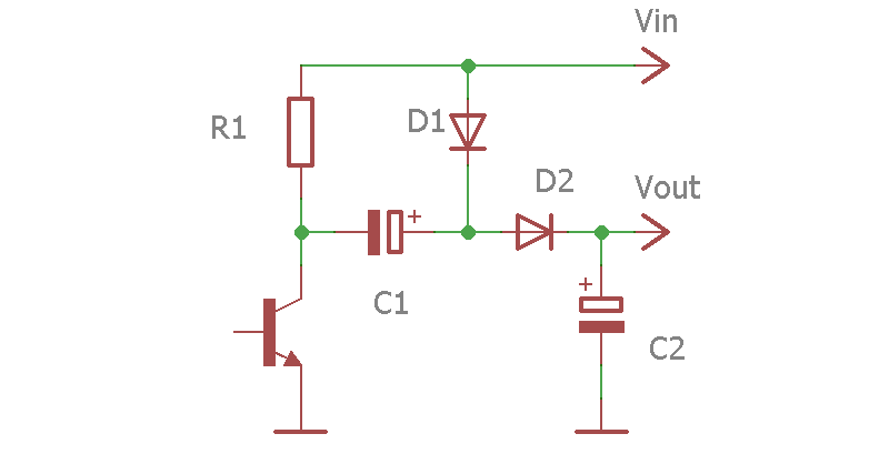
At the first moment of time when the transistor is closed, nothing interesting happens. The current from the power bus through the diodes D1 and D2 reaches the output, as a result of which even a slightly lower voltage is set at the capacitor C2 than that supplied to the input. However, if the transistor opens, capacitor C1 through diode D1 and the transistor will charge almost to the supply voltage (minus the direct drop on D1 and the transistor). Now, if we close the transistor again, it turns out that the charged capacitor C1 is connected in series with the resistor R1 and the power source. As a result, its voltage will add up with the voltage of the power source and, having suffered some losses in the resistor R1 and the diode D2, will charge C2 to almost double Uin. After that, the whole cycle can begin again. As a result, if the transistor switches regularly, and the energy output from C2 is not too large,
To implement such a doubler, in addition to the elements already listed, we need an oscillator and the key itself. It may seem that this is a lot of details, but in fact it is not, because we already have almost everything that is needed. I hope you have not forgotten that the LM393 contains in its composition two comparators? And what we used so far only one of them? After all, a comparator is also an amplifier, which means that if we cover it with positive feedback on alternating current, it will turn into a generator. In this case, its output transistor will regularly open and close, perfectly performing the role of the doubler key. Here's what we can do when trying to realize our plans:

At first, the idea of supplying a generator with voltage, which he himself actually produces during operation, may seem rather wild. However, if you take a closer look, you can see that the generator is initially powered through diodes D1 and D2, which is enough for it to start. After generation occurs, the doubler begins to work, and the supply voltage gradually rises to about 20 volts. This process takes no more than a second, after which the generator, and with it the first comparator, receives power, much higher than the operating voltage of the circuit. This gives us the opportunity to directly measure the voltage difference at the source and drain of the field-effect transistor and achieve our goal.
Here is the final diagram of our switch:

There is nothing to explain about it, everything is described above. As you can see, the device does not contain any adjusting element and, if properly assembled, it starts working immediately. In addition to the already familiar active elements, only two diodes were added, as which you can use any low-power diodes with a maximum reverse voltage of at least 25 volts and a maximum forward current of 10 mA (for example, the widespread 1N4148 that can be evaporated from the old motherboard).
This scheme was tested on a breadboard, where it proved its full working capacity. The resulting parameters are fully consistent with the expectations: instantaneous switching in both directions, the absence of inadequate response when the load is connected, the current consumption from the battery is only 2.1 mA.
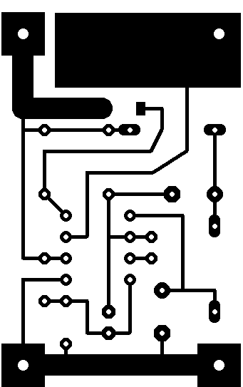
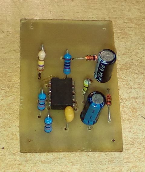
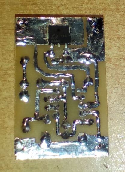
One of the options for PCB layout is also attached. 300 dpi, view from the side of the parts (so you need to print in mirror image). The field-effect transistor is mounted on the side of the conductors. Assembled device, completely ready for installation: Diluted in the old-fashioned way, so it turned out a bit crooked, but nevertheless the device has been regularly performing its functions in a circuit with a current of up to 15 amperes without any signs of overheating. Archive with schematic and layout files for EAGLE . Thanks for attention.