We make a scintillation radiometer ourselves. Part 1, hardware
In a previous article, I showed a little in my work a homemade scintillation radiometer. The device has interested the public and in connection with this comes out this article describing the radiometer from the inside.
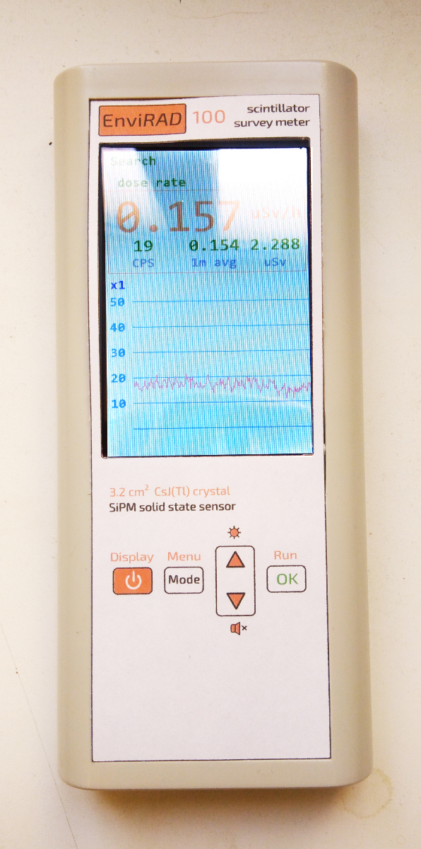
The vast majority of pocket-sized dosimeters and radiometers are instruments based on a Geiger counter. This type of detector has its advantages, the main of which are simplicity and low cost, but also a number of disadvantages. First of all, this is a very low efficiency of gamma-ray registration and a complete lack of information about their energy. A Geiger counter captures only one gamma-ray of several hundred, while a low-energy scintillation detector provides almost 100% efficiency. As a result, with a natural background with the same dimensions of the detectors, when the Geiger counter gives only 10-15 pulses per minute, the scintillator gives the same number of pulses, but per second. Thus, in order to get at least some idea of the dose rate, we must spend at least a minute on a set of pulses with a Geiger counter, and with a scintillator we can receive information about the radiation situation every second. So the scintillation detector gives us, first of all, the speed of reaction to weak sources of radioactivity.
In addition, the scintillation detector has the property of proportionality. The higher the particle energy, the greater the amplitude of the pulse at the detector output. What is it for? First, this is how we get information about what is the source of radiation. Each radioactive isotope has its own characteristic energy of gamma radiation (or a set of energies). The gamma spectrometry method is based on this. In this device, the average absorbed energy per quantum will be displayed on the screen (not yet done).
Secondly, if we simply count impulses without taking into account energy, we get an unpleasant thing called “a move with rigidity”. Suppose we calibrated our cesium-137 radiometer. And then they were in a place infected with americium-241. The energy of the cesium-137 quantum is 667 keV, America - 59 keV, that is, more than an order of magnitude less. So, with the same number of particles trapped by the detector (and, therefore, with the same readings from the device), the absorbed dose will be more than an order of magnitude less. That is, the measurements will be erroneous. And in order for the radiometer to measure the dose correctly at different energies (that is, to be a dosimeter ), the energy of each registered quantum must be taken into account.
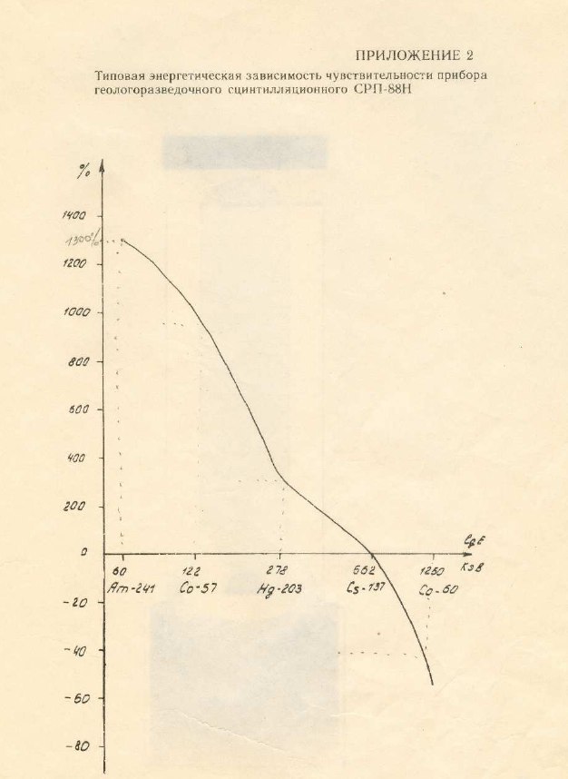
Portable scintillation radiometers-dosimeters have been on the market for a long time. But for the most part these are very expensive devices for professional use. I know of only one device, oriented to home and amateur use - this is Atom Fast manufactured by KB Radar. The rest - Polimaster devices, a number of foreign companies - are very expensive.
In this device I wanted to get the following:
As a result, the described device was obtained. It is not finished yet, there is still enough work, especially with software.
The radiometer operates in one of two modes: search and measurement. In the search mode, the readings of the device are updated every second, while in addition to the readings in digital form, they are displayed in a graph. In the search mode, no attention is paid to errors; in this mode, the device is primarily an indicator. The screen displays: current dose rate, count rate in pulses per second (CPS), as well as the dose rate averaged over the last minute and the integral dose accumulated after the device was turned on or after a reset. In the measuring mode, on the contrary, the measurement time is set by the operator (by pressing the “Enter” button to start and then to end the measurement), and the calculated error is displayed on the screen along with the measured value, and a mini-journal of the last few is displayed in its “basement” measurements. Moreover, in the measuring mode, the first attempt was made to take into account the energy of quanta and compensate for the “stroke with rigidity”. The measuring mode is in deep under construction and it is not yet in the given firmware version.
Regardless of the mode, the second-second cycle of measurements continues, with the results being saved to RAM. In particular, due to this, when switching to the search mode, the graph displays the readings that were during the stay of the device in the measurement mode, as well as during menu entries, etc. Regardless of the mode, the alarm for exceeding thresholds also works.
There are three thresholds in the latter. The traditional first and second - are set through the menu at the request of the operator and when they are triggered by the results of the next second counting cycle, a sound signal sounds. In addition to them, there is also an adaptive threshold. It is automatically set at an average level per minute, setting at one, two or three sigma (you can select in the settings) from it. If an operation on this threshold occurs in the next cycle, the value from the previous cycle is taken for the next cycle, so that with a slow but steady increase in radiation, a stable alarm is achieved. Subsequently, a log of alarms will be implemented, but so far it is not.
It has not yet been implemented to save the measurement results to a microSD card, the connector for which is mounted on the radiometer board. It also provides for the connection of a GPS module, the use of which is also a matter of the future.
Switching modes and quick change of some settings is done through the "hot keys", the rest of the operations - using the menu. Entering the menu, as already mentioned, does not stop the measurement process.
The radiometer is mounted in a standard Chip-and-Dip case Gainta G1389G measuring 122x77x25 mm. On the upper panel there is a 3.5 ”color LCD with a resolution of 480x320 pixels. The display uses the Nextion NX4832T035 HMI module, which differs from conventional displays by its own microcontroller, which contains a ready-made program for displaying interface elements, but we just need to send commands to display them, remove or change them - for example, change one or another digit, draw another point on the chart or change the color of one or another inscription. Under the display is a keyboard of five buttons. There is space left for the GNSS receiver, and a scintillation detector is located at the upper end.
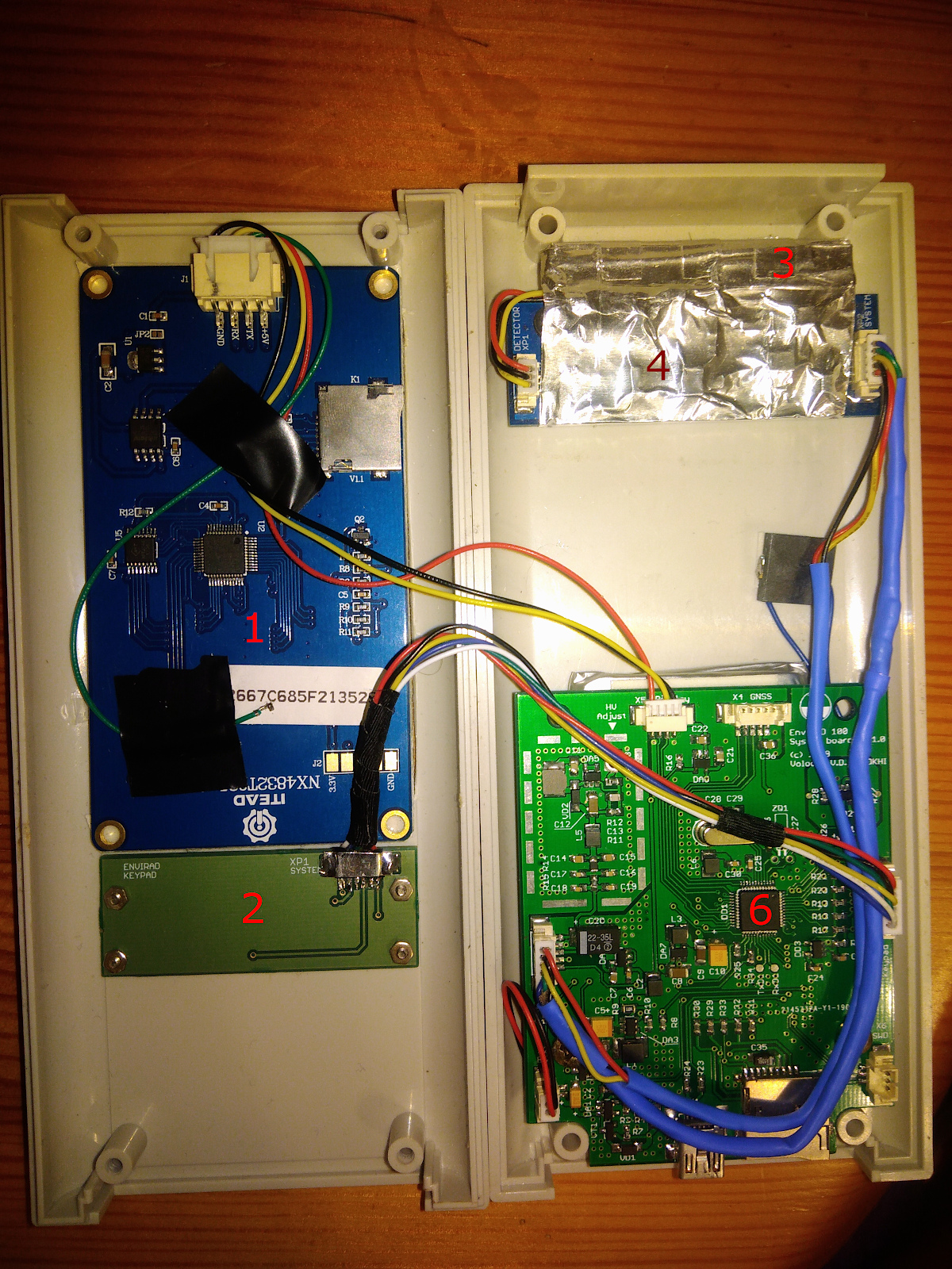
Red numbers indicate: 1 - display module, 2 - keyboard, 3 - detector, 4 - analog board, 6 - system board.
The electronic circuit of the device (not counting the display and the navigation receiver, as well as the keyboard) is assembled on two printed circuit boards. On the first, the analog part of the device is assembled, on the second - everything else: a microcontroller with a strapping, a power circuit and its switching, battery charging and a high voltage source for the detector.
A thallium activated scintillation crystal of cesium iodide is used as a detector in the radiometer. This crystal has the property of radioluminescence - charged particles and high-energy photons (X-ray and gamma range) excite a glow in it, and light is emitted in the form of a short, about a microsecond, flash of light - scintillation. This flash is too weak to be seen with the eye or detected in the usual way. Photocells, photodiodes and photoresistors are too insensitive for this. To assess the scale of the disaster, I will cite the following figures.
A gamma ray with an energy of 1 MeV, completely absorbed in a CsI (Tl) crystal, generates approximately 40,000 photons of green light. Let us try to catch this light with a photodiode. Suppose they all get on a photodiode (in fact, this is unrealistic and good if only half of them get on it). And let's say that we have an ideal photodiode, with a quantum output of 100%. This means that each of the photons will create one electron-hole pair in the structure of the photodiode. And for the momentum we get 40,000 photoelectrons. And this pulse lasts, as we know, 1 μs. So, in a second we will have 4 ∙ 10 10 photoelectrons. The electron charge is 1.6 ∙ 10 -19 C, and the charge 4 ∙ 10 10 photoelectrons is 6.4 ∙ 10 -9Kl, that is, the current strength that the scintillation flash will cause in our photodiode is just a few nanoamps! And if you remember that not all photons also get on the photodiode, and its quantum yield is not 100% ... And besides, the megaelectron-volt is the energy of rather hard gamma radiation, and it would be nice to see much lower energies. In general, photodiodes are practically not suitable for us here. Rather, they are suitable - but with great difficulty.
Usually photoelectronic multipliers were used (and are now used) to capture such weak pulses of light. In them, each photoelectron knocked out of the photocathode multiplies on the dynode system, giving a gain of millions of times, and the current pulse at its anode is no longer nano, but milliamperes, and registering such a pulse is no longer difficult. But PMTs are a solid size fragile glass cylinder, these are kilovolts of power, which in addition require high stability. In general, it is poorly represented in a pocket-sized device.
Fortunately, semiconductor photodetectors are now available that can compete in sensitivity with PMTs. Who said avalanche photodiodes? Yes, it's almost them. Only avalanche diodes, although they have an internal photocurrent gain due to the avalanche multiplication of carriers, have a number of technological problems that do not allow making a sensitive area with a diameter of at least a few millimeters. In addition, the classic avalanche diode has an avalanche amplification coefficient without complex tricks of only 10-200, which is minuscule compared to the million-fold amplification characteristic of a PMT. All these disadvantages of the avalanche photodiode are eliminated in the recently appeared on the market Si-PMT or SiPM. They are essentially a matrix of many avalanche photodiodes operating in pre-breakdown mode, in which a single photon is capable of provoking the development of avalanche breakdown. This mode is similar to the operation of the Geiger counter. Each of the cells has its own blanking scheme, due to which the avalanche breakdown immediately ceases and the cell becomes again ready to register a new photon. All cells (with their quenching schemes) are connected in parallel on a Si-PMT crystal, and the current pulses flowing through them are summed, so that the average current is proportional to the illumination of the crystal. And it is very simple to use such a silicon PMT - it is enough to apply a reverse bias to it - about 28-29 V through a resistor of several kilo-ohms, from which the signal can be taken. Nothing more is needed - neither a kilovolt power source, nor a divider for dynodes. And the Si-PMT itself is a small silicon square measuring 3x3 or 6x6 mm. By the way

So, our detector uses Si-PMTs and a CsI (Tl) crystal, between which a layer of optical lubricant is applied to eliminate the air gap between the crystal and the photodetector window. And on top of the crystal and Si-PMT are covered with many layers of a thin fluoroplastic film, known as FUM tape. This coating has a very high diffuse reflectance. The detector is covered with aluminum tape on top, providing protection from external light and sealing - the cesium iodide crystal is extremely soluble in water and the smallest trace of moisture entering the detector would destroy it. Fortunately, unlike its "relative" - sodium iodide, CsI practically does not have the property of hygroscopicity - that is, it does not attract moisture from the air. Sodium iodide crystals have to be processed only in an absolutely dry inert gas environment and placed in such high-sealed containers as if it would be necessary to create an ultrahigh vacuum in them, and in ordinary air they just blur before our eyes. And vice versa, cesium iodide in the form of single crystals can be easily treated in air (for example, sawed with an ordinary hacksaw for metal and sanded with a sandpaper), avoiding only traces of liquid water and remembering that the crystal contains extremely toxic thallium. However, due to the smallness of its amount, acute (but not chronic!) Toxicity will be determined by iodine, not thallium. Cesium iodide in the form of single crystals can be easily treated in air (for example, sawed with an ordinary hacksaw for metal and sanded with a sandpaper), avoiding only traces of liquid water and remembering that the crystal contains extremely toxic thallium. However, due to the smallness of its amount, acute (but not chronic!) Toxicity will be determined by iodine, not thallium. Cesium iodide in the form of single crystals can be easily treated in air (for example, sawed with an ordinary hacksaw for metal and sanded with a sandpaper), avoiding only traces of liquid water and remembering that the crystal contains extremely toxic thallium. However, due to the smallness of its amount, acute (but not chronic!) Toxicity will be determined by iodine, not thallium.
I will not give advice on the independent manufacture of the detector, since I did not deal with it (the finished detector was kindly provided to me by their developer and manufacturer KBRadarin exchange for some valuable artifacts for electronic engineers), I will give only its parameters. They are: the size of the crystal is 8x8x50 mm, and the Si-PMT MicroFC 30035 of the Irish company SensL (now it is an On Semi division) as a photodetector. A variety of manufacturing tips can be found online. With a slight increase in size, you can take a standard CsI (Tl) or NaI (Tl) crystal in a “native” package of small sizes (10x40, 18x30 mm, etc.). True, the larger the size of the output window, the worse the photodetector with a size of 3x3 mm will work, so I strongly recommend taking a larger (and much more expensive) MicroFC 60035 with the diameter of the output window larger. By the way, the Broadcom analogs of these photodetectors are not recommended to use.

Its scheme is shown in the figure above. It consists of the following main nodes:
The detector is connected to the XP1 input connector. The Si-PMT cathode - to pin 3 (HV), the anode - to pin 1 (DET), and to the pin 2 (GND) the metal screen of the detector is connected - its wrapper is made of aluminum adhesive tape.
The input circuit consists of the load resistance of detector R2 and current-limiting resistance R1, which will try to protect the detector in case of trouble such as accidentally supplying too high a reverse bias voltage or incorrectly supplying a voltage of reverse polarity instead, if the detector itself is connected incorrectly. Together with the capacitance of a silicon PMT (approximately 900 pF), they form voltage pulses with a rise time of about 1 μs and a fall time of about 15 μs. Before applying to the input of the comparator, the signal is passed through a 470 pF capacitor, which decouples the circuit by direct current and, together with the input resistance of the divider R3R5R6, shortens the pulse to 2-3 μs.
An LMV7239 microcircuit was used as a comparator, combining low power consumption with sufficiently high speed (<100 ns) at low differential input voltages. The voltage divider R3R5R6 together with the integrating circuit R4C3 form a “floating” threshold voltage, making the comparator somewhat insensitive to the dark current of the detector and changes in the input current with temperature. The sensitivity of the comparator is controlled by the selection of resistance R5 in the range of several tens of Ohms. A rectangular pulse of negative polarity is formed at the output of the comparator. The trailing edge of this pulse may rattle slightly due to detector noise, but an attempt to get rid of this bounce by introducing hysteresis has led to a decrease in sensitivity and, in general, worse results.
A single-shot on the DA2 integrated timer (LMC555CM, in fact - a conventional 555 timer, only in CMOS version) generates a pulse (positive polarity) of a duration of 10 μs at the leading edge of the pulse at the output of the comparator (specified by the R7C6 timing chain). This pulse is inverted using DD1 (a single TinyLogic inverter in the SOT23-5 package) and applied to the DD2 key, which shorts the peak detector capacitor C12 in the absence of input pulses. At the moment of arrival of the pulse, the short circuit is removed by the indicated 10 μs.
The peak detector is constructed according to the classical non-inverting circuit. The disadvantages of this scheme are well known, but in this embodiment, one interesting thing arises. The fact is that, in anticipation of a pulse, the feedback loop of DA2.1 is broken and the op-amp at the moment of arrival of the input pulse should be in an overload condition, the output of which takes a lot of time, and the state of the amplifier before the pulse is not determined at all (from which all disadvantages of peak detectors of this type). On the other hand, the voltage at the non-inverting input at the preceding moment is close to zero, and the capacitor is shorted, so that the voltage at the inverting input is also zero. At the moment of arrival of the pulse, the output of the op-amp at this moment is in short-circuit mode and the protection circuits from it cover the op-amp with an internal feedback circuit limiting the output current! Because of this, the output stage of the amplifier is no longer in the limiting mode, but it is forcibly entered into the linear mode, from which it already exits easily and quickly. As a result, such a peak detector works much faster than if it was reset at the end of the pulse by short-circuiting the capacitor C12.
A condition for the normal functioning of this circuit is the absence of a constant component in the detector signal, which immediately puts the op-amp in overload mode, and a significant current will flow through the diode and a shorted capacitor (limited, however, by the mentioned built-in feedback circuit, so that nothing will burn out). Therefore, the input and here is the isolation capacitor C9. Resistor R8 provides discharge of this capacitor if it suddenly charges (otherwise it has nowhere to discharge - the input impedance of DA2 is approaching the teraom). In his absence, funny tricks are observed when the circuit works normally for a while, and then suddenly stops, and restores work after a while.
The parameters of the peak detector capacitor usually directly depend on how well it will work. Usually they put a non-polar film, often a fluoroplastic, since low absorption with low leakage is needed. Here, the requirements for it are mitigated by the fact that it is constantly shorted in the absence of a pulse (which suppresses the absorption effect) and by the fact that the charge storage time is only 10 μs, therefore, a high-quality ceramic capacitor of size 1206, necessarily with a dielectric of type NP0, is quite applicable here.
A buffer with a high input resistance is assembled on the second op-amp of DA2 microcircuit, which allows removing voltage from the capacitor of the peak detector without discharging it, the amplification of which is given by resistors R9 and R10.
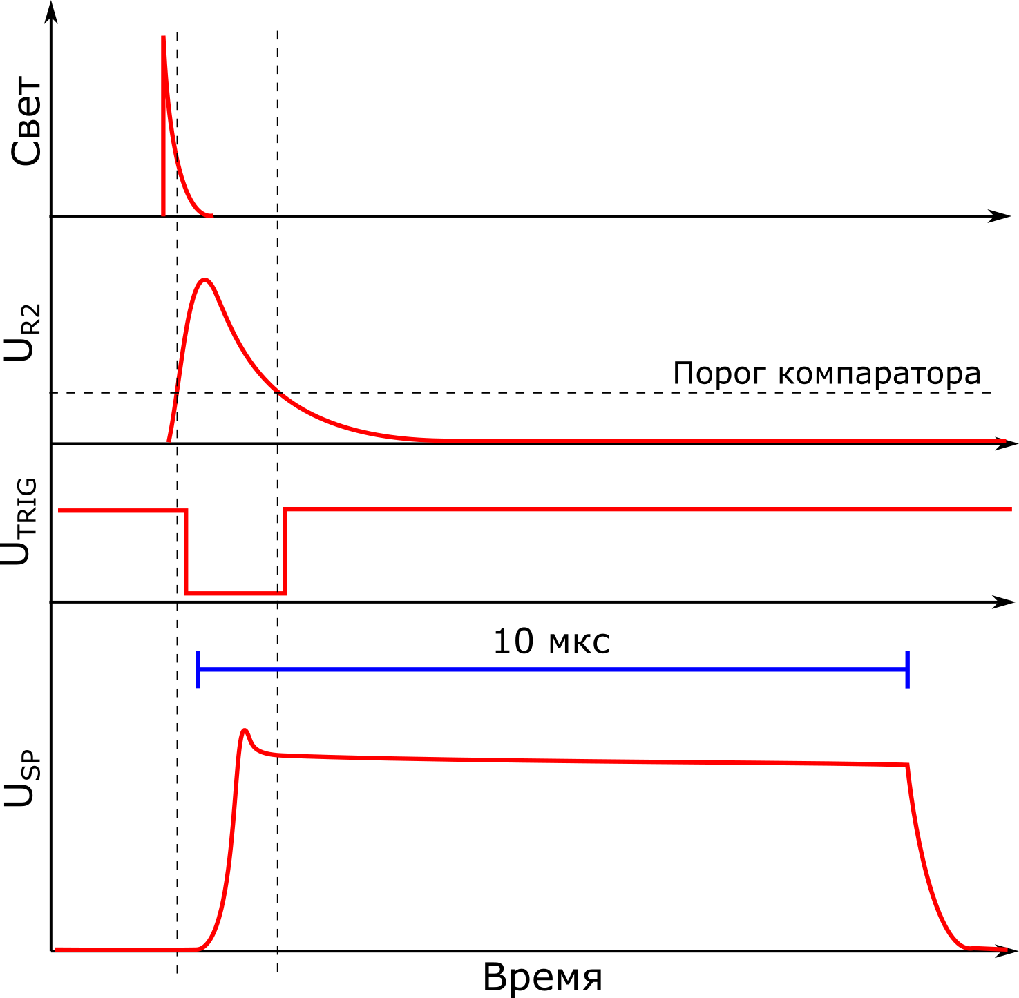
This circuit, when a pulse is received from the detector at the input, generates a zero-level pulse at the TRIG output with a duration of 2-4 μs and a close to rectangular pulse with a duration of 10 μs with a level proportional to the amplitude of the pulse received from the detector at the output SP. For most of these 10 μs, the voltage level remains constant, which allows it to be measured several times using the built-in ADC of the microcontroller, and the TRIG signal must first “wake up” the MC and start the interrupt handler in which this measurement (together with pulse counting) implemented.
For operation, the circuit requires two supply voltages: 3.3 - 5 V for operation of the circuit and "high" voltage of 28-29 V for biasing the detector. The current consumption is about 2.5 mA. According to the “high voltage” circuit, the current consumption depends on the detector load and at background radiation levels is several microamps. It is assembled on a printed circuit board with a size of 64x22 mm using surface mounting.
After assembly, everything should work right away, but when checking, you need to remember that the TRIG output is a very high-speed comparator output and is capable of generating powerful interference. Because of them, when connected (for example, to an oscilloscope) with a long unshielded conductor, everything will be excited. For the same reason, on my developed version of the board, there is a pickup from this signal to the TRIG signal in the form of a high-frequency “ringing”. When assembling the finished device, the board must be connected to the system board with a minimum length bundle in which the TRIG and SP lines are separately shielded, for example, using adhesive nickel cloth grounded to a common wire.
The following main nodes are located on it:
The power scheme (I immediately apologize for not bringing the further schemes to standards and taken directly from Eagle) is shown in the figure below.
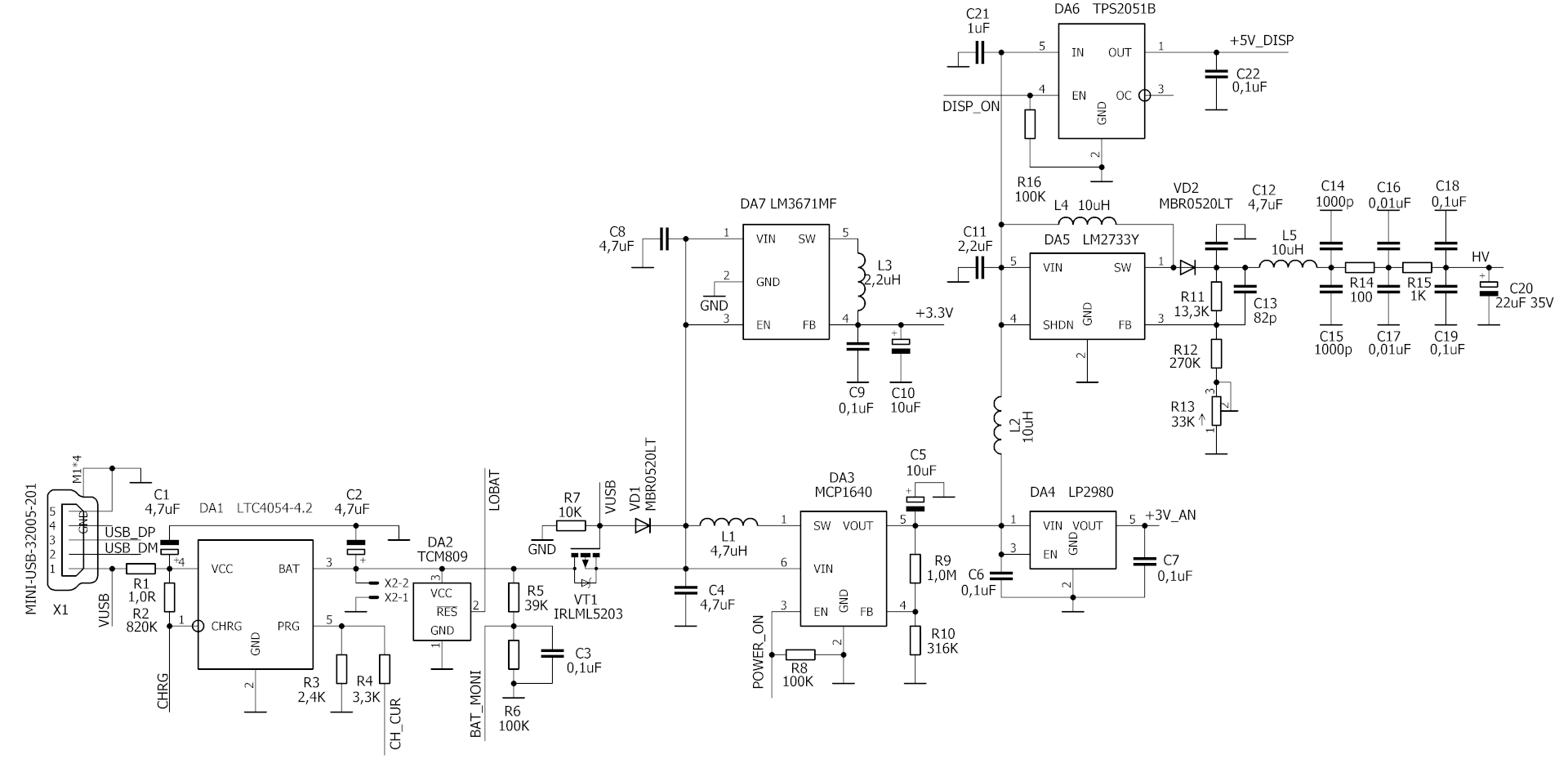
The device is powered by a single-cell lithium-ion battery connected to connector X1. I used a lithium-polymer battery "Robiton" at 2.3 Ah *, in principle, any battery from smartphones, etc. will do. to a similar capacity. On DA1, a charger for it is built, working from a USB port. Here, without any features, all on the datasheet on the LTC4054-4.2. The charging current can be increased from 350 to 700 mA by attracting the lower according to the output circuit of the resistor R4 to the common wire using the MK port. This is then necessary so as not to exceed the allowable 500 mA from the USB port and at the same time allow the battery to charge faster if the device is connected to a network adapter. Using DA2, the MK learns that the battery is dead and turns off the device, and the R5R6C3 divider allows you to measure the voltage on it (wound up on one of the analog inputs of the MK). The CHRG line from DA1 allows the MK to control the state of the charger according to a tricky algorithm: when there is no charge, it has a zero, a unit appears in the charge process that is easily attracted to zero, and when fully charged, it ceases to be attracted and remains one even with a load of several kilograms. In place of DA1, in addition to the expensive original LTC4054-4.2, its clone from ST - STC4054 is also applicable. I caution against using Chinese LTC4054 with Aliexpress: they either do not work at all in any way, or they do not work as they should, killing the battery and creating a threat of its explosion. It was because of this that I refused to use the "popular" TP4056: the original has not been produced for a long time and it is impossible to get it, but the clones either do not have a precharge, then the voltage spread is 4.2 V - almost a volt, then the thermal protection is uprooted ... In general , the only normally working copy of this microcircuit I have is on a small scarf for charging lithium that I once bought. But it’s a pity: she has a simpler indication of the modes, and the maximum charging current is greater, and cooling through the SO-8 with the abdomen is better than through the SOT-23-5 terminals.
The VT1VD1R7 circuit disconnects the load from the battery and switches it to power from the USB port when voltage appears on it, so as not to interfere with the DA1 to properly maintain the charge mode and detect its end.
Next come the converters to get the right supply voltages. The DA3 microcircuit raises the battery voltage to 5 V, the display is powered by them, which increases the converter to obtain 28 V for the detector, and through the linear stabilizer - an analog board. MK can pay off all these consumers by setting zero on the POWER_ON line. The display is blanked separately by the DA6 switch.
To obtain a high voltage, a step-up converter on the DA5 is assembled. The highest voltage version of the LM2731 DC-DC converter has been selected. Initially, it was supposed to use the Chinese MT3608, which is much more economical in this circuit, but it showed very low reliability with an output voltage of 28-29 V (in fact, according to the datasheet, its maximum allowable output voltage is 28 V, so it is not surprising). When setting up this section of the circuit, it should be borne in mind that when the lower arm of the divider (R12R13) breaks, the output voltage jumps to 50-60 V, knocking out the capacitor C20, which is dangerous with an eye injury (they explode very cool!). And if R11 is accidentally shorted, the FB input (pin 3 of DA5) will burn out with the same effect (plus you'll have to change the chip). In this regard, close attention should be paid to the quality of the tuning resistor and the correct installation. An output filter is needed to suppress ripple at the output of this conversion. The converter is closed by a tin screen, soldered around the edges to an earthen landfill on the board.
Instead of DA3, as practice has shown, with the correction of the board, you can install a switch similar to DA6 (accordingly, you do not need a choke and a diode, as well as two resistors R9 and R10). This will make the device somewhat more economical. Then the DA4 stabilizer needs to be installed not at 3.3 V, but at 3.0 so that the analog power supply is stabilized over the entire range of battery discharge.
The DA7 converter works all the time, including when the device is off, providing a 3.3 V MK. At idle, it consumes only a few tens of μA, so that the switched off device almost does not discharge a 2.3 Ah battery. Unfortunately, the STM32L151 does not have a separate input for powering the RTC, which is why I had to make such a decision (or I would have to complicate the switching).
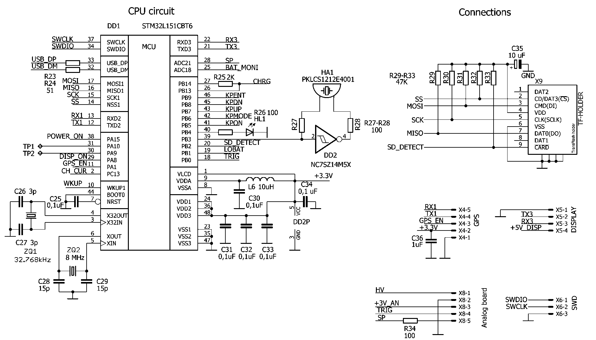

And this is the rest of the system board circuitry.
The heart of the system is MK STM32L151CBT6A (unlike the analogue without index A, it has twice as much RAM - 32 kB). Almost all 48 of his findings were involved. The exceptions were PA9 and PA10, they are also RxD and TxD of the first USART, just in case I made contact pads for them, which are easy to solder in the future. Of the features here is a slightly tricky system for determining the state of the output of the CHRG DA1 with the inclusion of a suspender from PB14, when you need to determine whether the battery is charging or has already been charged, and the tweeter is connected in phase through the DD2 inverter. My error is shown in the diagram: when the MK is switched to STANDBY mode, the input of this inverter is hanging in the air, which leads to significant additional consumption and even generation. Here you need to pull this input to the ground through a 100 kilo resistor. You should pay attention to the quality of quartz resonators, especially ZQ1. With the standard 12 pF clock quartz, the controller’s clock will not work normally, you will have to look for a scarce quartz with a load capacity of 7 pF. To ZQ2 MK is more loyal, but with the first Chinese quartz that came across, here you can catch a lack of start or work on the wrong frequency. Unfortunately, the STM32Lxx line (it is she) is very demanding on the quality of quartz.
The keyboard is connected in a fairly standard way - the port lines are pulled by external resistors R17-R21 to the power and pressed to the ground with buttons. On the keyboard board to suppress chatter, RC chains are soldered in parallel with the buttons. When you press the On button using the DD3 inverter, a high level signal is generated, which is fed to the WKUP input and wakes the MK if it is in the STANDBY state. To prevent accidental switching on from interference, the R22C23 chain is installed. Keyboard lines are connected to consecutive port lines, which allows you to read it in a single port read command.
A microSD card is connected in SPI mode due to the absence of an SDIO controller in this MK. The USB port is connected in the simplest way through two resistors in the DP and DM lines. The STM32 MKs themselves are quite “oak” in terms of statics, and there will be no other external communications (except for the SWD firmware) for the radiometer, so you can not do serious port protection against overvoltages.
The power circuit of MK is taken from a datasheet and does not have any features. When adjusting to the L6 inductor, I sequentially added a 100 ohm resistor, this greatly reduced the voltage fluctuations on the VDDA. The capacitance of C30 can be increased to 1 μF by soldering in parallel to it (on the same sites) another capacitor by 0.01 μF.
When power is applied, the 3.3 V source immediately starts working, generating power for the MK. Other power sources are turned off. After starting the MC and initializing the peripherals, it raises the POWER_ON line (port PA15), starting the 5 V source and supplying power to the analog part and the high voltage source. To turn on the power of the display, you need to raise the DISP_ON line (PA8), similarly, to turn on the satellite navigation module, the GPS_EN line (PA1) is raised, but unlike the display, there is no special power switch for it, the power control input of the receiver itself is used (it should be). The display turns off when the device is operating just by removing power from it.
Counting pulses (TRIG) from the analog block are sent to line PB0, causing interruption on the falling edge. Pulses carrying information about the particle energy (SP) are fed to the 21st channel of the ADC. The duration of the “shelf” of this pulse, during which the level remains unchanged, is almost 10 μs, which allows you to make several ADC conversions after the MC “wakes up” and enters the interrupt. Resistor R34 removes the "ringing".
The motherboard has a size of 64x80 mm and is designed to install most resistors and capacitors of size 0603. Most of the elements are installed on one side, except for three capacitors in the power supply circuit of the MK and two resistors that form the battery voltage divider for measuring it.
The analog board starts working immediately if assembled without errors. In the original version, there were no R8 and C9 elements on the board, without them the circuit worked flawlessly from the generator, but the pulse amplitude at the SP output was random and independent of the pulse amplitude at the input. The introduction of these elements corrected the situation.
If the analog part of the device is excited, there is only one struggle with this - shielding the TRIG line and minimizing the length of the connection cable. The connection to the detector should also be shortest and shielded.
R5 must be selected by the reliable passage of pulses given by the detector with the drug americium-241 in the absence of a comparator reaction to the dark noise of the Si-PMT at the maximum operating temperature.
The analog board must be thoroughly and thoroughly washed away from the slightest trace of flux, especially in the area of the peak detector, and it must be well dried and then warmed up at 150 ° C. Insulation resistance even in gigabytes will sharply worsen its work and make it unstable.
Start building the system board from power sources. First, collect a 3.3 V source and make sure it is working. Then - a 5 V source (not forgetting to connect POWER_ON temporarily with the + 3.3 V bus), and then a high-voltage one. Before turning it on for the first time, set R13 to the upper position in the diagram and do not solder C20 until the voltage is set. Set the voltage to 28 V on the high-voltage source. Ensure that the charger works properly by monitoring the battery voltage during charging. After checking the performance and the correct voltage on all power buses, you can solder the MK and all the details related to it. To check the MK, it is advisable to write and flash some Blink into it. Do not forget to flash and display.
The calibration process will be described in the next issue.
This is only the first part of the article. The second will describe the software part and the calibration procedure. In the meantime, for those who can’t wait - handouts .
Eagle files with circuit diagrams and PCB layouts, as well as the current stable version of MK firmware and display, can be downloaded from Google Drive at this link. Only search mode works in this firmware, and the current model in place of the menu. I am not yet ready to lay out a more functional firmware.
Please note: the positional designations in the analog board circuitry in the figure in the article and in the Eagle project do not coincide, also there are no R8 and C9 elements (according to the diagram from the article) that I installed with a scalpel on the finished board.
The wiring of the boards is designed for their factory manufacturing, for LUT, etc. it will have to be recycled (it hurts a lot of vias). Yes, I have some ready-made boards. If anyone needs it - write in a personal agreement.
What is it and why
The vast majority of pocket-sized dosimeters and radiometers are instruments based on a Geiger counter. This type of detector has its advantages, the main of which are simplicity and low cost, but also a number of disadvantages. First of all, this is a very low efficiency of gamma-ray registration and a complete lack of information about their energy. A Geiger counter captures only one gamma-ray of several hundred, while a low-energy scintillation detector provides almost 100% efficiency. As a result, with a natural background with the same dimensions of the detectors, when the Geiger counter gives only 10-15 pulses per minute, the scintillator gives the same number of pulses, but per second. Thus, in order to get at least some idea of the dose rate, we must spend at least a minute on a set of pulses with a Geiger counter, and with a scintillator we can receive information about the radiation situation every second. So the scintillation detector gives us, first of all, the speed of reaction to weak sources of radioactivity.
In addition, the scintillation detector has the property of proportionality. The higher the particle energy, the greater the amplitude of the pulse at the detector output. What is it for? First, this is how we get information about what is the source of radiation. Each radioactive isotope has its own characteristic energy of gamma radiation (or a set of energies). The gamma spectrometry method is based on this. In this device, the average absorbed energy per quantum will be displayed on the screen (not yet done).
Secondly, if we simply count impulses without taking into account energy, we get an unpleasant thing called “a move with rigidity”. Suppose we calibrated our cesium-137 radiometer. And then they were in a place infected with americium-241. The energy of the cesium-137 quantum is 667 keV, America - 59 keV, that is, more than an order of magnitude less. So, with the same number of particles trapped by the detector (and, therefore, with the same readings from the device), the absorbed dose will be more than an order of magnitude less. That is, the measurements will be erroneous. And in order for the radiometer to measure the dose correctly at different energies (that is, to be a dosimeter ), the energy of each registered quantum must be taken into account.
Portable scintillation radiometers-dosimeters have been on the market for a long time. But for the most part these are very expensive devices for professional use. I know of only one device, oriented to home and amateur use - this is Atom Fast manufactured by KB Radar. The rest - Polimaster devices, a number of foreign companies - are very expensive.
In this device I wanted to get the following:
- Autonomous work without reference to a smartphone or other device with its own display (unlike Atom Fast);
- Try to make power compensation;
- Automatic registration of measurements on removable media, in perspective with cartographic reference;
- Cultural appearance, not particularly giving homemade origin to all sorts of different bloodhounds and watchmen.
As a result, the described device was obtained. It is not finished yet, there is still enough work, especially with software.
Main functions
The radiometer operates in one of two modes: search and measurement. In the search mode, the readings of the device are updated every second, while in addition to the readings in digital form, they are displayed in a graph. In the search mode, no attention is paid to errors; in this mode, the device is primarily an indicator. The screen displays: current dose rate, count rate in pulses per second (CPS), as well as the dose rate averaged over the last minute and the integral dose accumulated after the device was turned on or after a reset. In the measuring mode, on the contrary, the measurement time is set by the operator (by pressing the “Enter” button to start and then to end the measurement), and the calculated error is displayed on the screen along with the measured value, and a mini-journal of the last few is displayed in its “basement” measurements. Moreover, in the measuring mode, the first attempt was made to take into account the energy of quanta and compensate for the “stroke with rigidity”. The measuring mode is in deep under construction and it is not yet in the given firmware version.
Regardless of the mode, the second-second cycle of measurements continues, with the results being saved to RAM. In particular, due to this, when switching to the search mode, the graph displays the readings that were during the stay of the device in the measurement mode, as well as during menu entries, etc. Regardless of the mode, the alarm for exceeding thresholds also works.
There are three thresholds in the latter. The traditional first and second - are set through the menu at the request of the operator and when they are triggered by the results of the next second counting cycle, a sound signal sounds. In addition to them, there is also an adaptive threshold. It is automatically set at an average level per minute, setting at one, two or three sigma (you can select in the settings) from it. If an operation on this threshold occurs in the next cycle, the value from the previous cycle is taken for the next cycle, so that with a slow but steady increase in radiation, a stable alarm is achieved. Subsequently, a log of alarms will be implemented, but so far it is not.
It has not yet been implemented to save the measurement results to a microSD card, the connector for which is mounted on the radiometer board. It also provides for the connection of a GPS module, the use of which is also a matter of the future.
Switching modes and quick change of some settings is done through the "hot keys", the rest of the operations - using the menu. Entering the menu, as already mentioned, does not stop the measurement process.
General plan of the device
The radiometer is mounted in a standard Chip-and-Dip case Gainta G1389G measuring 122x77x25 mm. On the upper panel there is a 3.5 ”color LCD with a resolution of 480x320 pixels. The display uses the Nextion NX4832T035 HMI module, which differs from conventional displays by its own microcontroller, which contains a ready-made program for displaying interface elements, but we just need to send commands to display them, remove or change them - for example, change one or another digit, draw another point on the chart or change the color of one or another inscription. Under the display is a keyboard of five buttons. There is space left for the GNSS receiver, and a scintillation detector is located at the upper end.
Red numbers indicate: 1 - display module, 2 - keyboard, 3 - detector, 4 - analog board, 6 - system board.
The electronic circuit of the device (not counting the display and the navigation receiver, as well as the keyboard) is assembled on two printed circuit boards. On the first, the analog part of the device is assembled, on the second - everything else: a microcontroller with a strapping, a power circuit and its switching, battery charging and a high voltage source for the detector.
Detector
A thallium activated scintillation crystal of cesium iodide is used as a detector in the radiometer. This crystal has the property of radioluminescence - charged particles and high-energy photons (X-ray and gamma range) excite a glow in it, and light is emitted in the form of a short, about a microsecond, flash of light - scintillation. This flash is too weak to be seen with the eye or detected in the usual way. Photocells, photodiodes and photoresistors are too insensitive for this. To assess the scale of the disaster, I will cite the following figures.
A gamma ray with an energy of 1 MeV, completely absorbed in a CsI (Tl) crystal, generates approximately 40,000 photons of green light. Let us try to catch this light with a photodiode. Suppose they all get on a photodiode (in fact, this is unrealistic and good if only half of them get on it). And let's say that we have an ideal photodiode, with a quantum output of 100%. This means that each of the photons will create one electron-hole pair in the structure of the photodiode. And for the momentum we get 40,000 photoelectrons. And this pulse lasts, as we know, 1 μs. So, in a second we will have 4 ∙ 10 10 photoelectrons. The electron charge is 1.6 ∙ 10 -19 C, and the charge 4 ∙ 10 10 photoelectrons is 6.4 ∙ 10 -9Kl, that is, the current strength that the scintillation flash will cause in our photodiode is just a few nanoamps! And if you remember that not all photons also get on the photodiode, and its quantum yield is not 100% ... And besides, the megaelectron-volt is the energy of rather hard gamma radiation, and it would be nice to see much lower energies. In general, photodiodes are practically not suitable for us here. Rather, they are suitable - but with great difficulty.
Usually photoelectronic multipliers were used (and are now used) to capture such weak pulses of light. In them, each photoelectron knocked out of the photocathode multiplies on the dynode system, giving a gain of millions of times, and the current pulse at its anode is no longer nano, but milliamperes, and registering such a pulse is no longer difficult. But PMTs are a solid size fragile glass cylinder, these are kilovolts of power, which in addition require high stability. In general, it is poorly represented in a pocket-sized device.
Fortunately, semiconductor photodetectors are now available that can compete in sensitivity with PMTs. Who said avalanche photodiodes? Yes, it's almost them. Only avalanche diodes, although they have an internal photocurrent gain due to the avalanche multiplication of carriers, have a number of technological problems that do not allow making a sensitive area with a diameter of at least a few millimeters. In addition, the classic avalanche diode has an avalanche amplification coefficient without complex tricks of only 10-200, which is minuscule compared to the million-fold amplification characteristic of a PMT. All these disadvantages of the avalanche photodiode are eliminated in the recently appeared on the market Si-PMT or SiPM. They are essentially a matrix of many avalanche photodiodes operating in pre-breakdown mode, in which a single photon is capable of provoking the development of avalanche breakdown. This mode is similar to the operation of the Geiger counter. Each of the cells has its own blanking scheme, due to which the avalanche breakdown immediately ceases and the cell becomes again ready to register a new photon. All cells (with their quenching schemes) are connected in parallel on a Si-PMT crystal, and the current pulses flowing through them are summed, so that the average current is proportional to the illumination of the crystal. And it is very simple to use such a silicon PMT - it is enough to apply a reverse bias to it - about 28-29 V through a resistor of several kilo-ohms, from which the signal can be taken. Nothing more is needed - neither a kilovolt power source, nor a divider for dynodes. And the Si-PMT itself is a small silicon square measuring 3x3 or 6x6 mm. By the way
So, our detector uses Si-PMTs and a CsI (Tl) crystal, between which a layer of optical lubricant is applied to eliminate the air gap between the crystal and the photodetector window. And on top of the crystal and Si-PMT are covered with many layers of a thin fluoroplastic film, known as FUM tape. This coating has a very high diffuse reflectance. The detector is covered with aluminum tape on top, providing protection from external light and sealing - the cesium iodide crystal is extremely soluble in water and the smallest trace of moisture entering the detector would destroy it. Fortunately, unlike its "relative" - sodium iodide, CsI practically does not have the property of hygroscopicity - that is, it does not attract moisture from the air. Sodium iodide crystals have to be processed only in an absolutely dry inert gas environment and placed in such high-sealed containers as if it would be necessary to create an ultrahigh vacuum in them, and in ordinary air they just blur before our eyes. And vice versa, cesium iodide in the form of single crystals can be easily treated in air (for example, sawed with an ordinary hacksaw for metal and sanded with a sandpaper), avoiding only traces of liquid water and remembering that the crystal contains extremely toxic thallium. However, due to the smallness of its amount, acute (but not chronic!) Toxicity will be determined by iodine, not thallium. Cesium iodide in the form of single crystals can be easily treated in air (for example, sawed with an ordinary hacksaw for metal and sanded with a sandpaper), avoiding only traces of liquid water and remembering that the crystal contains extremely toxic thallium. However, due to the smallness of its amount, acute (but not chronic!) Toxicity will be determined by iodine, not thallium. Cesium iodide in the form of single crystals can be easily treated in air (for example, sawed with an ordinary hacksaw for metal and sanded with a sandpaper), avoiding only traces of liquid water and remembering that the crystal contains extremely toxic thallium. However, due to the smallness of its amount, acute (but not chronic!) Toxicity will be determined by iodine, not thallium.
I will not give advice on the independent manufacture of the detector, since I did not deal with it (the finished detector was kindly provided to me by their developer and manufacturer KBRadarin exchange for some valuable artifacts for electronic engineers), I will give only its parameters. They are: the size of the crystal is 8x8x50 mm, and the Si-PMT MicroFC 30035 of the Irish company SensL (now it is an On Semi division) as a photodetector. A variety of manufacturing tips can be found online. With a slight increase in size, you can take a standard CsI (Tl) or NaI (Tl) crystal in a “native” package of small sizes (10x40, 18x30 mm, etc.). True, the larger the size of the output window, the worse the photodetector with a size of 3x3 mm will work, so I strongly recommend taking a larger (and much more expensive) MicroFC 60035 with the diameter of the output window larger. By the way, the Broadcom analogs of these photodetectors are not recommended to use.
CsI (Tl) crystals were processed as follows. In all samples, the lateral surface was matted. The grinding of the ends was carried out first on thin sandpaper, and then on silk cloth. For better grinding, cerium oxide diluted in ethyl alcohol was used. When grinding glass transparency was achieved. If it was necessary to reduce the crystal to large thicknesses, then it was simply sawn with a thread dipped in water. Then the processing was carried out in the same sequence.
(Gorbunov V.I., Kuleshov V.K. On the question of choosing the optimal size of scintillators for defectoscopy of products // Izv. Tomsk Polytechnic Institute. 1965. V.138. P.42-48.)
Analog part
Its scheme is shown in the figure above. It consists of the following main nodes:
- Input circuit;
- Comparator;
- Peak detector.
The detector is connected to the XP1 input connector. The Si-PMT cathode - to pin 3 (HV), the anode - to pin 1 (DET), and to the pin 2 (GND) the metal screen of the detector is connected - its wrapper is made of aluminum adhesive tape.
The input circuit consists of the load resistance of detector R2 and current-limiting resistance R1, which will try to protect the detector in case of trouble such as accidentally supplying too high a reverse bias voltage or incorrectly supplying a voltage of reverse polarity instead, if the detector itself is connected incorrectly. Together with the capacitance of a silicon PMT (approximately 900 pF), they form voltage pulses with a rise time of about 1 μs and a fall time of about 15 μs. Before applying to the input of the comparator, the signal is passed through a 470 pF capacitor, which decouples the circuit by direct current and, together with the input resistance of the divider R3R5R6, shortens the pulse to 2-3 μs.
An LMV7239 microcircuit was used as a comparator, combining low power consumption with sufficiently high speed (<100 ns) at low differential input voltages. The voltage divider R3R5R6 together with the integrating circuit R4C3 form a “floating” threshold voltage, making the comparator somewhat insensitive to the dark current of the detector and changes in the input current with temperature. The sensitivity of the comparator is controlled by the selection of resistance R5 in the range of several tens of Ohms. A rectangular pulse of negative polarity is formed at the output of the comparator. The trailing edge of this pulse may rattle slightly due to detector noise, but an attempt to get rid of this bounce by introducing hysteresis has led to a decrease in sensitivity and, in general, worse results.
A single-shot on the DA2 integrated timer (LMC555CM, in fact - a conventional 555 timer, only in CMOS version) generates a pulse (positive polarity) of a duration of 10 μs at the leading edge of the pulse at the output of the comparator (specified by the R7C6 timing chain). This pulse is inverted using DD1 (a single TinyLogic inverter in the SOT23-5 package) and applied to the DD2 key, which shorts the peak detector capacitor C12 in the absence of input pulses. At the moment of arrival of the pulse, the short circuit is removed by the indicated 10 μs.
The peak detector is constructed according to the classical non-inverting circuit. The disadvantages of this scheme are well known, but in this embodiment, one interesting thing arises. The fact is that, in anticipation of a pulse, the feedback loop of DA2.1 is broken and the op-amp at the moment of arrival of the input pulse should be in an overload condition, the output of which takes a lot of time, and the state of the amplifier before the pulse is not determined at all (from which all disadvantages of peak detectors of this type). On the other hand, the voltage at the non-inverting input at the preceding moment is close to zero, and the capacitor is shorted, so that the voltage at the inverting input is also zero. At the moment of arrival of the pulse, the output of the op-amp at this moment is in short-circuit mode and the protection circuits from it cover the op-amp with an internal feedback circuit limiting the output current! Because of this, the output stage of the amplifier is no longer in the limiting mode, but it is forcibly entered into the linear mode, from which it already exits easily and quickly. As a result, such a peak detector works much faster than if it was reset at the end of the pulse by short-circuiting the capacitor C12.
A condition for the normal functioning of this circuit is the absence of a constant component in the detector signal, which immediately puts the op-amp in overload mode, and a significant current will flow through the diode and a shorted capacitor (limited, however, by the mentioned built-in feedback circuit, so that nothing will burn out). Therefore, the input and here is the isolation capacitor C9. Resistor R8 provides discharge of this capacitor if it suddenly charges (otherwise it has nowhere to discharge - the input impedance of DA2 is approaching the teraom). In his absence, funny tricks are observed when the circuit works normally for a while, and then suddenly stops, and restores work after a while.
The parameters of the peak detector capacitor usually directly depend on how well it will work. Usually they put a non-polar film, often a fluoroplastic, since low absorption with low leakage is needed. Here, the requirements for it are mitigated by the fact that it is constantly shorted in the absence of a pulse (which suppresses the absorption effect) and by the fact that the charge storage time is only 10 μs, therefore, a high-quality ceramic capacitor of size 1206, necessarily with a dielectric of type NP0, is quite applicable here.
A buffer with a high input resistance is assembled on the second op-amp of DA2 microcircuit, which allows removing voltage from the capacitor of the peak detector without discharging it, the amplification of which is given by resistors R9 and R10.
This circuit, when a pulse is received from the detector at the input, generates a zero-level pulse at the TRIG output with a duration of 2-4 μs and a close to rectangular pulse with a duration of 10 μs with a level proportional to the amplitude of the pulse received from the detector at the output SP. For most of these 10 μs, the voltage level remains constant, which allows it to be measured several times using the built-in ADC of the microcontroller, and the TRIG signal must first “wake up” the MC and start the interrupt handler in which this measurement (together with pulse counting) implemented.
For operation, the circuit requires two supply voltages: 3.3 - 5 V for operation of the circuit and "high" voltage of 28-29 V for biasing the detector. The current consumption is about 2.5 mA. According to the “high voltage” circuit, the current consumption depends on the detector load and at background radiation levels is several microamps. It is assembled on a printed circuit board with a size of 64x22 mm using surface mounting.
After assembly, everything should work right away, but when checking, you need to remember that the TRIG output is a very high-speed comparator output and is capable of generating powerful interference. Because of them, when connected (for example, to an oscilloscope) with a long unshielded conductor, everything will be excited. For the same reason, on my developed version of the board, there is a pickup from this signal to the TRIG signal in the form of a high-frequency “ringing”. When assembling the finished device, the board must be connected to the system board with a minimum length bundle in which the TRIG and SP lines are separately shielded, for example, using adhesive nickel cloth grounded to a common wire.
Motherboard
The following main nodes are located on it:
- Power supplies and their switching circuit, including battery charging circuit;
- The microcontroller and everything you need for its work;
- Auxiliary circuits for keyboard, display, SD card, etc.
The power scheme (I immediately apologize for not bringing the further schemes to standards and taken directly from Eagle) is shown in the figure below.
The device is powered by a single-cell lithium-ion battery connected to connector X1. I used a lithium-polymer battery "Robiton" at 2.3 Ah *, in principle, any battery from smartphones, etc. will do. to a similar capacity. On DA1, a charger for it is built, working from a USB port. Here, without any features, all on the datasheet on the LTC4054-4.2. The charging current can be increased from 350 to 700 mA by attracting the lower according to the output circuit of the resistor R4 to the common wire using the MK port. This is then necessary so as not to exceed the allowable 500 mA from the USB port and at the same time allow the battery to charge faster if the device is connected to a network adapter. Using DA2, the MK learns that the battery is dead and turns off the device, and the R5R6C3 divider allows you to measure the voltage on it (wound up on one of the analog inputs of the MK). The CHRG line from DA1 allows the MK to control the state of the charger according to a tricky algorithm: when there is no charge, it has a zero, a unit appears in the charge process that is easily attracted to zero, and when fully charged, it ceases to be attracted and remains one even with a load of several kilograms. In place of DA1, in addition to the expensive original LTC4054-4.2, its clone from ST - STC4054 is also applicable. I caution against using Chinese LTC4054 with Aliexpress: they either do not work at all in any way, or they do not work as they should, killing the battery and creating a threat of its explosion. It was because of this that I refused to use the "popular" TP4056: the original has not been produced for a long time and it is impossible to get it, but the clones either do not have a precharge, then the voltage spread is 4.2 V - almost a volt, then the thermal protection is uprooted ... In general , the only normally working copy of this microcircuit I have is on a small scarf for charging lithium that I once bought. But it’s a pity: she has a simpler indication of the modes, and the maximum charging current is greater, and cooling through the SO-8 with the abdomen is better than through the SOT-23-5 terminals.
The VT1VD1R7 circuit disconnects the load from the battery and switches it to power from the USB port when voltage appears on it, so as not to interfere with the DA1 to properly maintain the charge mode and detect its end.
Next come the converters to get the right supply voltages. The DA3 microcircuit raises the battery voltage to 5 V, the display is powered by them, which increases the converter to obtain 28 V for the detector, and through the linear stabilizer - an analog board. MK can pay off all these consumers by setting zero on the POWER_ON line. The display is blanked separately by the DA6 switch.
To obtain a high voltage, a step-up converter on the DA5 is assembled. The highest voltage version of the LM2731 DC-DC converter has been selected. Initially, it was supposed to use the Chinese MT3608, which is much more economical in this circuit, but it showed very low reliability with an output voltage of 28-29 V (in fact, according to the datasheet, its maximum allowable output voltage is 28 V, so it is not surprising). When setting up this section of the circuit, it should be borne in mind that when the lower arm of the divider (R12R13) breaks, the output voltage jumps to 50-60 V, knocking out the capacitor C20, which is dangerous with an eye injury (they explode very cool!). And if R11 is accidentally shorted, the FB input (pin 3 of DA5) will burn out with the same effect (plus you'll have to change the chip). In this regard, close attention should be paid to the quality of the tuning resistor and the correct installation. An output filter is needed to suppress ripple at the output of this conversion. The converter is closed by a tin screen, soldered around the edges to an earthen landfill on the board.
Instead of DA3, as practice has shown, with the correction of the board, you can install a switch similar to DA6 (accordingly, you do not need a choke and a diode, as well as two resistors R9 and R10). This will make the device somewhat more economical. Then the DA4 stabilizer needs to be installed not at 3.3 V, but at 3.0 so that the analog power supply is stabilized over the entire range of battery discharge.
The DA7 converter works all the time, including when the device is off, providing a 3.3 V MK. At idle, it consumes only a few tens of μA, so that the switched off device almost does not discharge a 2.3 Ah battery. Unfortunately, the STM32L151 does not have a separate input for powering the RTC, which is why I had to make such a decision (or I would have to complicate the switching).
And this is the rest of the system board circuitry.
The heart of the system is MK STM32L151CBT6A (unlike the analogue without index A, it has twice as much RAM - 32 kB). Almost all 48 of his findings were involved. The exceptions were PA9 and PA10, they are also RxD and TxD of the first USART, just in case I made contact pads for them, which are easy to solder in the future. Of the features here is a slightly tricky system for determining the state of the output of the CHRG DA1 with the inclusion of a suspender from PB14, when you need to determine whether the battery is charging or has already been charged, and the tweeter is connected in phase through the DD2 inverter. My error is shown in the diagram: when the MK is switched to STANDBY mode, the input of this inverter is hanging in the air, which leads to significant additional consumption and even generation. Here you need to pull this input to the ground through a 100 kilo resistor. You should pay attention to the quality of quartz resonators, especially ZQ1. With the standard 12 pF clock quartz, the controller’s clock will not work normally, you will have to look for a scarce quartz with a load capacity of 7 pF. To ZQ2 MK is more loyal, but with the first Chinese quartz that came across, here you can catch a lack of start or work on the wrong frequency. Unfortunately, the STM32Lxx line (it is she) is very demanding on the quality of quartz.
The keyboard is connected in a fairly standard way - the port lines are pulled by external resistors R17-R21 to the power and pressed to the ground with buttons. On the keyboard board to suppress chatter, RC chains are soldered in parallel with the buttons. When you press the On button using the DD3 inverter, a high level signal is generated, which is fed to the WKUP input and wakes the MK if it is in the STANDBY state. To prevent accidental switching on from interference, the R22C23 chain is installed. Keyboard lines are connected to consecutive port lines, which allows you to read it in a single port read command.
A microSD card is connected in SPI mode due to the absence of an SDIO controller in this MK. The USB port is connected in the simplest way through two resistors in the DP and DM lines. The STM32 MKs themselves are quite “oak” in terms of statics, and there will be no other external communications (except for the SWD firmware) for the radiometer, so you can not do serious port protection against overvoltages.
The power circuit of MK is taken from a datasheet and does not have any features. When adjusting to the L6 inductor, I sequentially added a 100 ohm resistor, this greatly reduced the voltage fluctuations on the VDDA. The capacitance of C30 can be increased to 1 μF by soldering in parallel to it (on the same sites) another capacitor by 0.01 μF.
When power is applied, the 3.3 V source immediately starts working, generating power for the MK. Other power sources are turned off. After starting the MC and initializing the peripherals, it raises the POWER_ON line (port PA15), starting the 5 V source and supplying power to the analog part and the high voltage source. To turn on the power of the display, you need to raise the DISP_ON line (PA8), similarly, to turn on the satellite navigation module, the GPS_EN line (PA1) is raised, but unlike the display, there is no special power switch for it, the power control input of the receiver itself is used (it should be). The display turns off when the device is operating just by removing power from it.
Counting pulses (TRIG) from the analog block are sent to line PB0, causing interruption on the falling edge. Pulses carrying information about the particle energy (SP) are fed to the 21st channel of the ADC. The duration of the “shelf” of this pulse, during which the level remains unchanged, is almost 10 μs, which allows you to make several ADC conversions after the MC “wakes up” and enters the interrupt. Resistor R34 removes the "ringing".
The motherboard has a size of 64x80 mm and is designed to install most resistors and capacitors of size 0603. Most of the elements are installed on one side, except for three capacitors in the power supply circuit of the MK and two resistors that form the battery voltage divider for measuring it.
Assembly and commissioning tips
The analog board starts working immediately if assembled without errors. In the original version, there were no R8 and C9 elements on the board, without them the circuit worked flawlessly from the generator, but the pulse amplitude at the SP output was random and independent of the pulse amplitude at the input. The introduction of these elements corrected the situation.
If the analog part of the device is excited, there is only one struggle with this - shielding the TRIG line and minimizing the length of the connection cable. The connection to the detector should also be shortest and shielded.
R5 must be selected by the reliable passage of pulses given by the detector with the drug americium-241 in the absence of a comparator reaction to the dark noise of the Si-PMT at the maximum operating temperature.
The analog board must be thoroughly and thoroughly washed away from the slightest trace of flux, especially in the area of the peak detector, and it must be well dried and then warmed up at 150 ° C. Insulation resistance even in gigabytes will sharply worsen its work and make it unstable.
Start building the system board from power sources. First, collect a 3.3 V source and make sure it is working. Then - a 5 V source (not forgetting to connect POWER_ON temporarily with the + 3.3 V bus), and then a high-voltage one. Before turning it on for the first time, set R13 to the upper position in the diagram and do not solder C20 until the voltage is set. Set the voltage to 28 V on the high-voltage source. Ensure that the charger works properly by monitoring the battery voltage during charging. After checking the performance and the correct voltage on all power buses, you can solder the MK and all the details related to it. To check the MK, it is advisable to write and flash some Blink into it. Do not forget to flash and display.
The calibration process will be described in the next issue.
* * *
This is only the first part of the article. The second will describe the software part and the calibration procedure. In the meantime, for those who can’t wait - handouts .
Eagle files with circuit diagrams and PCB layouts, as well as the current stable version of MK firmware and display, can be downloaded from Google Drive at this link. Only search mode works in this firmware, and the current model in place of the menu. I am not yet ready to lay out a more functional firmware.
Please note: the positional designations in the analog board circuitry in the figure in the article and in the Eagle project do not coincide, also there are no R8 and C9 elements (according to the diagram from the article) that I installed with a scalpel on the finished board.
The wiring of the boards is designed for their factory manufacturing, for LUT, etc. it will have to be recycled (it hurts a lot of vias). Yes, I have some ready-made boards. If anyone needs it - write in a personal agreement.