Microelectronics technologies on the fingers: Moore’s Law, marketing moves and why nanometers are not the same now. Part 3
- Transfer
In the third part, the author of the original article discusses Zelenograd, the memory and the meaning of miniaturization on the fingers.
Disclaimer: Once upon a time I dabbled in writing articles about chip manufacturing , and in the series of articles “Inside Look” I even looked inside of them, i.e. The topic is extremely interesting to me. Naturally, I would like the author of the original article to publish it on Habré, but in connection with employment, he allowed me to transfer it here. Unfortunately, the Habr rules do not allow direct copy-paste, so I added links to sources, pictures and a little gag and tried to straighten the text a little bit. Yes, and articles ( 1 and 2 ) on this topic from amartology I know and respect.
Summary of previous episodes
So, what did we learn from the first and second parts?
Until the early 2000s, the main priority in the production of microcircuits for computers was to reduce the size of elements (transistors). Miniaturization made it possible to accommodate more transistors per chip, which reduced the average cost of a single transistor in a microcircuit and allowed increasing clock frequencies, as well as integrating more functionality into one chip. The latter reduced the need for outward access to a slow external bus. The size of transistors almost linearly correlated with the so-called technological process norm: with a decrease in technology by 2 times, the linear dimensions of transistors also decreased by 2 times, and the area - by 4 times. The physical structure of the transistors themselves did not change, the sizes were simply reduced.
Since the beginning of the 2000s, physical limitations began to affect. The sizes of transistors no longer linearly depend on technology. And the less nanometers were declared in the technological process, the weaker this affected the real sizes of the elements. Each step in reducing the size of the technology is now accompanied by a change in the physics of the process. In addition, as miniaturization began, side effects began to appear in the form of an increase in leakage currents and an increase in spurious energy consumption. This put an end to the further increase in processor clock speeds. During the 2000s, a quiet glanders, a change of priorities occurred. Now the main task of the designers was not to reduce the size of transistors, but to reduce leakage currents. The result of this policy was the transition from flat transistors to bulk.
One of the manifestations of the complexity of technological processes has been the increase in the cost of the crystal with each reduction in technology. The cost of manufacturing chips varies according to the same schedule - immediately after the release of a new process technology, the price is maximum due to the low yield of suitable microcircuits, design and optimization costs. As production is being debugged, the cost price decreases, the yield of suitable chips increases. The minimum price at the end of the cycle is before discontinuation. Previously, the cost of a microcircuit, for example, according to the technological process of 3 microns and 1.5 microns, was the same at the same stage of the life cycle. And since the number of transistors in the same area grew 4 times, the price of one transistor decreased 4 times.
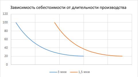
After going below 130 nm, the cost of chips began to grow due to the complexity of technological processes. However, due to an increase in the density of transistors, the cost per one transistor continued to decrease. So it lasted to the 28/32 nm technology. Further, each step was given everything with a high cost of the chip, and the real size of the transistors was reduced less and less. As a result, one transistor on a microcircuit with a norm of 22 nm or lower costs more than a norm of 28 nm ( sailed! ).
About Zelenograd
Most of all, people are interested, of course, in the situation with Russian microelectronics. Unfortunately, not strong in Zelenograd affairs. All I know is that in 2014 Mikron purchased a 90 nm technological line from the French STMicroelectronics just before the crisis. And then on its own it was upgraded to the standards of 65 nm process technology. I guess the French didn’t really like it. The transition to 65 nm was reported at the end of 2014. Periodically produced experimental batches on it. I don’t know whether they went into the series ( Note: it seems to be yes - for memory ). Nevertheless, there are half sovereign 65 nm in Russia.
Note: about Mikron , BarsMonster gave an excellent text , a little more here , a couple more articles ( 1 and2 ) on the topic from amartology .
The main problem is that 65 nm were not very popular. For the main production of Micron, 90 nm and 180 nm are enough, and even - oh, horror! - completely sovereign 250 nm. Some defense microcircuits are still produced using technologies of 3-5 microns ( Note: especially for space, where reliability is important, not speed). Simply, the larger the transistors, the higher the immunity to interference and radiation ( UPD: article on the radiation resistance of circuits with a different opinion). And ultra-large computing power for specialized chips, as a rule, is not needed.
On the other hand, it is more profitable to order the production of modern processors in Taiwan and China according to 28 nm or lower techno- metries ( note: and again we say hello to Baikal ). In this case, the development of architecture and topology is completely Russian, but the manufacturing of crystals takes place in Taiwanese factories. Many are embarrassed that they say that these are not quite our processors. As a reassurance, we can say that almost all world leaders are in the same situation. Own semiconductor production remained only with Intel. Brands such as AMD, Apple, NVidia, Qualcomm, IBM and others are manufactured at TSMC or Samsung factories. So, AMD in 2009 brought its production to a separate company GlobalFoundries, which was bought by the Arabs. They have not mastered the latest technorefused to participate in the development of the 7 nm process technology, concentrated on "more mature" manufacturing processes. Now they are in a pre-bankrupt state, which is scheduled for about 2024 , and engineers are ready to take IBM to themselves .
At the end of 2018, in Mikron, they confirmed their plans to create their own 28 nm production in Zelenograd. They plan to deploy production already in 2022 in a new factory built from scratch. The reality of the deadlines is in great doubt, although, of course, it would be nice. 28 nm is already a different level of production and design, allowing you to start production of fundamentally new products. But more about that below.
In general, the situation in Russian microelectronics is not as rotten as it might seem. Given that 12 years ago, the “thinnest” manufacturing process in the country was 800 nm, even the current all-Russian 250 nm does not look so bad. There are rumors that they mastered the technology of “stretched silicon”, switched from 150 mm plates to 200 mm, and set up the production of their own photo masks. The main problem will remain insufficient demand and competition with imports, which in no way makes it possible to achieve at least zero profitability.
Attempts are underway to master something breakthrough. For example, photolithography in deep ultraviolet (EUV lithography).
In this sense, the story with the Dutch company “Mapper Lithography” is interesting ( BarsMonster wrote about it , as well as an article fromCornelius agrippa ). The company specialized in equipment and systems for multipath electron lithography (MEL).
Electronic lithography allows you to work with resolutions in fractions of a nm, but it is very energy-intensive and slow. Using it make photo masks for optical lithography. Usually one electron beam is used, which irradiates the entire area. The use of MEL would significantly accelerate the process, although the power consumption of the installation has increased significantly.
The Dutch tried to bring MEL into mass production. At least for small-scale microcircuits, where the creation of a set of photo masks does not pay off. Those. where it is cheaper to apply the pattern directly to silicon than to make a set of masks, and then stamp microcircuits using optical lithography. And here Mapper found like-minded persons in the person of RosNano. In 2012, they concluded a contract for the construction of factories in Moscow and St. Petersburg. The factory in Moscow was opened in 2014 and in the same year began production of electronic lenses.
There is no question of profitability yet, but the technologies themselves are and are developing. Taking into account the rise in price of photolithography processes, MEL can become equal in time to it in cost. Unfortunately, RosNano’s investments did not save Mapper Lithography itself. The company was bought by the Dutch ASML- the world's largest manufacturer of photomasks and photolithography systems. The MEL branch was closed, Mapper employees were shoved in other directions ( note: since there are such attendants in the EUV that Goliath cannot stand two). Now in the world there are only 2 players who continue to develop MEL - American Multibeam and RusNano.
Where are small nanometers needed?
Consider the largest contract manufacturer of microelectronics - Taiwanese TSMC. Here is the report for the 2nd quarter of 2018:
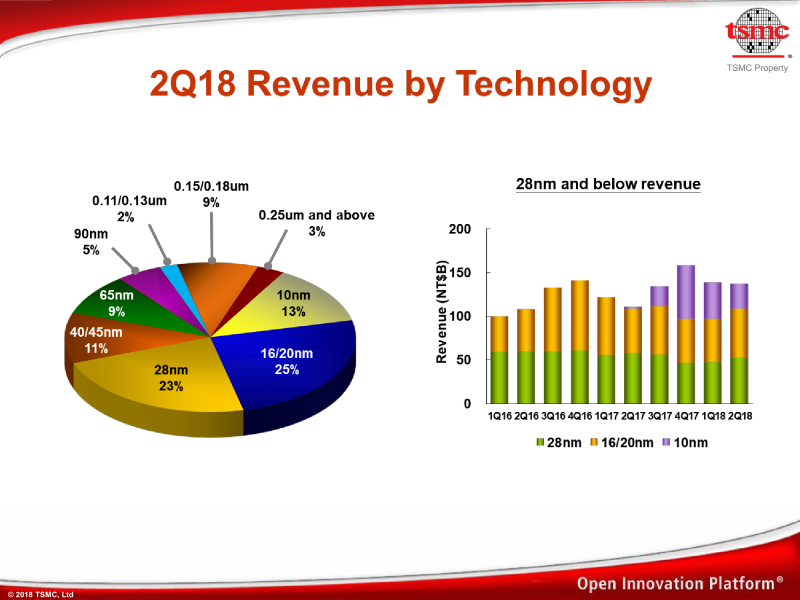
As you can see, the most delicate processes account for only 38% of the company's revenue, and 19% account for 90 nm or more. The German X-FAB , for example, generally uses technologies of only 130 nm and higher, and does not suffer from this.
Consider the main areas of modern electronics:
- Power Electronics Here, subtle processes are not only unnecessary, but even impossible. Since they work only at voltages in the region of 1 V. For power electronics, other impurity concentrations and vertical layer sizes are required. The very concept of a process norm has a different meaning. It is calculated, not based on the smallest technologically possible, but arises from operating voltages and current density. The dimensions of the power elements are calculated based on the peak current strength.
Note: Being at the ABB factory in the glorious city of Lenzburg, I was pleasantly amazed at how wide the range of products they produce and how they make failure analysis of broken current converters. - Industrial electronics. These are various industrial microcontrollers and mechanical control systems. As a rule, they work with voltages ranging from several volts to tens of volts. Working technologies there are usually from 130 nm. Industrial electronics do not require billions of transistors and hundreds of MB cache, as usually a limited set of operations is performed. Microcontrollers are more specialized than microprocessors for computing systems. Part of the code and instructions there are “wired” into the crystal itself at the manufacturing stage, and are not loaded programmatically. Thanks to this, they work faster in native operations. The most important thing here is reliability.
- Military, space and radiation-resistant electronics. Here, the technology starts from 250 nm. Less is simply impossible, because with a decrease in the size of transistors, the number of failures from the effects of radiation and interference increases sharply. As well as industrial electronics, these are usually specialized microcircuits with lower performance requirements.
- Consumer and automobile electronics.Analog, analog-to-digital circuits and digital-to-analog microcircuits. The trend here is the combination of all the functionality (both digital and analog) into one crystal. In addition to power transistors naturally. For example, single-chip TVs. The problem here is that, as a rule, the number of transistors required is small. For the normal functioning of the device, tens of thousands of transistors are enough for the eyes. With technologies smaller than a micron, the entire area they occupy is a fraction of a square millimeter. Often contact pads for conclusions occupy more area than the logic itself. Therefore, they are trying to shove everything that is possible into such microcircuits - an electronic clock with an alarm clock, a radio receiver and other side functions into the chip of the washing machine. The cost is almost the same. There is no point in bothering with small nanometers in such a situation. Moreover, there are limitations due to the presence of analog bipolar transistors and noticeable operating currents. It makes no sense to use less than 90 nm even in the digital part (UPD: amartology 28 nm based CMOS for ADC and DAC ). The situation may change with the spread of the Internet of Things (IoT).
- RFID tags. These are chips for different cards, electronic keys, product tags. They consist of a small microcircuit and a film antenna. The microcircuit is made of reprogrammable memory based on CMOS and induced power control on bipolar transistors. The size of the crystal is less than 1 mm 2 . The number of transistors is usually small, there is no constant power. Therefore, the requirements for the cheapness of one transistor and power consumption are not relevant. The main thing is the duration of storage of the memory value in passive mode. As I already wrote, at rates below 130 nm, leakage currents increase, and, accordingly, in cells the value can be lost. Technological processes below 90 nm are not just not relevant, they are harmful.
Note: RFID parsing is here , and soon there will be a bit more hickporn. - Computer Engineering. Processors, memory, controllers. By value, this is the lion's share of the modern electronics market. Here is the rule: the more transistors in the chip, the better. Unlike specialized controllers, the entire set of commands and instructions is loaded programmatically. Hence the high performance requirements - the price of versatility.
Russian enterprises are able to ( note: with reservations and exaggerations) produce the first 5 groups of microcircuits, except for IoT. True, in terms of market turnover in money, they are collectively much inferior to the 6th group.
The meaning of miniaturization
Some were interested: why is it so important to push the maximum of transistors per unit area? What makes it difficult to just make a larger crystal or make 2 crystals instead of one.
For computer technology this is very important. At modern frequencies, there is a physical limitation on the size of the crystal. This is the speed of light, it is the speed of propagation of an electrical signal. The speed is only 300 million meters per second ( note:this is for vacuum, and it is slightly smaller by the dielectric constant, due to propagation in the medium). In a processor with a clock frequency of 3 GHz, an electrical signal runs 10 cm per cycle. Moreover, not only transistors must change their state per cycle, but all transients must also be able to withstand. To do this, you need a stock of at least 3 times. Those. the farthest transistor in the crystal should not be further than 3 cm from the clock generator. The generator is placed in the center of the chip, which means that the entire circuit should fit into a circle with a radius of 3 cm from the center of the chip (you can check on your PC;)). For a square-shaped crystal, we get a maximum size of 4x4 cm. The higher the frequency, the smaller the limiting sizes.
Heat sink The larger the crystal, the more difficult it is to remove heat from the center. And this is fraught.
The smaller the linear dimensions of the transistors, the smaller the stray capacitance and the faster transients. Accordingly, higher speed and lower recharge current.
Now why is one processor with 4 million transistors, for example, better than 4 processors with 1 million transistors each. For starters, the question of price. A crystal with 4 million transistors will cost slightly more than a crystal with 1 million transistors. Since they are created in a single technical process. In addition to the chip, the microcircuit also consists of a case and gold pins from a crystal. And gold is not cheap metal. Conventionally, for a 1-millionth microcircuit, 300 contacts are needed (1200 for 4-microcircuits), for a 4-millionth one - 308. The benefit is obvious.
Then 4 microcircuits will interact with each other through an external bus, and it is several times slower than the clock frequency of the processor itself (see the paragraph on the speed of light). Note: yes there is a solution from AMD with Infinity Fabric , but this is a separate issue. It turns out that 4 processors can only work in isolated tasks mode. While 4 cores inside a single chip can work as a cluster, quickly distributing tasks and exchanging at the processor clock speed.
Therefore, the desire to make transistors as small as possible, and to cram into the crystal everything that can be rationally justified.
Prospects
It turns out that with the first five groups of microelectronics in Russia, everything is not so bad. Problems with profitability and price, but technological opportunities exist. Computing is harder. You can of course make Baikal or Elbrus using 65 nm technology. This is the era of Intel Pentium 4 ( pichal! ). But only with such scanty series the cost will be prohibitive. Or, as an option, sell below cost at the expense of the budget. And the fig? Until they covered up the opportunity, it is easier and cheaper to produce in Taiwan (which, in fact, is being done).
With access to the world level and large series, it seems hopeless darkness. But here a ray of light appeared. It is associated with the advent of new types of electronic memory. To explain why optimism is connected, you will have to get into the technical details slightly.
The main types of electronic memory
Static RAM or SRAM .
In fact, this is a transistor circuit for
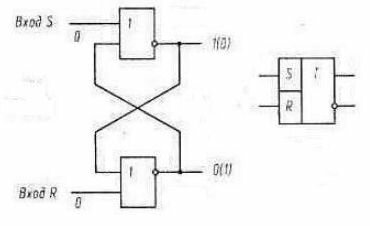
A six-transistor memory cell is standard. Although there are 8- and 10-transistor.
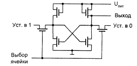
Thanks to the cross feedback inside, it stores its state even in the absence of a signal at the input. While there is food of course. The same MOS transistors are used, they consume only the switching current when the values change. In a static state, only the stray leakage current is consumed.
Pros - high read and write speed (at the clock frequency level), low power consumption, clarity of value storage, standard technology
Cons - volatility, large footprint on the chip.
Usually used as a built-in processor cache. Separate SRAM chips are also produced, but now it is more exotic.
Dynamic random access memory or DRAM .
The dynamic memory cell is one slightly modified CMOS transistor:

The difference from the standard MOS transistor is that the contact to the drain is not connected to the bus, but is transformed into a small flat thin-film capacitor Metal - Dielectric - Silicon. If the capacitor is charged - logical "1", not charged - logical "0". All cell management is carried out by the control circuit - the controller. The memory cells are combined into rows and columns, form a flat matrix. Rows are combined by gates, columns by sources.
When recording, a voltage is applied to the shutter, the transistor opens. If voltage is supplied to the source from the controller at this moment, current appears and the capacitor charges. No voltage, not charging. Recording goes on the whole line at the same time.
Reading is similar, only the controller is in read mode. The voltage is applied to the gates. If the capacitor was charged, current will flow (logical 1), if not charged, there is no current (logical 0). The entire line is also read at once. After reading the capacitors are discharged, all cells are set to 0. Based on the data received, the controller re-writes the line.
In fact, reading and writing occur constantly, even in the absence of activity. The fact is that the capacitance of the capacitor is very small, it quickly discharges, within milliseconds or tens of ms. Therefore, the background is continuous regeneration (reading and re-writing lines). As soon as the regeneration stops, within hundredths of a second, the data in all cells is reset.
The advantages of dynamic memory are compactness.
Cons - lower speed, high power consumption, control complexity, energy dependence.
However, despite all the shortcomings, all RAM modules are now type DRAM. Except rare exotic. Compactness overpowered everything.
Reprogrammable memory, Flash memory and EEPROM .
It is based on field-effect transistors with a floating gate:

Under the control gate there is another, not connected to anything and surrounded by a dielectric on all sides - “floating gate”. The charge enters the floating gate and affects the formation of the channel. There is nowhere to charge from the floating shutter, so the cell retains its value even when the power is off. Depending on the degradation of the surrounding dielectric, the charge can be stored from several months to tens of years.

In the simplest case, to obtain a unit, you can drive a positive charge, then the transistor will be open all the time. In real life, a negative charge is used, which even more “locks” the channel.
How is reading. A positive voltage is applied to the control gate just above the threshold. If the floating gate is discharged, a channel is formed in the base and the transistor opens - logical “1”. If charged, it compensates for the voltage of the control gate, and the channel is not formed. The transistor is closed, a logical "0".
Reading is simple. The main problem is recording. It is necessary to drive the charge into an insulated shutter or remove it. At different times, they used ultraviolet irradiation, avalanche breakdown, injection of high-energy electrons, and tunnel breakdown.
With an avalanche breakdown it is clear. They give a high voltage, it breaks through the dielectric and charges the floating gate. To discharge breakdown in the other direction. But avalanche breakdown is such a thing, it is like an electric shock for a person. Killing will not kill, but after the 10th time, health can be shaken. Therefore, the number of rewrite cycles was limited.
During injection of electrons, breakdown does not occur, simply under the influence of voltage, electrons with a high level of energy break through the oxide and fall into the floating gate (or from it). The disadvantages of the method are the duration of the dubbing and high voltage.
With thinning of the dielectric layers to unity nm, it became possible to charge and discharge a floating gate using the tunnel effect. By the electric field we shift the energy structure of the words so that opposite the shutter there are either levels filled with electrons or free levels. Then the electrons tunnel either there or back. Thanks to this, the number of rewriting cycles has reached thousands or tens of thousands. Depends on the material and the quality of the dielectric.
Advantages - energy independence, compactness, decent reading speed.
Cons - long recording time, high recording voltage, degradation as you work.
Used in SSD devices and RFID tags.
Note: by the way, the flash drive was also sawed at the time for experiments ...
Magnetoresistive memory, MRAM .
A new type of memory. The principle of operation is similar to DRAM, but instead of an electric capacitor, a magnetoresistive cell is used. A magnetoresistive cell is a structure whose electrical resistance depends on the direction of the magnetic domains.
It consists of 2 layers of a ferromagnet, between which a thin (about 1 nm) dielectric film. The first layer is a ferromagnet with constant magnetization, the second with a variable, the so-called free layer. If the domains of the first and second layer are located in the same direction, the electrons can actively tunnel through the dielectric, high tunneling current. If the domains are oppositely oriented, then the tunneling current is orders of magnitude weaker.
Schematically, a magnetoresistive cell can be represented as a resistor with two resistance values - high and low. The free layer stores the magnetization vector indefinitely and without external power. That is, this type of memory energy does not depend on.
With reading, everything is simple: we apply voltage to the gate of the transistor, and a magnetoresist begins to flow through it. If the resistance of the manitoresist is high, then a weak current, if low, then a strong current. By the magnitude of the current, a logical “0” or “1” is determined.

Problems with the recording again. Dozens of methods are being developed, each of which has its own abbreviation.
Initially, the rewriting of the free layer was carried out by a strong current. But this is a high power consumption when recording. Plus, in this case, the cell cannot be made smaller than hundreds of nm, otherwise neighboring cells will also be recharged. This type of memory chip has a maximum capacity of 16 MB.
Therefore, other methods are being developed - by local thermal heating, stepwise, using antiferromagnets, by spin current. The latter option now seems to be the most promising. The physics there is complex, turning into quantum mechanics. Therefore, let’s forget for clarity.
Another advantage of MRAM is that magnetoresistive cells do not require alienation of space on the chip. They are located above, above the CMOS structure. Those. first we form all the CMOS layers, the first metallization layers, everything is covered with oxide. Then on top of the solid first layer of a ferromagnet. We corrode the excess, then the same with the dielectric layer and the second ferromagnet. It turns out a very compact structure.
Magnetoresistive memory is now considered the most promising. Some even claim that with its introduction into the series, the separation of memory into operational and permanent will disappear altogether. It will be just a memory. In particular, the OS will not need to be loaded, it will immediately work from memory when the power is turned on. Like TR-DOS on Sinclair in the good old days. There, the OS kernel worked from ROM.
What place does Russia occupy here. In the development of MRAM, our, although not leaders, are on the front line. Anyway, bye. There is such a Russian company, Crocus Nanoelectronics , which deals with STT MRAM memory, i.e. MRAM spin transfer ( more ).
This gives our manufacturers a window of opportunity to break into the global market for computer chip manufacturers. The window is not very large, but it is. Need free will, money, and our own 28nm process technology.
Conclusion
I believe that one of our main problems is the mentality. This is a habit of falling into emotions, giving up and self-flagellation. Instead of working methodically and purposefully. In microelectronics, this is especially acute. You just need to remember the old Russian proverb: eyes are afraid, and hands are doing.
World leaders rested in physical limitations, the industry is moving from rapid growth to slow development. Breakthroughs such as quantum processors are still on the far horizon. Closer than teleportation, but most likely not in our lives. In the next 20 years, among the players on the field of microelectronics, the composition of the leaders can radically change. The main thing here is not to click the beak.
Part 1 and part 2 .
Do not forget to subscribe to the blog : it’s not difficult for you - I am pleased!
And yes, please write about the shortcomings noted in the text in the PM.
PS: A minute of advertising. In connection with the latest trends of “fashion”, I would like to mention that this year Moscow State University opens a permanent campus (and has been teaching for 2 years!) Of a joint university with the Beijing Polytechnic in Shenzhen. There is an opportunity to learn Chinese, as well as get 2 diplomas at once (IT specialties from VMK MSU available). More information about the university, directions and opportunities for students can be found here . Reception of documents - until July 10!
A short video for clarity about the ongoing lawlessness