"Cell" breadboard
- Transfer
Once again thinking about prototyping electronics, the author also wondered: which layout of the breadboard would be optimal (in the sense of being the most flexible) for working with small SMD components, in particular in cases like SOT23-3.
There are many options, but basically they "grow legs" from the original Veroboard topology - a board with two-dimensional mass of holes in 0.1-inch increments, with horizontal conductors that can be cut where necessary. There are also options with pads that are not connected to each other, connected in pairs, and even without printed conductors at all.
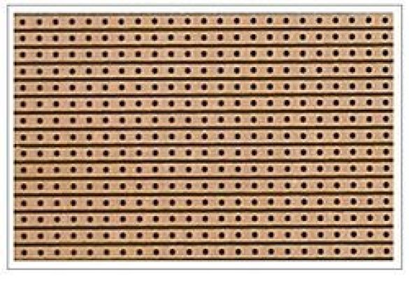
Veroboard Board Source: Wikipedia
The rights to the name Veroboard many times passed from one company to another, until they returned to the English company Vero Technologies, next to which the author lives. Somehow he might even glance there. The names perfboard, stripboard are also known.
Next, there are breadboard boards that do not require soldering, which allows you to repeatedly remake the circuit and change components without damaging them. But such boards, unlike the previous ones, are unsuitable for working with SMD components if you do not solder the legs to them. Such boards include, for example, Adafruit Perma-Proto.
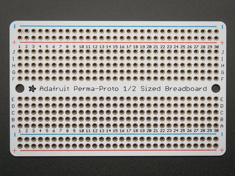
Adafruit Perma-Proto Board Source: Adafruit Website
The next option is to place as many different types of contact pads on one universal board as possible so that they come to the maximum possible number of types of components. As, for example, made in the Universal Prototyping Board from Mike's Electric Stuff.
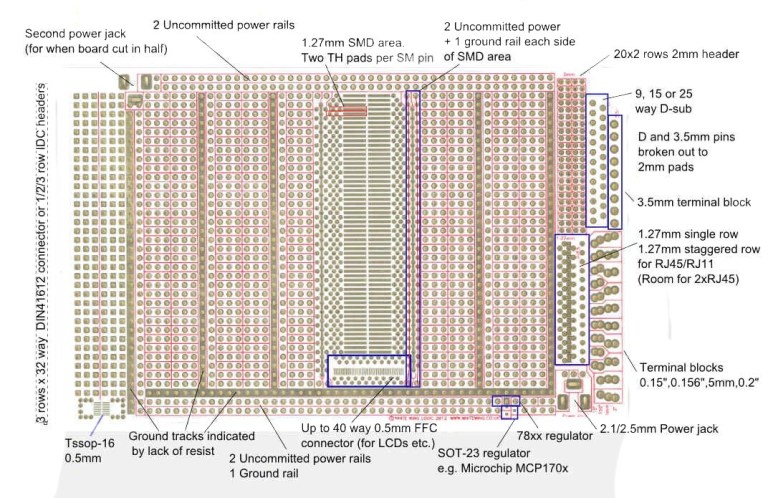
Universal Prototyping Board by White Wing Design. Source: whitewing.co.uk
This, of course, with a very great desire, can be done
If you set a goal to fill a two-dimensional space with the same geometric figures without gaps (in fact, small gaps will still be needed to isolate the areas from each other), the role of these figures will suit, in particular, triangles, rectangles and hexagons, this problem is called tiling. If the pads are triangular, conclusions for up to three components can be soldered to each of them:

If they are rectangular, up to four:

Well, if they are hexagonal, respectively, up to six:
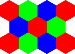
By combining these figures, you can get a “breadboard” that is interesting from the point of view of art rather than practice :

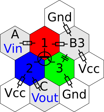
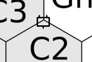
It is interesting to make a "cellular" board so that the circuit can be assembled regardless of the pin order of the three-pin component. Pads marked with red (1), green (2) and blue (3) colors go to the component soldering point in the SOT23-3 housing located at the bottom, pads marked with letters A, B, C with numbers and also with Vcc and Gnd, connect the board to external circuits through small additional pads to which you can solder the comb. Since all the sites of the same name (A, B, C, Vcc, GND) are interconnected, there are only five conclusions at the comb. The sites marked in white are originally designed to supply power, but their role can be reassigned. Please also note that the sites marked in gray have two alphanumeric designations: one on top, the other on the bottom.
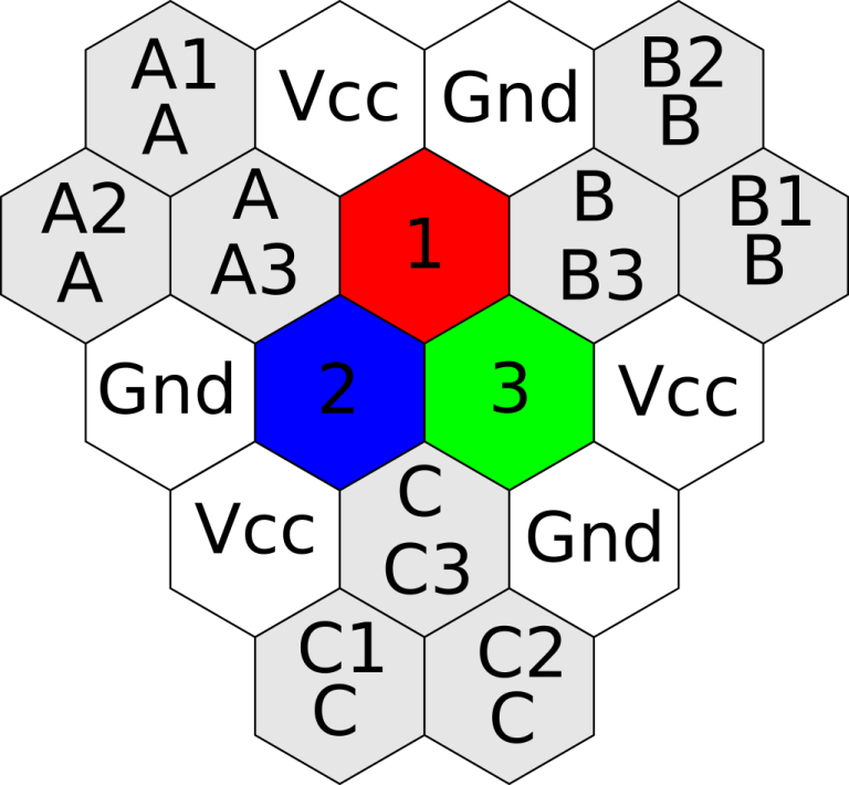
As “bridges” between any two adjacent sites, two-pin SMD components in 0603 cases can be used. These can be resistors, ceramic capacitors, diodes, even small inductors, etc. Also, there are jumpers in such cases, but they are easier to make from pieces of hard tinned wire.
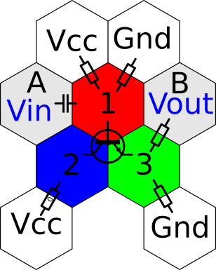
There are a lot of options for circuits that can be assembled on such a board. For example, an emitter follower:
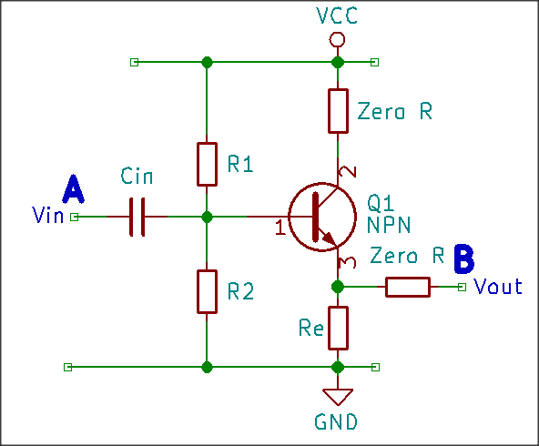
Turns into:
Cascade with voltage boost:

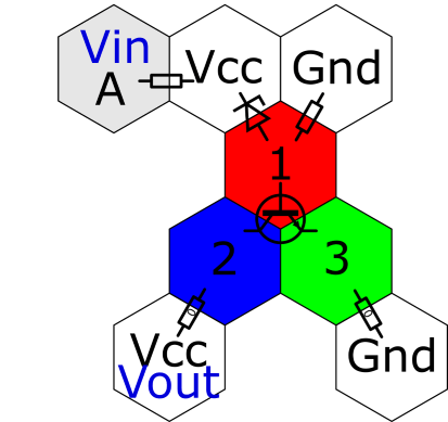
It is on the board:
Parametric stabilizer:

On the board, comb contacts are used non-standard: A - input, Vcc - output:
Phase shifting generator:
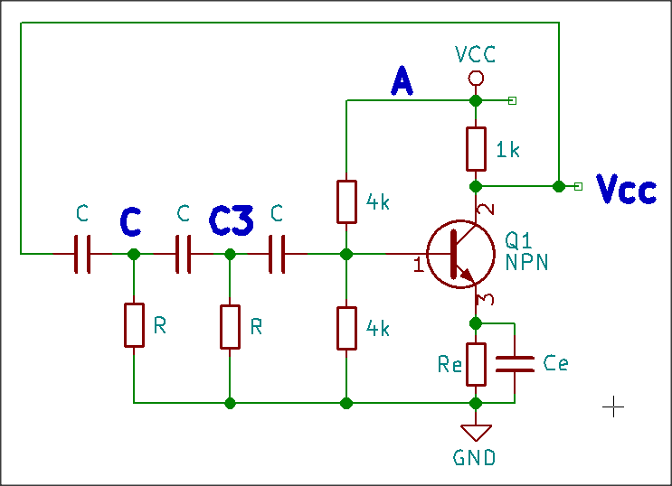
On the board, non-standard use of pads again: A - power , Vcc - output:

The author designed the following board drawing:

And imagined what it would look like if you stuffed it with components to the eyeballs: The

necessary files in the KiCAD format are here under the GPL v3.
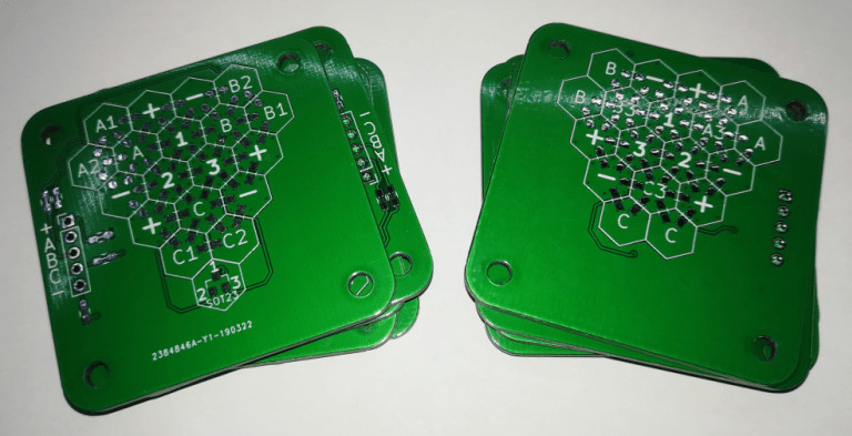
And so the boards came from China for $ 2 for 10 pieces:
From a translator: it would be better to make the “honeycombs” much smaller, fill them with the entire space of the board, not connect them to each other, do not cover anything with silk-screen printing, on combs and specials. a place for SOT23-3 to display nothing and not to provide for them at all. SOT23-3 can be soldered directly to three any pads somehow like this:
It is clear that in this case it will be necessary to place not only components on the board, but also jumpers of arbitrary shape, as on ordinary prototyping boards. The advantage of being able to solder up to six SMD components to a single pad is retained.