Using the Datapath Config Tool
We have to take the penultimate step in the practical development of working with UDB. Today we will conduct development not using the automated UDB Editor, but in a semi-manual mode using the Datapath Config Tool. A very good help in mastering this tool is AN82156 - PSoC 3, PSoC 4, and PSoC 5LP - Designing PSoC Creator Components with UDB Datapaths. Actually, I studied it myself.
Perhaps, when reading our translations of documentation on UDB, someone tried to reproduce the knowledge from there into practice and noticed that not all the functionality described in the publications is available in the UDB Editor. This is due to the fact that the developers did not begin to place some particularly cumbersome mechanisms in the UDB Editor. The authors of AN82156 argue that through the UDB Editor you can’t do the following things:
- organize parallel data input and output;
- organize dynamic FIFO management;
- implement the inverse of the FIFO clock signal;
- implement the CRC function;
- implement the PRS function;
- implement the choice of incoming transfer;
- implement dynamic inbound migration.
From myself, I will add that I did not find how to implement the permutation of nibbles in the UDB Editor.
If these functions are necessary in the project, you will need to create your own Verilog code. I specifically used the word "create" rather than "write." To know this programming language is enough at the reading level. I mean, you need to understand what design is needed for what. And to be able to write from scratch is always useful, but this skill is not required for what is presented in this article.
As a solvable problem, I chose a semi-synthetic case. In general, I decided to output some data to the parallel port, and in particular, from what is at hand, the text LCD has a parallel port. I pulled it out of the MZ3D 3D printer three years ago when I transplanted the latter to STM32. Therefore, the case is semi-synthetic: today, such indicators usually have an I2C input, and they do not need to connect through a pile of wires in real life. However, modern LCDs also have parallel ports, so everyone can use them to repeat the experiment.
Consider the display switching scheme taken from reprap.org (this was not easy, my provider blocks this site, as well as a number of other technical ones, explaining that he lives on the same IP as someone blocked).

Great layout! Firstly, I don’t have to think about reading: data in the LCD can only be written (the R / W line is grounded and not available on the connector). Secondly, the data comes in a 4-bit format, which means that we can not only work out the parallel output, but also check the operation of the nibble permutation function.
Project creation
So, launch PSoC Creator and select File-> New-> Project :

Next, I select my breadboard:
Next - an empty diagram: I
will name the project LCDTest2 :
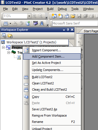
Now, as before, go to the Components tab :

And, having selected the project, click the right button “Mice”, then select Add Component Item .
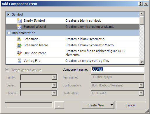
And here you have to choose the Symbol Wizard . Let 's give a name ... Well, let's say LCD4bit .
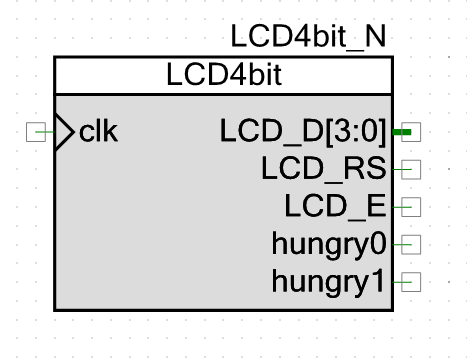
I assigned the following ports to the symbol:

clk is the clock input. Ports with an LCD prefix are standard LCD ports. hungry- the outputs informing the DMA unit that there is free space in the FIFO, the idea was considered in the article about controlling RGB LEDs . Click OK to get the character.
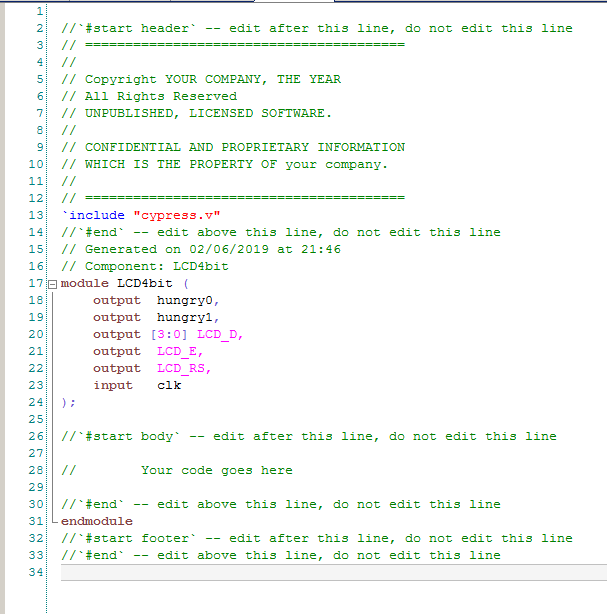
Now, based on this symbol, a Verilog template should be generated. Press the right mouse button in the vicinity of the symbol and select Generate Verilog in the context menu .

We got the template shown in the figure below (in text form it does not make any sense yet):
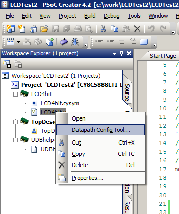
We have created a module and some sections. But they have not created Datapath yet. To add it, go to the project tree, select the LCD4bit.v file , press the right mouse button and select the Datapath Config Tool in the context menu that appears :

A window opens before us, which I will only partially show for now:

Please love and favor, Datapath editor. It contains all the bits that were described in the translation of proprietary documentation. But there are so many of these bits that in the early days I looked at him, but was afraid to do something. Look, look and go out. And only after some time, getting used to it, he began to try to do something. Actually, that's why I brought only part of the window. Why scare everyone ahead of time? In the meantime, we just need to create a Datapath, so we select the menu item Edit-> New Datapath :
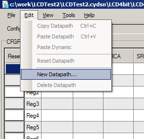
Which option should I choose in the dialog that appears?
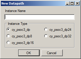
The question is a little more serious than it seems. Let me even single out the next paragraph so that no one gets caught (I caught myself, and then I saw questions on the network from the ones I got, and no one really answered them, and the answer is in AN82156 , you just need to read it diagonally, as it says there short inconspicuous phrase).
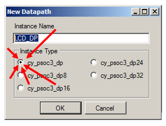
If you plan to work with parallel data, you must definitely choose the option CY_PSOC3_DP. No other option will contain ports for connecting parallel data.So. Let us call the instance LCD_DP:
Click OK and close the Datapath Config Tool for now , agreeing to save the result. We will come back here later.
Our Verilog code has expanded. Now it has Datapath. His beginning is completely unreadable. It's not scary, it is configured by the Datapath Config Tool .
And we will rule the end of the Datapath description. Our site looks like this
(from this point it makes sense to bring everything in text form).
)) LCD_DP(
        /*  input                   */  .reset(1'b0),
        /*  input                   */  .clk(1'b0),
        /*  input   [02:00]         */  .cs_addr(3'b0),
        /*  input                   */  .route_si(1'b0),
        /*  input                   */  .route_ci(1'b0),
        /*  input                   */  .f0_load(1'b0),
        /*  input                   */  .f1_load(1'b0),
        /*  input                   */  .d0_load(1'b0),
        /*  input                   */  .d1_load(1'b0),
        /*  output                  */  .ce0(),
        /*  output                  */  .cl0(),
        /*  output                  */  .z0(),
        /*  output                  */  .ff0(),
        /*  output                  */  .ce1(),
        /*  output                  */  .cl1(),
        /*  output                  */  .z1(),
        /*  output                  */  .ff1(),
        /*  output                  */  .ov_msb(),
        /*  output                  */  .co_msb(),
        /*  output                  */  .cmsb(),
        /*  output                  */  .so(),
        /*  output                  */  .f0_bus_stat(),
        /*  output                  */  .f0_blk_stat(),
        /*  output                  */  .f1_bus_stat(),
        /*  output                  */  .f1_blk_stat(),
        /* input                    */  .ci(1'b0),     // Carry in from previous stage
        /* output                   */  .co(),         // Carry out to next stage
        /* input                    */  .sir(1'b0),    // Shift in from right side
        /* output                   */  .sor(),        // Shift out to right side
        /* input                    */  .sil(1'b0),    // Shift in from left side
        /* output                   */  .sol(),        // Shift out to left side
        /* input                    */  .msbi(1'b0),   // MSB chain in
        /* output                   */  .msbo(),       // MSB chain out
        /* input [01:00]            */  .cei(2'b0),    // Compare equal in from prev stage
        /* output [01:00]           */  .ceo(),        // Compare equal out to next stage
        /* input [01:00]            */  .cli(2'b0),    // Compare less than in from prv stage
        /* output [01:00]           */  .clo(),        // Compare less than out to next stage
        /* input [01:00]            */  .zi(2'b0),     // Zero detect in from previous stage
        /* output [01:00]           */  .zo(),         // Zero detect out to next stage
        /* input [01:00]            */  .fi(2'b0),     // 0xFF detect in from previous stage
        /* output [01:00]           */  .fo(),         // 0xFF detect out to next stage
        /* input [01:00]            */  .capi(2'b0),   // Software capture from previous stage
        /* output [01:00]           */  .capo(),       // Software capture to next stage
        /* input                    */  .cfbi(1'b0),   // CRC Feedback in from previous stage
        /* output                   */  .cfbo(),       // CRC Feedback out to next stage
        /* input [07:00]            */  .pi(8'b0),     // Parallel data port
        /* output [07:00]           */  .po()          // Parallel data port
);
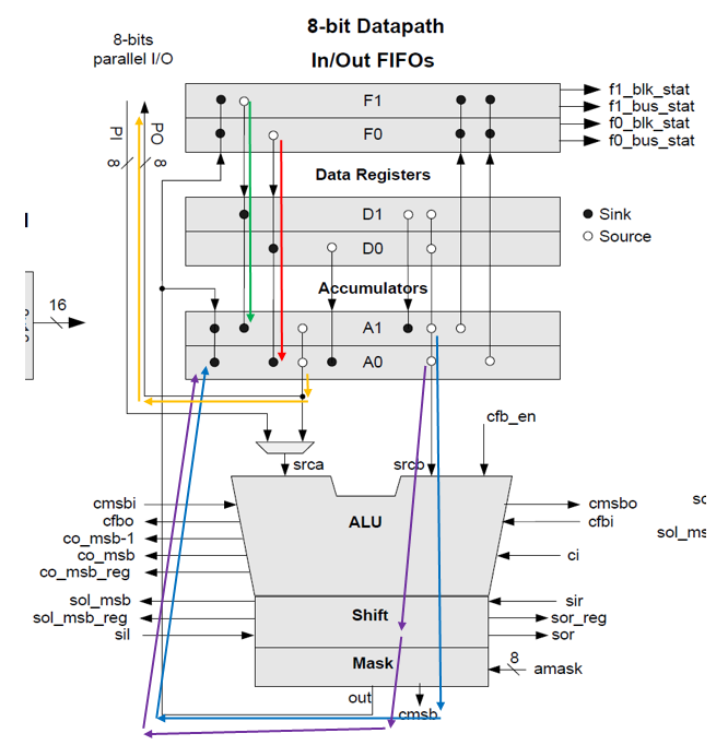
Scary? Now we’ll figure out what's what - it’ll cease to be scary. In fact, there are three distinct groups in this text. Let's recall the translation of the documentation. What did the datapath look like in the picture? I will immediately note in the figure the places to which the groups “1”, “2” and “3” belong.
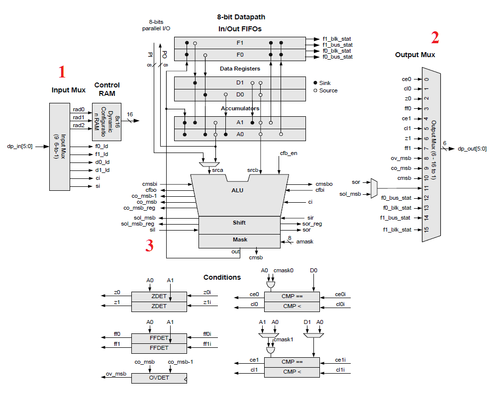
Actually, the first group of ports in verilog code is the inputs. Compare the names at the output of the input multiplexer (“1” in the figure) and the names of the signals in the code.
Now all the inputs are zero. We will have to connect a clock input and we can forward up to six input lines, as was done in the UDB Editor. These inputs are:
        /*  input                   */  .reset(1'b0),
        /*  input                   */  .clk(1'b0),
        /*  input   [02:00]         */  .cs_addr(3'b0),
        /*  input                   */  .route_si(1'b0),
        /*  input                   */  .route_ci(1'b0),
        /*  input                   */  .f0_load(1'b0),
        /*  input                   */  .f1_load(1'b0),
        /*  input                   */  .d0_load(1'b0),
        /*  input                   */  .d1_load(1'b0),
The second group is the exits. The names in the code also match the names of the inputs of the output multiplexer "2":
        /*  output                  */  .ce0(),
        /*  output                  */  .cl0(),
        /*  output                  */  .z0(),
        /*  output                  */  .ff0(),
        /*  output                  */  .ce1(),
        /*  output                  */  .cl1(),
        /*  output                  */  .z1(),
        /*  output                  */  .ff1(),
        /*  output                  */  .ov_msb(),
        /*  output                  */  .co_msb(),
        /*  output                  */  .cmsb(),
        /*  output                  */  .so(),
        /*  output                  */  .f0_bus_stat(),
        /*  output                  */  .f0_blk_stat(),
        /*  output                  */  .f1_bus_stat(),
        /*  output                  */  .f1_blk_stat(),
Only the given Datapath species has the third group (the others have none, therefore, there are no parallel data). These are internal Datapath signals through which you can independently chain together or perform other useful actions. The names in the code also coincide with the names of the internal signals scattered in the figure. We through one of them (the last in the list, his name is po ) will output parallel data directly to the legs of the chip.
        /* input                    */  .ci(1'b0),     // Carry in from previous stage
        /* output                   */  .co(),         // Carry out to next stage
        /* input                    */  .sir(1'b0),    // Shift in from right side
        /* output                   */  .sor(),        // Shift out to right side
        /* input                    */  .sil(1'b0),    // Shift in from left side
        /* output                   */  .sol(),        // Shift out to left side
        /* input                    */  .msbi(1'b0),   // MSB chain in
        /* output                   */  .msbo(),       // MSB chain out
        /* input [01:00]            */  .cei(2'b0),    // Compare equal in from prev stage
        /* output [01:00]           */  .ceo(),        // Compare equal out to next stage
        /* input [01:00]            */  .cli(2'b0),    // Compare less than in from prv stage
        /* output [01:00]           */  .clo(),        // Compare less than out to next stage
        /* input [01:00]            */  .zi(2'b0),     // Zero detect in from previous stage
        /* output [01:00]           */  .zo(),         // Zero detect out to next stage
        /* input [01:00]            */  .fi(2'b0),     // 0xFF detect in from previous stage
        /* output [01:00]           */  .fo(),         // 0xFF detect out to next stage
        /* input [01:00]            */  .capi(2'b0),   // Software capture from previous stage
        /* output [01:00]           */  .capo(),       // Software capture to next stage
        /* input                    */  .cfbi(1'b0),   // CRC Feedback in from previous stage
        /* output                   */  .cfbo(),       // CRC Feedback out to next stage
        /* input [07:00]            */  .pi(8'b0),     // Parallel data port
        /* output [07:00]           */  .po()          // Parallel data port
);
So. As we work, we will have to connect some of these inputs and outputs to our own entities, and the rest - just leave them in the form in which we created them.
Using UDB Editor as a reference
And now we have a blank, we know where and what we have to write. It remains to understand what exactly we will enter there. It so happened that I do not use the Verilog language every day, so in general terms I remember everything, and writing from scratch for me is always a stressful situation. When the project is already underway, it is all remembered, but if after a couple of months of inactivity I start something from scratch, of course, I no longer remember the syntax details of this particular language. Therefore, I suggest asking the development environment to help us.
UDB Editor for self-monitoring builds Verilog code. We take advantage of the fact that components that are not involved in the main circuit are not compiled, so we can create an auxiliary component in the UDB Editor, and it will not get into the output code. We will draw an automaton there, we will make a rough adjustment of the Datapath inputs and outputs, and then just transfer the automatically generated text to our verilog module and modify everything creatively. This is much simpler than remembering Verilog syntax details and writing everything from scratch (although whoever constantly uses Verilog will certainly be easier to write from scratch: creative completion, as we will soon see, is simple, but requires time).
So, we begin to make an auxiliary component. With the usual movement of the hand we add a new element to the project:

This will be a UDB document, let's call it UDBhelper :

It's time to think about the automaton, which we will place on the created sheet. To do this, we need to consider what time diagram we should form with it:
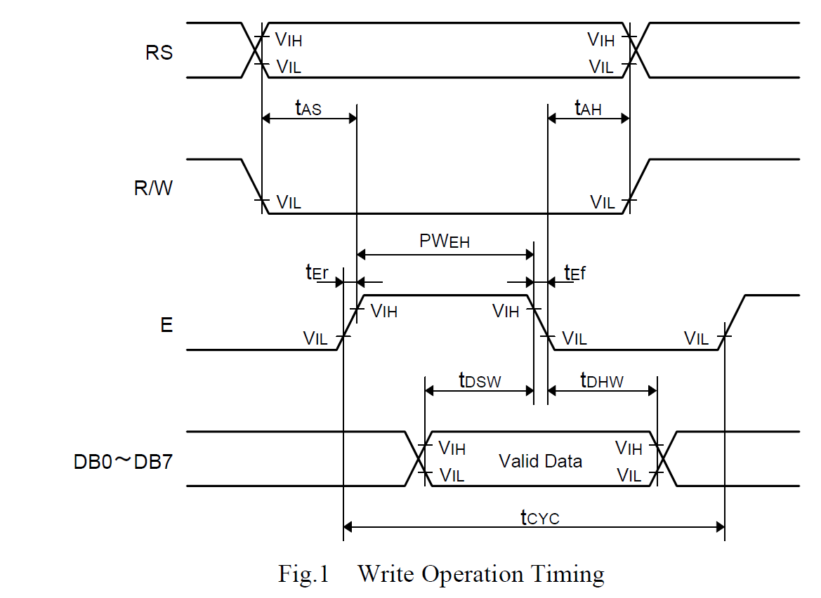
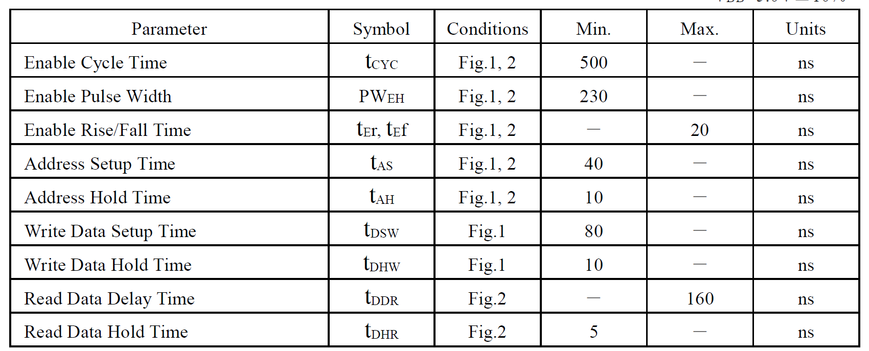
So. First you need to set the RS signal (since R / W is soldered to zero in hardware). Next, wait for tAS, and then raise the signal E and set the data (setting data on the positive edge of E is not limited). The data must be on the bus no less than tDSW, then the signal E must be dropped. The data must remain on the bus for at least tDHW, and RS for at least tAH.
RS is the command or data flag. If RS is zero, then a command is written, if one is data.
I offer through FIFO0send commands, and through FIFO1 - data. In the framework of the current task, this does not contradict anything. Then the state machine proposed by me will have the following form:
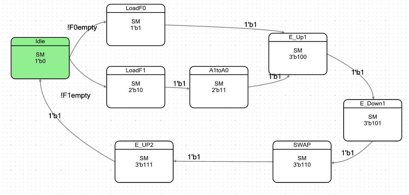
In the Idle state, the machine is located while there is no data in any of the FIFOs. If data appeared in FIFO0 , it goes to LoadF0 state , where in the future it will receive data from FIFO0 to A0.
While the commands are being transmitted, the data should not be sent. Therefore, the condition for receiving data will be lower in priority than the condition for receiving commands.
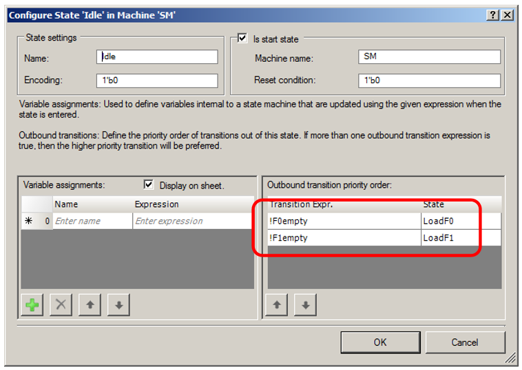
Data is received in A1 in state LoadF1 (from FIFO1they can only go to register A1 and cannot go to register A0), and then are copied from A1 to A0 in the state A1toA0 .
Whatever way we go to the point of convergence of the arrows, we have data in A0. They are already output to the parallel port. We cock E (in state E_UP1 ), drop E (in state E_DOWN1 ). Next, we will have a state for swapping nibbles ( SWAP ), after which E rises again ( E_UP2 ). On this, I have exhausted eight states that can be encoded in three bits. And we remember that the Datapath dynamic configuration RAM has only three address inputs. Some tricks could be applied, but the article is already big. Therefore, just the second time we will drop E in the stateIdle . Then eight states are quite enough for us.
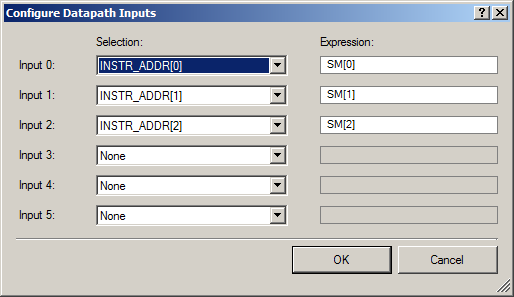
We also put Datapath on the sheet and assign its inputs and outputs in a way that is familiar in the previous articles. Here are the inputs:
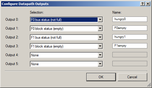
Here are the outputs:
Nothing new, everything has already been described in previous articles of the cycle. So, we have a blank, based on which we can do something of our own. True, in order to make sure that everything is going, we need to bring our system to the top level of the project, otherwise no errors will be found. And in the initial experiments without errors will fail. Therefore, we will do one more auxiliary action.
The description of how the circuit is made goes beyond the description of working with UDB. I’ll just show you which circuit I got. There is only one DMA unit: when sending commands to the LCD, it is necessary to withstand large pauses, so it is still easier to do this programmatically. For other applications, you can simply put the second DMA block by analogy using the hungry0 signal .

To precisely meet the time frame, I chose a clock frequency equal to one megahertz. It would be possible to take a frequency and higher, but the data is transmitted over long wires in conditions of high interference, so the time to set the data before and after the strobe is better to take with a margin. If someone will repeat my experiments on the same breadboard - do not use port P3.2: a capacitor is soldered to this leg on the board. I killed for half an hour, until I discovered why I did not form an impulse E, which I first connected there. I threw it to P3.1 - it all worked right away. My data bus goes to P3.7-P3.4, RS goes to P3.3, so E originally went to P3.2 ...
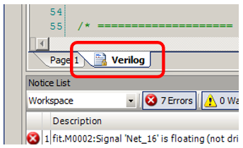
Well. Now, if you try to compile the project, we get quite predictable errors

So the system is trying to collect something. But she still has nothing to collect. We proceed to copy the code. To do this, switch to the Verilog tab in the UDB Editor (this tab is located under the window with the UDB Editor sheet):
What is familiar there? At the very end of the text is the body of the automaton. Let's start the migration from it.
Also place it under Datapath:
/* ==================== State Machine: SM ==================== */
always @ (posedge clock)
begin : Idle_state_logic
    case(SM)
        Idle :
        begin
            if (( !F0empty ) == 1'b1)
            begin
                SM <= LoadF0 ;
            end
            else if (( !F1empty ) == 1'b1)
            begin
                SM <= LoadF1 ;
            end
        end
        LoadF0 :
        begin
            if (( 1'b1 ) == 1'b1)
            begin
                SM <= E_Up1 ;
            end
        end
        E_Up1 :
        begin
            if (( 1'b1 ) == 1'b1)
            begin
                SM <= E_Down1 ;
            end
        end
        E_Down1 :
        begin
            if (( 1'b1 ) == 1'b1)
            begin
                SM <= SWAP ;
            end
        end
        SWAP :
        begin
            if (( 1'b1 ) == 1'b1)
            begin
                SM <= E_UP2 ;
            end
        end
        E_UP2 :
        begin
            if (( 1'b1 ) == 1'b1)
            begin
                SM <= Idle ;
            end
        end
        LoadF1 :
        begin
            if (( 1'b1 ) == 1'b1)
            begin
                SM <= A1toA0 ;
            end
        end
        A1toA0 :
        begin
            if (( 1'b1 ) == 1'b1)
            begin
                SM <= E_Up1 ;
            end
        end
        default :
        begin
            SM <= Idle;
        end
    endcase
end
There are declarations at the top for this code (names for states, chains for Datapath, a register encoding the state of an automaton). We transfer them to the appropriate
section of our code:
/* ==================== Wire and Register Declarations ==================== */
localparam [2:0] Idle = 3'b000;
localparam [2:0] LoadF0 = 3'b001;
localparam [2:0] LoadF1 = 3'b010;
localparam [2:0] E_Up1 = 3'b100;
localparam [2:0] A1toA0 = 3'b011;
localparam [2:0] E_Down1 = 3'b101;
localparam [2:0] SWAP = 3'b110;
localparam [2:0] E_UP2 = 3'b111;
wire hungry0;
wire F0empty;
wire hungry1;
wire F1empty;
wire Datapath_1_d0_load;
wire Datapath_1_d1_load;
wire Datapath_1_f0_load;
wire Datapath_1_f1_load;
wire Datapath_1_route_si;
wire Datapath_1_route_ci;
wire  [2:0] Datapath_1_select;
reg  [2:0] SM;
Well
the signal binding site is transferable:
/* ==================== Assignment of Combinatorial Variables ==================== */
assign Datapath_1_d0_load = (1'b0);
assign Datapath_1_d1_load = (1'b0);
assign Datapath_1_f0_load = (1'b0);
assign Datapath_1_f1_load = (1'b0);
assign Datapath_1_route_si = (1'b0);
assign Datapath_1_route_ci = (1'b0);
assign Datapath_1_select[0] = (SM[0]);
assign Datapath_1_select[1] = (SM[1]);
assign Datapath_1_select[2] = (SM[2]);
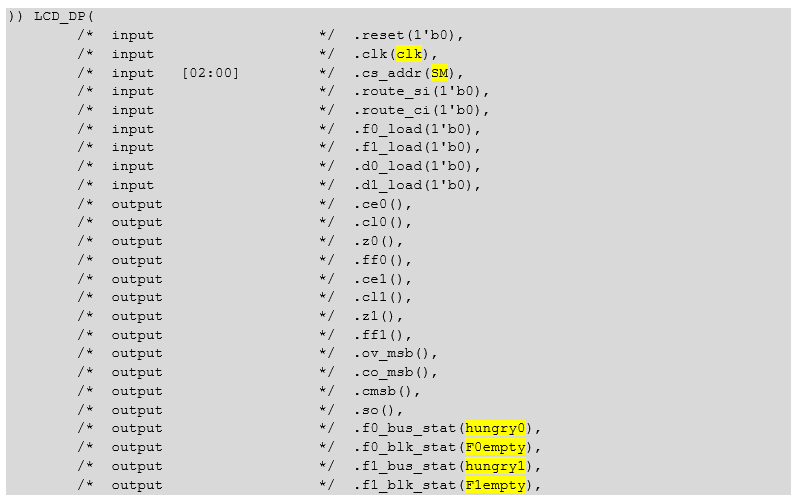
It's time to plug in Datapath. The code ported from the UDB Editor is good for machine editing, but not very good for manual editing. There, chains are created that connect to the Datapath inputs at one end and to constants at the other. But in the code created by the Datapath Configuration Tool (which does everything for manual work), all inputs are already directly connected to zero constants. So I’ll connect only those lines that are not constants, but I’ll cut out everything related to the forwarding of constants from the transferred text. The connection turned out like this (the color highlights the places that I edited regarding the automatically created in the Datapath Configuration Tool):
Same text:
)) LCD_DP(
        /*  input                   */  .reset(1'b0),
        /*  input                   */  .clk(clk),
        /*  input   [02:00]         */  .cs_addr(SM),
        /*  input                   */  .route_si(1'b0),
        /*  input                   */  .route_ci(1'b0),
        /*  input                   */  .f0_load(1'b0),
        /*  input                   */  .f1_load(1'b0),
        /*  input                   */  .d0_load(1'b0),
        /*  input                   */  .d1_load(1'b0),
        /*  output                  */  .ce0(),
        /*  output                  */  .cl0(),
        /*  output                  */  .z0(),
        /*  output                  */  .ff0(),
        /*  output                  */  .ce1(),
        /*  output                  */  .cl1(),
        /*  output                  */  .z1(),
        /*  output                  */  .ff1(),
        /*  output                  */  .ov_msb(),
        /*  output                  */  .co_msb(),
        /*  output                  */  .cmsb(),
        /*  output                  */  .so(),
        /*  output                  */  .f0_bus_stat(hungry0),
        /*  output                  */  .f0_blk_stat(F0empty),
        /*  output                  */  .f1_bus_stat(hungry1),
        /*  output                  */  .f1_blk_stat(F1empty),
Parallel data is a bit more complicated. Datapath has an eight-bit port, and only four of them need to be brought out. Therefore, we start the auxiliary circuit and connect only half of it to the output:
wire [7:0] tempBus;
assign LCD_D = tempBus[7:4];
And connect it like this:

Same text:
      /* input [07:00]      */  .pi(8'b0),     // Parallel data port
      /* output [07:00]     */  .po( tempBus)   // Parallel data port
);
We try to assemble (Shift + F6 or through the menu item Build-> Generate Application ). We
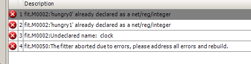
get the error: We have the ports hungry0 and hungry1 (appeared when creating the component), as well as the chains of the same name (appeared when dragging from the sample). Just remove these chains (leaving the ports). And somewhere the clock signal leaked , and we have this circuit called clk .
After removing all unnecessary circuits (those that initially threw zero constants to the Datapath inputs, as well as hungry0 and hungry1 ), we get the following code for the beginning of our file:
//        Your code goes here
/* ==================== Wire and Register Declarations ==================== */
localparam [2:0] Idle    = 3'b000;
localparam [2:0] LoadF0  = 3'b001;
localparam [2:0] LoadF1  = 3'b010;
localparam [2:0] E_Up1   = 3'b100;
localparam [2:0] A1toA0  = 3'b011;
localparam [2:0] E_Down1 = 3'b101;
localparam [2:0] SWAP    = 3'b110;
localparam [2:0] E_UP2   = 3'b111;
wire F0empty;
wire F1empty;
reg  [2:0] SM;
/* ==================== Assignment of Combinatorial Variables ==================== */
wire [7:0] tempBus;
assign LCD_D = tempBus[7:4];
And when replacing clock with clk in the body of the machine, at the same time I will throw out all the lines that are good for auto-generation, but with manual editing only create confusion (all comparisons that give an unconditional result TRUE and so on). In particular, in the example below, you can cross out about half of the lines (and some begin / end are optional, sometimes they will be needed, because we will add actions, I highlighted them):
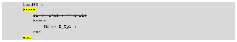
After combing according to the above principle (and replacing clock with clk ) such a body remains
(it has become shorter, which means it is easier to read):
always @ (posedge clk)
begin : Idle_state_logic
    case(SM)
        Idle :
        begin
            if (( !F0empty ) == 1'b1)
            begin
                SM <= LoadF0 ;
            end
            else if (( !F1empty ) == 1'b1)
            begin
                SM <= LoadF1 ;
            end
        end
        LoadF0 :
        begin
            SM <= E_Up1 ;
        end
        E_Up1 :
        begin
            SM <= E_Down1 ;
        end
        E_Down1 :
        begin
            SM <= SWAP ;
        end
        SWAP :
        begin
            SM <= E_UP2 ;
        end
        E_UP2 :
        begin
            SM <= Idle ;
        end
        LoadF1 :
        begin
            SM <= A1toA0 ;
        end
        A1toA0 :
        begin
            SM <= E_Up1 ;
        end
        default :
        begin
            SM <= Idle;
        end
    endcase
end
Now, during compilation, we are told that the LCD_E and LCD_RS circuits are not connected.
Actually, this is true:

It's time to add a finite state machine. We will replace the declarations of the ports corresponding to the unconnected chains with reg , since we will write in them in the body of the machine (this is the syntax of the Verilog language, if we write, the data should click in, for this we need a trigger, and it is given by the keyword reg ):
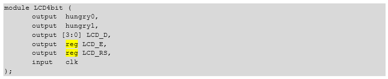
Same text:
module LCD4bit (
	output  hungry0,
	output  hungry1,
	output [3:0] LCD_D,
	output  reg LCD_E,
	output  reg LCD_RS,
	input   clk
);
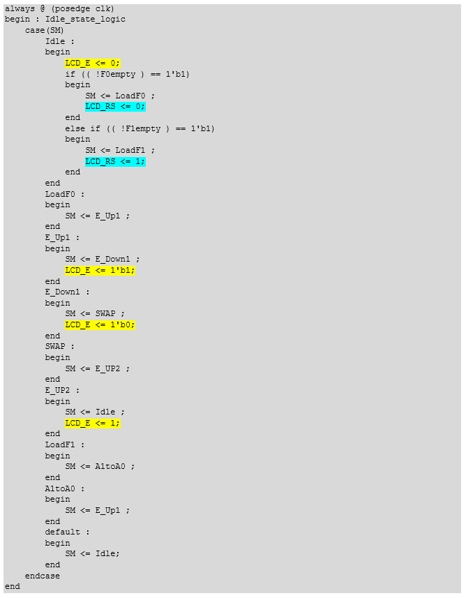
And fill the machine with actions. I already spoke the logic above when I was considering the transition graph of the automaton, so I will only show the result:
Same text:
always @ (posedge clk)
begin : Idle_state_logic
    case(SM)
        Idle :
        begin
            LCD_E <= 0;
            if (( !F0empty ) == 1'b1)
            begin
                SM <= LoadF0 ;
                LCD_RS <= 0;
            end
            else if (( !F1empty ) == 1'b1)
            begin
                SM <= LoadF1 ;
                LCD_RS <= 1;
            end
        end
        LoadF0 :
        begin
            SM <= E_Up1 ;
        end
        E_Up1 :
        begin
            SM <= E_Down1 ;
            LCD_E <= 1'b1;
        end
        E_Down1 :
        begin
            SM <= SWAP ;
            LCD_E <= 1'b0;
        end
        SWAP :
        begin
            SM <= E_UP2 ;
        end
        E_UP2 :
        begin
            SM <= Idle ;
            LCD_E <= 1;
        end
        LoadF1 :
        begin
            SM <= A1toA0 ;
        end
        A1toA0 :
        begin
            SM <= E_Up1 ;
        end
        default :
        begin
            SM <= Idle;
        end
    endcase
end
From this moment, the project begins to assemble. But he will not work yet. So far I have famously said: “In this state, we will load the register from FIFO”, “A1 will copy into A0 in this”, “Nibbles will be swapped in this”. In general, I spoke a lot, but so far there have been no actions. The time has come to fulfill them. We look at how the states were encoded:
localparam [2:0] Idle    = 3'b000;
localparam [2:0] LoadF0  = 3'b001;
localparam [2:0] LoadF1  = 3'b010;
localparam [2:0] E_Up1   = 3'b100;
localparam [2:0] A1toA0  = 3'b011;
localparam [2:0] E_Down1 = 3'b101;
localparam [2:0] SWAP    = 3'b110;
localparam [2:0] E_UP2   = 3'b111;
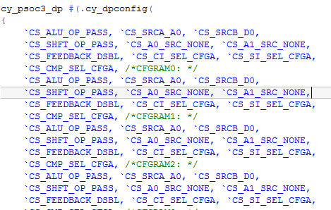
Rediscover Datapath the Configuration Tool will :
And start to edit a line CFGRAM . When editing, you should keep in mind the Datapath scheme, namely: With the red
frames in the figure below (and with the arrows in the figure above) I highlighted the corrected areas (and the data path) for the state LoadF0 (code 001, that is, Reg1 ). I also entered comments manually. The contents of F0 should get into A0.
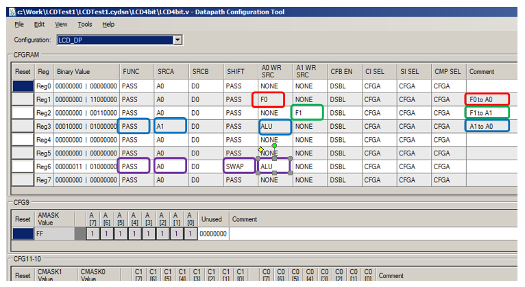
With green frames and arrows I marked the settings and the path for the state LoadF1 (code 010 - Reg2 ).
With blue frames and arrows I marked the settings and the path for the state A1toA0 (code 011 - Reg3 ).
The purple frames and arrows I marked the settings and path for the state of SWAP (code 110 - Reg6 ).
Finally, the orange arrows show the parallel data path. And no action is taken for them. They always come out of the SRCA . We almost always have A0 selected as SRCA : data comes out of A0. So, to redirect the input data, we would have to carry out a lot of auxiliary actions, but we do not accept any data, so here we do not need these actions, and everyone will find their list in AN82156 . We also do not need to edit any static Datapath settings, so close the Datapath Config Tool .
Everything. Conceived hardware completed. Getting started developing C code. To do this, go to the Source tab and edit the main.c file .

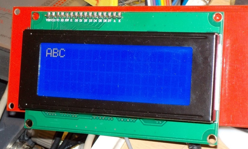
Regular LCD initialization and “ABC” character output look like this (I remind you that the commands go to FIFO0 , the documentation needs to insert pauses between the teams, and the data goes to FIFO1 , I did not find anything about the pauses between the data):
    volatile uint8_t* pFIFO0 = (uint8_t*) LCD4bit_1_LCD_DP__F0_REG;
    volatile uint8_t* pFIFO1 = (uint8_t*) LCD4bit_1_LCD_DP__F1_REG;
    pFIFO0[0] = 0x33;
    CyDelay (5);
    pFIFO0[0] = 0x33;
    CyDelay (100);
    pFIFO0[0] = 0x33;
    CyDelay (5);
    pFIFO0[0] = 0x20;
    CyDelay (5);
    pFIFO0[0] = 0x0C;       // включили экран
    CyDelay (50);
    pFIFO0[0] = 0x01;      // Очистили экран
    CyDelay (50);
    pFIFO1[0] = 'A';
    pFIFO1[0] = 'B';
    pFIFO1[0] = 'C';
What? Why is there only the first character on the screen?

And if you add delays between the output of the data, everything is fine: the
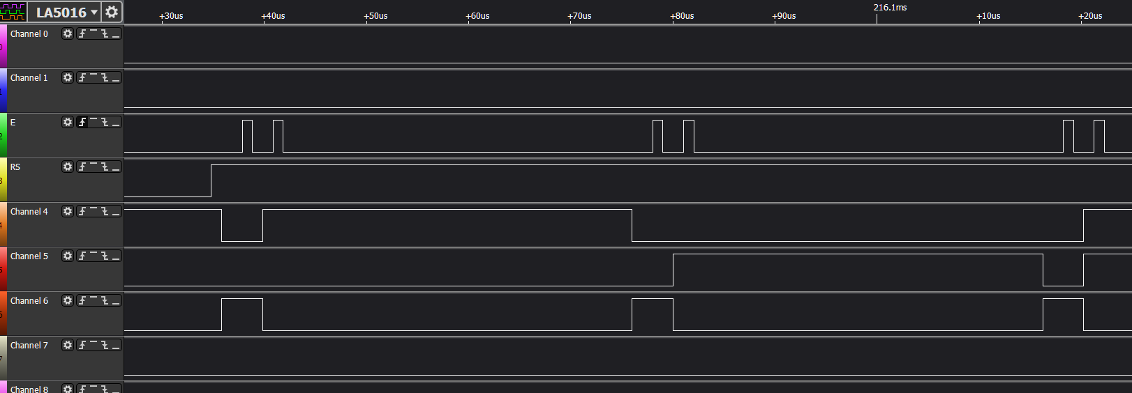
oscilloscope will not have enough channels for such work. We check the work on a logical analyzer. The data recording process is as follows.
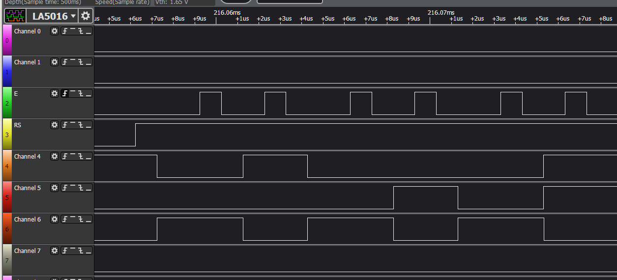
All data is in place (three pairs of packages). Time for installation and snapping data is allocated in sufficient volume. In general, from the point of view of time diagrams - everything is done correctly. The scientific problem is solved, the desired time diagrams are formed. Here is engineering - no. The reason for this is the slowness of the processor installed in the LCD. Between bytes, add delays.
We will form delays with the help of a seven-bit counter, at the same time we will train to add it to such a system. Let us be in the Idle state for no less than some given time, and a seven-bit counter will measure this time for us. And again, we will not write, but create code. Therefore, again we go to the auxiliary component of the UDB Editor and add a counter to the sheet, setting its parameters as follows:
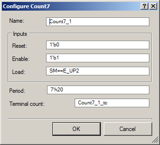
This counter will always work ( Enable is set to 1). But it will load when the machine is in the E_UP2 state (after which we immediately fall into the Idle state ). Line Count7_1_tccocked to 1 when the counter counts to zero, which we will make an additional condition for exiting the Idle state . The figure also contains the value of the period, but we will not find it in the Verilog code. It will have to be entered into the C code. But first, we transfer the automatically generated Verilog code by switching to the Verilog tab. First of all, the counter should be connected (we see this code at the beginning of the file and move it to the beginning too):
`define CY_BLK_DIR "$CYPRESS_DIR\..\psoc\content\CyComponentLibrary\CyComponentLibrary.cylib\Count7_v1_0"
`include "$CYPRESS_DIR\..\psoc\content\CyComponentLibrary\CyComponentLibrary.cylib\Count7_v1_0\Count7_v1_0.v"
How the creative refinement of lines and constants is performed has already been described, so I'll just show the result. Here are the chains and assignments added as a result (the rest set the constants, so I threw them away):
wire Count7_1_load;
wire Count7_1_tc;
assign Count7_1_load = (SM==E_UP2);
And here is the counter itself, placed at the end of the file. All constants are assigned to ports directly in this declaration:
    Count7_v1_0 Count7_1 (
        .en(1'b1),
        .load(Count7_1_load),
        .clock(clk),
        .reset(1'b0),
        .cnt(),
        .tc(Count7_1_tc));
    defparam Count7_1.EnableSignal = 1;
    defparam Count7_1.LoadSignal = 1;
To enable this counter to work, we automatically add an additional condition for exiting the Idle state :
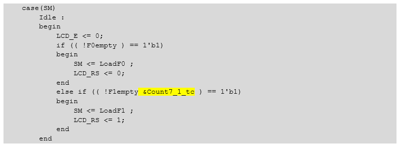
Same text:
    case(SM)
        Idle :
        begin
            LCD_E <= 0;
            if (( !F0empty ) == 1'b1)
            begin
                SM <= LoadF0 ;
                LCD_RS <= 0;
            end
            else if (( !F1empty &Count7_1_tc ) == 1'b1)
            begin
                SM <= LoadF1 ;
                LCD_RS <= 1;
            end
        end
The API for the counter added in this way is not created, so we add two magic lines to the main function , which I formed in the image and likeness seen in the API from past projects (the first line sets the loaded value of the account, the same Load, the second starts the counter):
    *((uint8_t*)LCD4bit_1_Count7_1_Counter7__PERIOD_REG) = 0x20;
    *((uint8_t*)LCD4bit_1_Count7_1_Counter7__CONTROL_AUX_CTL_REG) |= 0x20;   // Start
The analyzer shows that in the modified case there is a delay: the
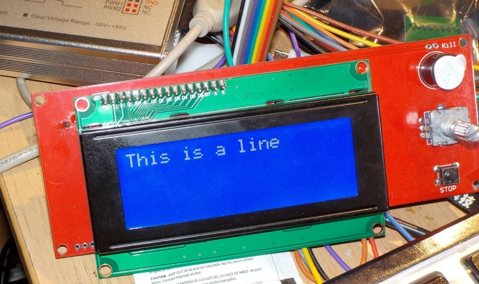
LCD also has all three characters.
But programmatic character output in real life is unacceptable. Just adding them to FIFO will overflow. Wait for the FIFO to empty - this means creating large delays for the processor core. The processor operates at a frequency of 72 MHz, and data is output for 7-8 clock cycles at a frequency of 1 MHz. Therefore, in real life, the text must be displayed using DMA. This is where the “Launch and Forgot” principle comes in handy. All delays for the time diagram will be generated by UDB, and the DMA controller will determine the readiness of FIFO for receiving data to us. The processor core only needs to form a line in memory and configure DMA, after which it can do other tasks without worrying about the output to the LCD.
Add the following code:
    static const char line[] = "This is a line";
/* Defines for DMA_D */
#define DMA_D_BYTES_PER_BURST 1
#define DMA_D_REQUEST_PER_BURST 1
/* Variable declarations for DMA_D */
/* Move these variable declarations to the top of the function */
uint8 DMA_D_Chan;
uint8 DMA_D_TD[1];
/* DMA Configuration for DMA_D */
DMA_D_Chan = DMA_D_DmaInitialize(DMA_D_BYTES_PER_BURST, DMA_D_REQUEST_PER_BURST,
    HI16(line), HI16(LCD4bit_1_LCD_DP__F1_REG));
DMA_D_TD[0] = CyDmaTdAllocate();
CyDmaTdSetConfiguration(DMA_D_TD[0], sizeof(line)-1, CY_DMA_DISABLE_TD, CY_DMA_TD_INC_SRC_ADR);
CyDmaTdSetAddress(DMA_D_TD[0], LO16((uint32)line), LO16((uint32)LCD4bit_1_LCD_DP__F1_REG));
CyDmaChSetInitialTd(DMA_D_Chan, DMA_D_TD[0]);
CyDmaChEnable(DMA_D_Chan, 1);
On the screen we have:
Conclusion
On a semi-synthetic, but close to real tasks, example, we have mastered the code development mechanism for UDB using an alternative mechanism - the Datapath Config Tool. This mechanism, unlike the UDB Editor, gives access to absolutely all UDB management capabilities, but working with it is more complicated than with the UDB Editor. Nevertheless, the method proposed by the author of the article allows not writing code from scratch, but simply creating it, relying on auxiliary code created by the same UDB Editor.
The test project obtained when writing the article can be taken here .