Development of boost converter on DSP: principle of operation, calculations, prototyping
- Tutorial
I already wrote a similar article about buck topology , that is, about a step-down converter, today the story will be about how to construct a boost (voltage) converter with control not on an analog PWM controller, but on a DSP / MK. The layout will be compiled based on my “ development kit ” with the STM32F334R8T6 on board and an isolated half-bridge driver.
In the beginning, I would like to note one important point - although the article says that the control is carried out using a microcontroller, this does not mean that the calculation of the power part will be somewhat different from the calculation of a converter with an analog PWM controller. That is, you can safely apply the calculation procedure from this article when calculating the power unit for any boost conveter.
In the real world, there are many tasks that cannot be solved using standard analog PWM controllers. My favorite example is a voltage converter with MPPT algorithm. As soon as our task goes beyond the scope of the “standard” one and some additional control algorithm or logic of work appears, a situation arises in which the use of DSP simplifies the solution of the problem and at the same time reduces the cost of it, and most importantly allows it to be solved in principle.
It is worth a little talk about the tasks where you will meet the topology boost. The topology itself is known to many and many probably already implemented it when you had to get 5V from 1 cell of a li-ion battery, for example - you used a low-power dc / dc boost converter. Such low-power converters are often used in digital electronics, IoT, automation, self-powered devices and other tasks.
The second is not entirely obvious, but extremely important, application - PFC or power factor corrector. Most PFCs are the most common boost converter, which works according to a special algorithm, but in the end it rectifies and raises the input 85 ... 265VAC to + 400VDC. In the future, we will additionally consider this as an example.
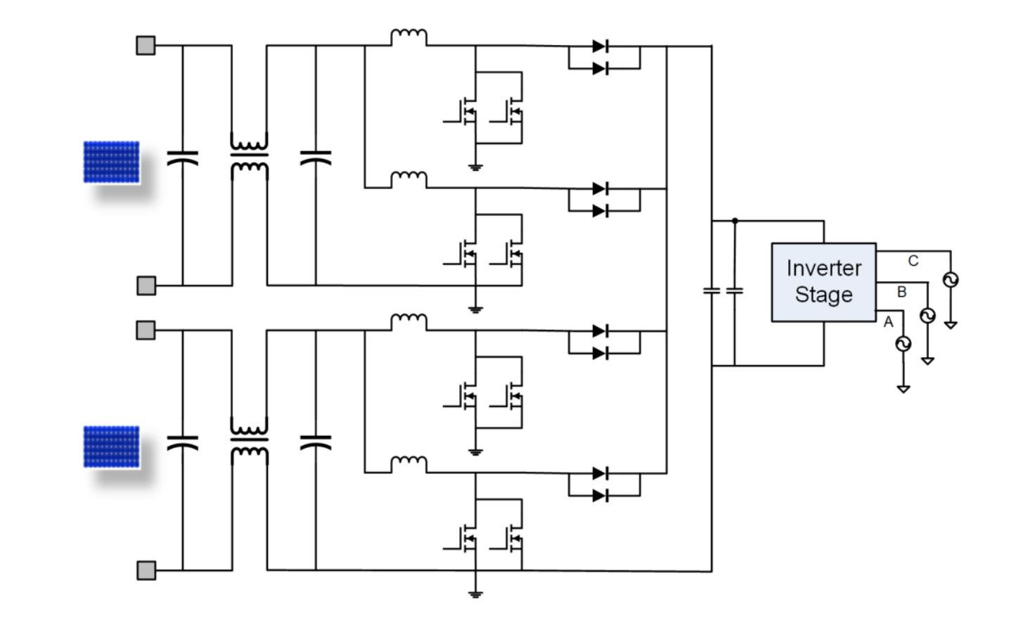
Another common option is powerful dc / dc boost converters, for example, network inverters for solar panels with MPPT, which are both the most expensive and most sought after, mainly used in power plants with power from 5 to 1500 kW. Such converters are built in 2 stages, where the 1st stage is a multiphase dc / dc boost (google as interleaved), which usually receives a constant voltage of 200 ... 600VDC at the input and increases it to a stable 800VDC. Further, an ordinary dc / ac inverter generates an alternating voltage. Such converters are built on the basis of DSP, and their structural diagram is as follows:
I hope you understand why this topology is important for developers of power electronics, as well as why it is important to learn how to develop boost converters with control based on DSP / MK. Now with clear motivation, we can proceed to the study of topology.
The boost boost converter is identical in principle to the buck buck converter because in both cases there are two stages of work. At the 1st stage, energy is accumulated in the inductor while the load is powered by the output capacitor. At the 2nd stage, energy is transferred from the inductor to the load and the output capacitor is simultaneously charged, which will provide energy to the load while the inductor is "recharged". Of course, in order to get a boost converter all the same, circuitry changes are needed, let's look at the circuit diagram of the boost converter:
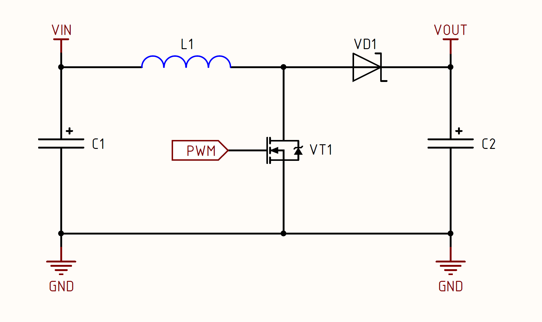
At first glance, it may seem to you that the topology is not like buck, but if you look closely, it will become clear that they are twins. Then you will see this more clearly, but for now, let's analyze the stages of the boost converter.
Further, these stages simply alternate and the converter works. For those who do not understand anything, I will explain how the voltage rises. At the moment when VT1 is closed, the throttle starts to discharge and at the moment of this “discharge” the voltage on it tends to infinity. Yes, this is in an ideal system, but in real life the voltage will be limited by the load resistance, which is connected in series with the inductor and diode, and also, if there is control, also feedback.
There is still to be supplemented by the stage of energy storage. At the moment of switching on, there is practically no stored energy in the output capacitor C2, but after the first stage of the discharge it is charged and the potential on it is equal to V out, which means that in the subsequent stages of energy storage, this capacity C2 will provide the load with energy, as a result, there will be no interruption in energy production for the load. From this it follows that C2 must have such a capacity that the stored energy is sufficient to provide power to the load for the duration of the opening of the transistor (t on ). In accordance with the above described, starting from the 2nd round of repeating stages, the stage of charge accumulation looks like this:

As you can see, two closed circuits are obtained. The "red" circuit closes through VT1 and the throttle is charged, and the "green" circuit closes through the load. The “mixing” of processes / energy in this case does not occur due to the presence of the diode VD1, because at any time, the potential at the cathode VD1 will be higher than the potential at the anode.
Now let's figure out what is happening with the voltage, what connection the output voltage has with the voltage at the input of the converter. As in the case of the buck converter, our boost has a linear dependence of the output voltage on the input, and the transmission coefficient is equal to the duty ratio:

As you can see, the relationship is simple and clear, accordingly, the output voltage can be adjusted simply by changing the duty cycle of our PWM signal. From the regulation formula, the algorithm also follows:
Now we understand how the boost converter works and the logic for controlling the output voltage. To consolidate the knowledge, we will analyze a couple of experiments on an oscilloscope and see these dependencies in practice.
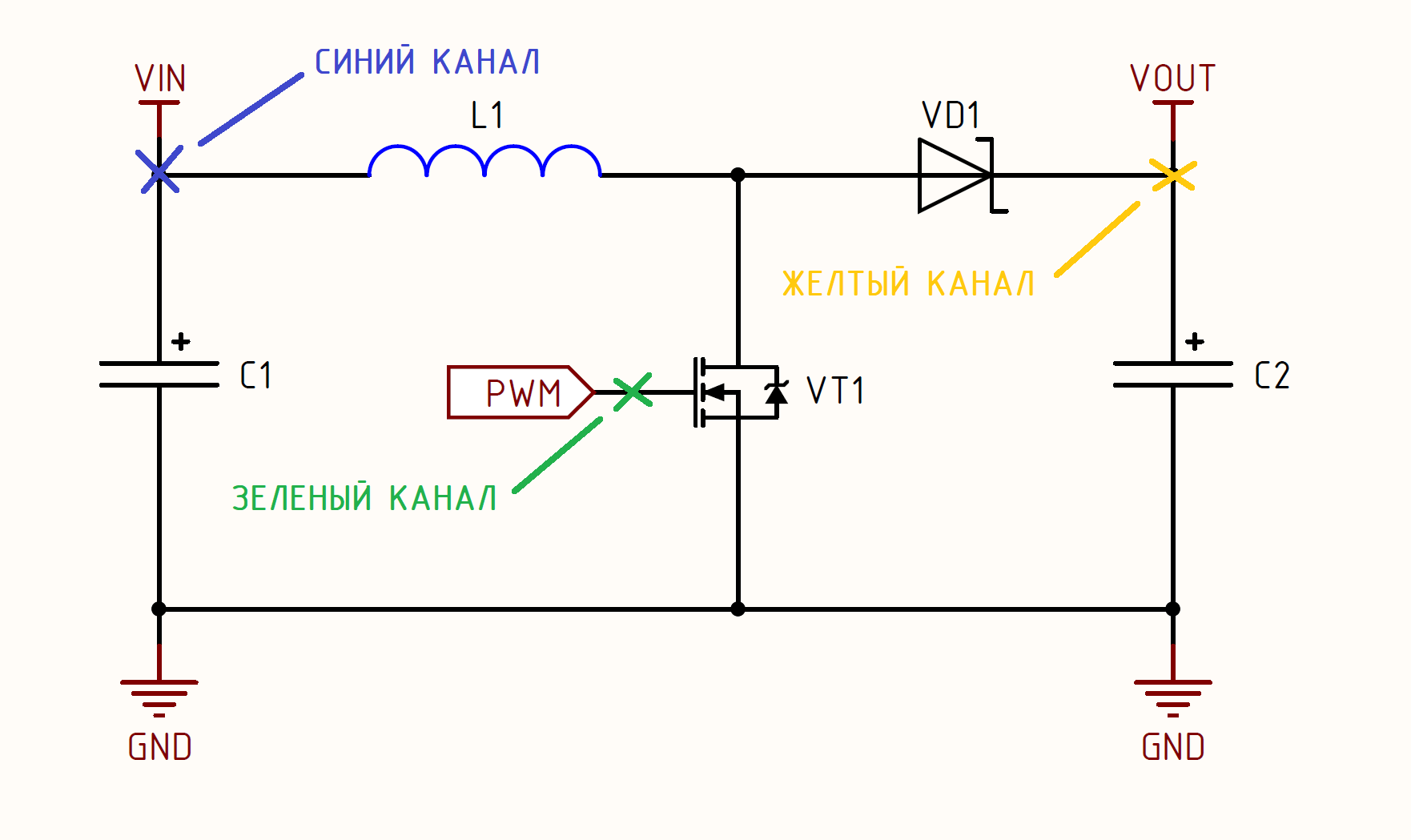
Let’s take a stabilized 10V voltage source, for example, a laboratory power supply, for illustration purposes, and apply a PWM signal to the VT1 transistor, the duty cycle of which will be changed during the experiment. Oscilloscope probes are connected to the following points in the circuit:
Now we have seen in practice that the output voltage linearly depends on the duty cycle, and therefore we can build a control system (CS) that will monitor the output voltage using the ADC and, depending on the measured value, reduce or increase it (duty).
As you understand, an ideal topology does not exist, otherwise there would not be so many of them and everyone would use only it, for example, a full bridge. In this case, boost converters also have a number of features that impose restrictions on the use of this topology:
From the above, I think it is quite obvious that it is reasonable to use a step-up converter when it is necessary to increase the voltage by a maximum of 3 ... 4 times and at the same time do not need galvanic isolation, in other cases it is already necessary to look in the direction of push-pull or full bridge topologies. The power for boost converters, in principle, does not have an upper limit, there are PFCs of tens of kilowatts and inverters for solar power plants per megawatt, which are built on this topology.
It's time to calculate the main power elements for the assembly of the prototype. As a power source, I will use a laboratory power supply with a 12V output, as if someone wants to repeat, but there is no LBP, then you can use the usual Chinese Mean Well on 12V 5A. An incandescent lamp at 36V and a power of 60 watts will act as a visual load today. I specifically selected the source and load so that the layout could be assembled in any village, while being cheap and withstanding a 1: 3 ratio. Total we have the following input data:
I'll start with the most interesting and important, because It is with the calculation of power inductance that developers usually have problems. I note right away that I will calculate the inductance value for the continuous current mode (CCM).
To begin, let's find the maximum value of the duty cycle at which our converter will work. This value will be set by the PWM controller with a minimum input voltage. For example, I plan to power the converter from a stabilized power supply, then V min = V nom. If you choose, for example, a lead-acid battery, then the voltage range is 10.2 ... 14.2V, and in this case, you need to take the value 10.2V for calculations, because it will achieve the maximum duty cycle. For a minimum I will take a value equal to 12V . The formula itself for the calculation is simple and looks as follows:

Now we need to calculate the ripple current in the inductor. Whoever read my article about buck converter probably remembered that we choose this value ourselves and usually it is laid down from 20 to 50%, but I will accept a 30% span and now we will find the current value itself:

Now we will calculate the minimum value of inductance that will be required to stay in continuous current mode:

For the manufacture of the throttle I will take the R26 / 14/11 throttle (R is the ring, and the numbers are the dimensions) from Kool Mu material with a permeability of 60, you can download the documentation for it and buy here - Lepkos .

Now let's find out how many turns we need to get this minimum inductance:

This is the minimum number of turns at which the converter will remain in continuous current mode with a minimum input voltage of 12V. For reliability, let's throw a few more turnsso that we will surely wind 3 more turns, that is, 29 turns . Let's find out what inductance we end up with with so many turns:

We got a new (final) value of the inductance and the number of turns, let's check if we have crossed the induction limit for this core:

The core is made of Kool Mu material for which the induction limit is 0.5 T. As you can see with this core, a five-fold margin is obtained.N - reliability! From this we can make an indirect conclusion that at a frequency of 100 kHz, about 300 watts can be pumped through this core.
Now let's decide on a winding wire. I have a lot of my favorite wire with a diameter of 0.6 mm in my warehouse, which corresponds to the cross section of one core of 0.283 mm 2 . The average current in the core will be about 5A, respectively, if wound in one core, then we get a current density of 5A / 0.283 mm 2 =17.66 A / mm 2 , which is a bit much and there will be excessive heating of the throttle. There are many places for winding, the core is large, so I will wind it in 2 cores , which will reduce the current density by 2 times to a value of 8.83 A / mm 2 . This will get overheated relative to the environment within 20 of S.
All throttle parameters determined: size R26 / 14/11, the material Kool Mu, the number of turns 29, the winding wire of 0.6 mm diameter and a winding core 2.
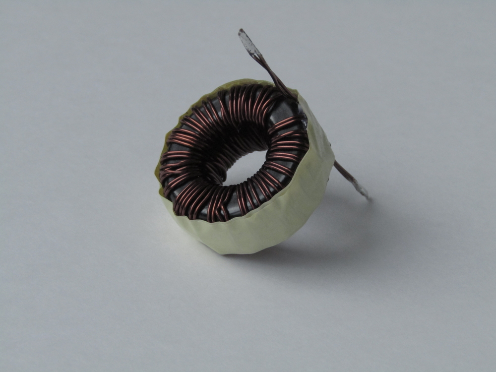
We went to wind it: We wound it, secured the end of the winding, we fixed the whole winding with tape - that's it. It remains to measure the actual value of the inductance of the inductor:
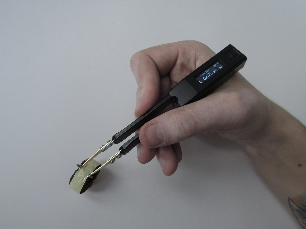
Got the required value! Now you can safely proceed to the calculation of the output capacity. The logic is basically simple - the larger the output capacity, the lower the ripple. True, it is worthwhile to understand that if you take the capacitance several orders of magnitude larger than the calculated one, the time constant will be too large and the control system (SU) will not work correctly, therefore, we calculate the minimum capacitance value for the capacitor (C2):

At frequencies within 200 kHz, where else cheap electrolytes are placed, I usually multiply this minimum value by 2 ... 3 and set this value. In the current task, I use a debugging power module, and electrolytes are already installed on it, which play the role of the output capacitance in the boost topology, which I will discuss in more detail in the next chapter.
The total capacity of electrolytes is 3000 μF, which is a lot in this task, because the board was designed for higher power. With such a large output capacitance, feedback is not sweet, but for experiments it will.
It remains to be said fluently about transistors. It is about transistors! I use a half-bridge module, and therefore implement a synchronous boost converter. The modules are equipped with IPP083N10N5AKSA1 transistors with a drain-source voltage of 100V, which gives an almost three-fold supply of voltage and therefore covers the task - we pass through the transistor VT1, and the diode VD1 is replaced by a similar transistor and, accordingly, we also pass.
Since I will talk about control algorithms in a separate article, today the converter will be controlled by the same program that was used in the article, which talked about buck topology, you can read here . In the code chapter, you can read in detail about the initialization of HRPWM and ADCs, as well as about their synchronization.
Changes in the code occurred in only one place, namely in the interrupt handler with the ADC - the cutoff threshold changed, because I used a different voltage divider. Well, I corrected the condition so that there is no excessive overshoot:
You will find the source project for TrueSTUDIO at the end of the article as an archive. Now that the principle of operation of the converter has been disassembled, all components have been counted, there is a control program, you can start assembling the layout and test it for operability and the correctness of the results.
We proceed to the most interesting and colorful stage, namely the assembly of the layout and verification of performance. At the beginning of the article, I mentioned the relationship between buck and boost topologies, let's now analyze this, because on the half-bridge module, this is extremely clear. First, let's look at the buck converter circuit: The
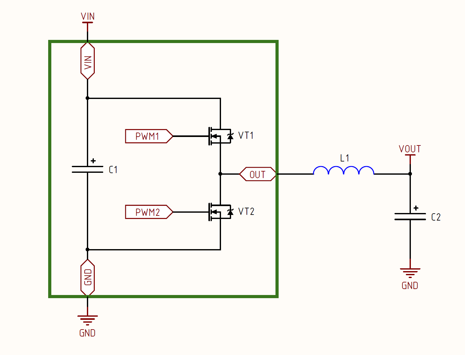
green frame highlights the components that are installed on the power module of the half-bridge , as you can see here C1 acts as an input capacitance, and capacitor C2 as an output capacitor. Now let's draw a boost converter circuit:

Who is attentive and noticed what has changed? Yes, in principle, nothing has changed, oddly enough, the only difference is that the input and output have changed places. As you can see, the topologies themselves are identical, and another interesting property follows from this - if a synchronous topology is applied, then the converter can work as a bidirectional converter!
Example? Easy! Imagine a portable device with a USB and Li-ion battery. When USB is connected, the converter operates in buck mode and charges the battery, as soon as the USB cable is disconnected, the converter goes into boost mode and lifts it from 5V to 5V from which the device is powered. Cool! And there are a lot of similar tasks where this feature is useful.
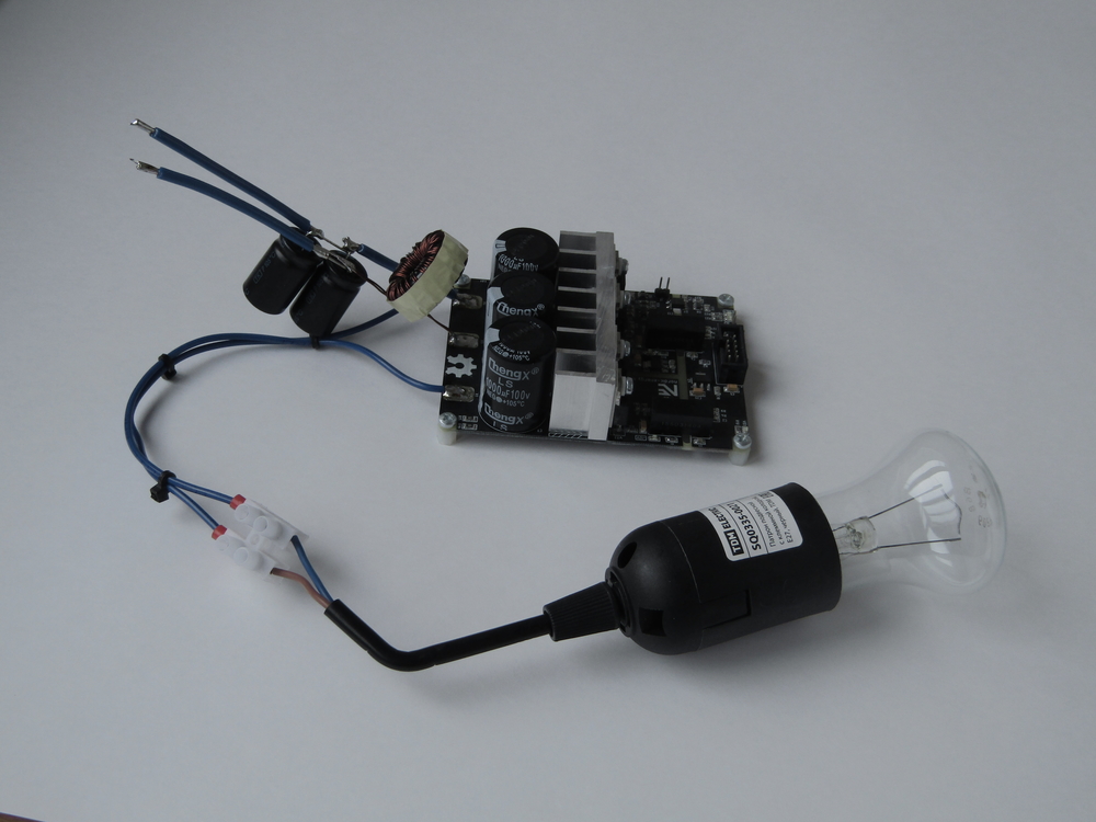
I assembled the layout according to the second scheme, and in it the capacitor C1 is just the output capacitance, that is, it is already installed and it is enough to throw a choke on the module, which we made and the input capacitance. In the role of the input capacitance C2, I used a pair of electrolytic capacitors at 4700 μF 25V and as a result we got such a model of the power section:
Now we connect the control module and the power source to the power section, in this case the laboratory power supply:
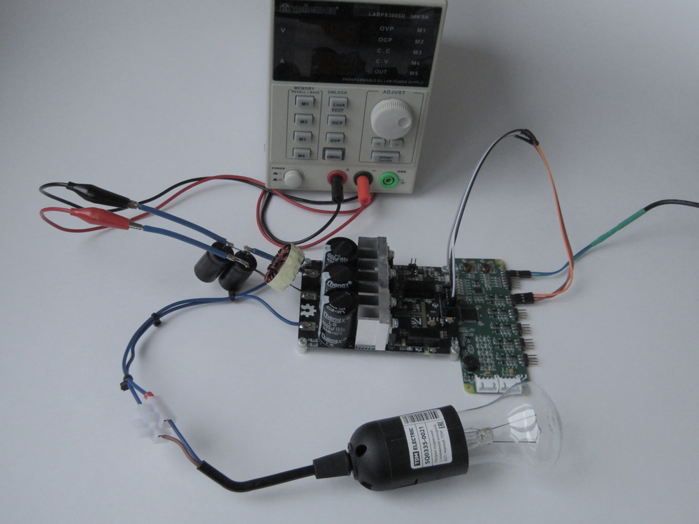
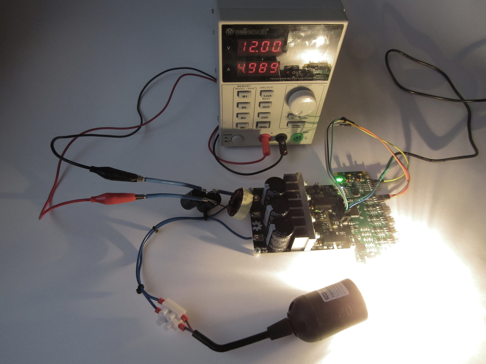
Now fill the firmware into the microcontroller, apply power from a laboratory technician, we will establish a duty cycle of 30,000 out of 45,000, which according to our formula will increase the input voltage by 3 times: V out = 12V / (1 - 0.66) = 12 / 0.33 = 36.36V. After that, we see that the lamp lights up brightly:

Now we connect the oscilloscope to the same points and see the following result:
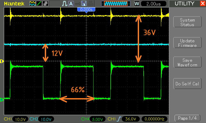
As you can see, the device works correctly: the voltage really increased 3 times, the input consumption is about 60 watts ( yes, I am aware that the lamp needs 36V “change” ), the lamp itself consumes current 1.61 A. For clarity, I will leave a short video in work:
It remains to find out how much the converter heats up under these conditions. I suggested that overheating would be minimal, as everything was calculated correctly, and the components were taken with a margin, so he placed the transducer in the environment with a temperature of about + 10 o C in order to enhance the contrast of the temperature field.
The methodology for testing is simple and consists of three stages:
After this experiment, it will be possible to draw approximate conclusions about the possibility of operating the converter in continuous operation, as well as to understand how the device overheats with respect to the ambient temperature, which will make it possible to predict the behavior of the device at higher ambient temperatures. And so let's get started:
Let's summarize ... The temperature of the transistors is normal, which means that the losses are miserable and the power module itself works correctly, there are no through currents, there are no problems with the installation of transistors, by the way, they are sitting on a ceramic substrate in a drop of MX-4 thermal paste, you don’t need to add a lot of paste - will be worse.
The temperature of the inductor is also normal, which means that the inductance is calculated correctly and the core dimensions are also used suitableyes, with a 5-fold margin :)) , that is, it does not saturate and the winding does not overheat with the current value of current density.
Today I examined the next topology of converters, I hope the material will become a useful cheat sheet for you when developing both conventional and DSP-controlled boost converters. Next time I plan to talk about the equally popular, and perhaps most useful, topology of a full bridge or full bridge, I will talk about the calculations of the transformer and how to make it.
For support in creating the material for the article, I would traditionally like to thank the company PCBway , which facilitates the process of creating layouts for me with my boards and stencils.

And most importantly - the source code of the power module, control board and the code itself, as usual, are available for all to see. So far, only in the form of archives, how do you get your hands, you finally need to make a repository on github.

Introduction
In the beginning, I would like to note one important point - although the article says that the control is carried out using a microcontroller, this does not mean that the calculation of the power part will be somewhat different from the calculation of a converter with an analog PWM controller. That is, you can safely apply the calculation procedure from this article when calculating the power unit for any boost conveter.
In the real world, there are many tasks that cannot be solved using standard analog PWM controllers. My favorite example is a voltage converter with MPPT algorithm. As soon as our task goes beyond the scope of the “standard” one and some additional control algorithm or logic of work appears, a situation arises in which the use of DSP simplifies the solution of the problem and at the same time reduces the cost of it, and most importantly allows it to be solved in principle.
It is worth a little talk about the tasks where you will meet the topology boost. The topology itself is known to many and many probably already implemented it when you had to get 5V from 1 cell of a li-ion battery, for example - you used a low-power dc / dc boost converter. Such low-power converters are often used in digital electronics, IoT, automation, self-powered devices and other tasks.
The second is not entirely obvious, but extremely important, application - PFC or power factor corrector. Most PFCs are the most common boost converter, which works according to a special algorithm, but in the end it rectifies and raises the input 85 ... 265VAC to + 400VDC. In the future, we will additionally consider this as an example.
Another common option is powerful dc / dc boost converters, for example, network inverters for solar panels with MPPT, which are both the most expensive and most sought after, mainly used in power plants with power from 5 to 1500 kW. Such converters are built in 2 stages, where the 1st stage is a multiphase dc / dc boost (google as interleaved), which usually receives a constant voltage of 200 ... 600VDC at the input and increases it to a stable 800VDC. Further, an ordinary dc / ac inverter generates an alternating voltage. Such converters are built on the basis of DSP, and their structural diagram is as follows:

I hope you understand why this topology is important for developers of power electronics, as well as why it is important to learn how to develop boost converters with control based on DSP / MK. Now with clear motivation, we can proceed to the study of topology.
Chapter 1 - Principle of boost converter operation
The boost boost converter is identical in principle to the buck buck converter because in both cases there are two stages of work. At the 1st stage, energy is accumulated in the inductor while the load is powered by the output capacitor. At the 2nd stage, energy is transferred from the inductor to the load and the output capacitor is simultaneously charged, which will provide energy to the load while the inductor is "recharged". Of course, in order to get a boost converter all the same, circuitry changes are needed, let's look at the circuit diagram of the boost converter:

At first glance, it may seem to you that the topology is not like buck, but if you look closely, it will become clear that they are twins. Then you will see this more clearly, but for now, let's analyze the stages of the boost converter.
- Stage accumulation of charge. At the moment the converter is turned on, the output capacitance C2 is under the potential V in , since current flows through inductor L1 and diode VD1. The control device (PWM controller or DSP) begins to generate a PWM signal and feeds it to the gate of the transistor VT1. When the transistor VT1 is opened, it turns out that the circuit is closed, the inductance L1 is connected to the power source and begins to accumulate energy. Current through VD1 does not flow, because the potential at the cathode is higher (about V in ) than the potential at the anode (GND potential, about 0V).
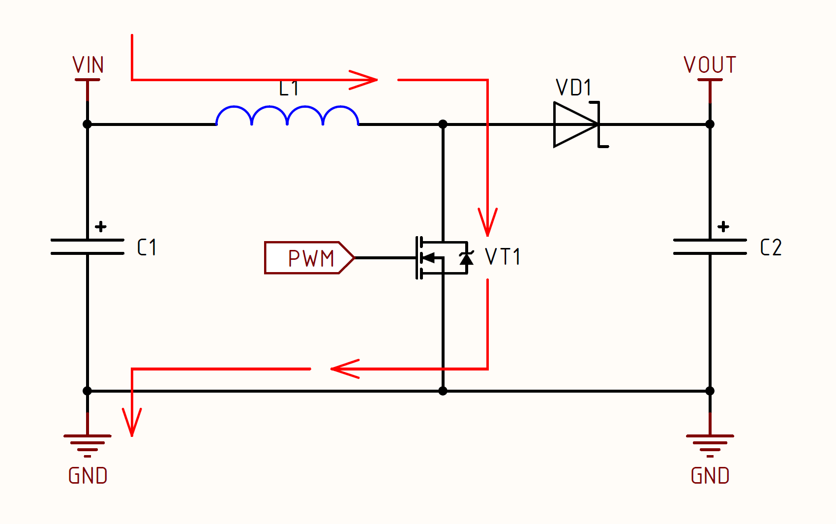
- Stage of inductance discharge. Now the PWM signal changes its value from 1 to 0 and the transistor VT1 closes. At this point, inductor L1 seeks to maintain the current value by increasing the potential. At the input of the inductor, the potential is still the same V in , and therefore the potential grows at the point "throttle-drain VT1-anode VD1". When the potential at this point becomes larger than the potential at the cathode VD1, the current begins to flow through VD1 to the load and simultaneously charge the output capacitance C2. At this stage, the circuit also closes, but not through VT1, but through the path “L1-VD1-C2-load”:
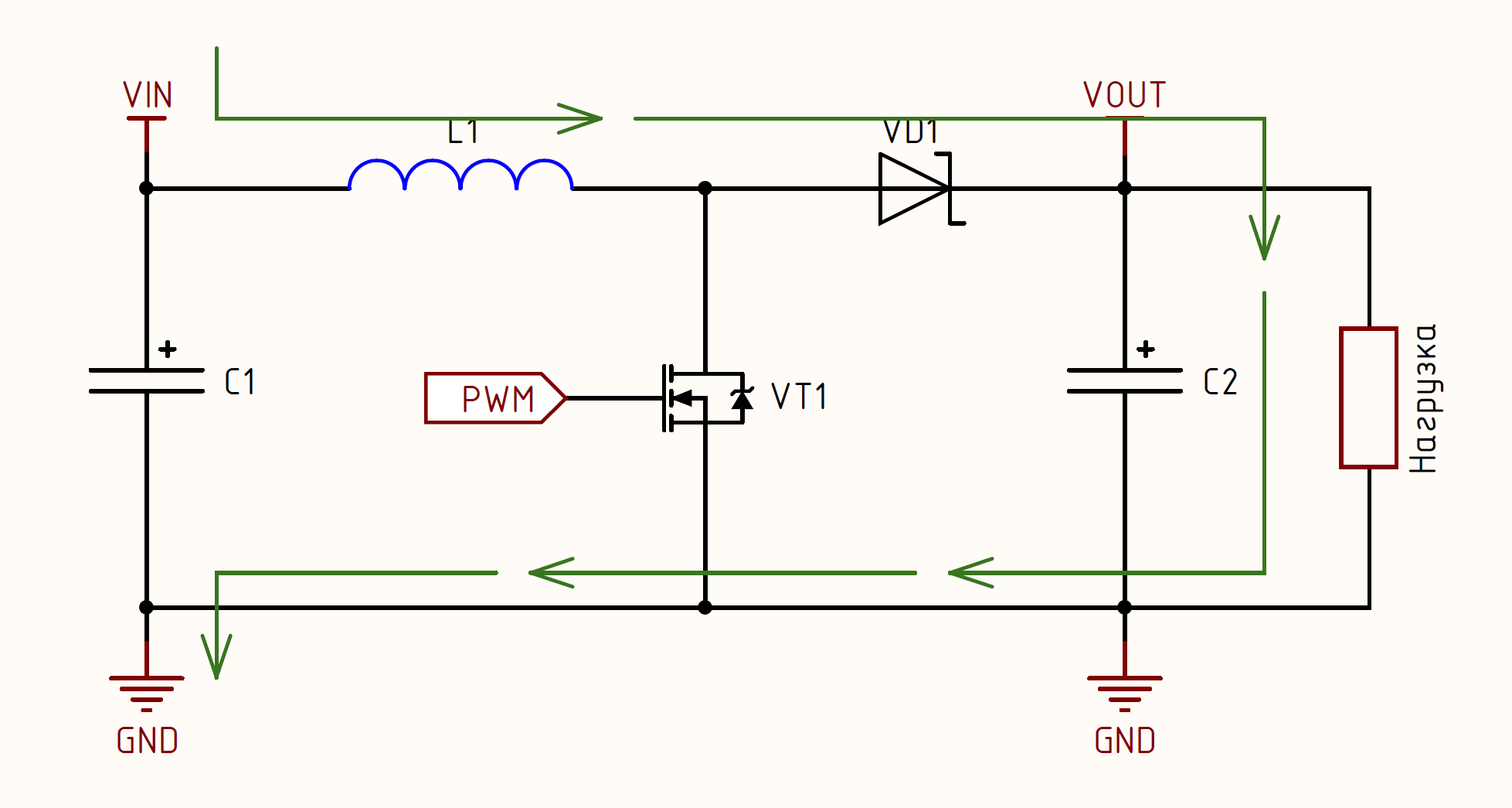
Further, these stages simply alternate and the converter works. For those who do not understand anything, I will explain how the voltage rises. At the moment when VT1 is closed, the throttle starts to discharge and at the moment of this “discharge” the voltage on it tends to infinity. Yes, this is in an ideal system, but in real life the voltage will be limited by the load resistance, which is connected in series with the inductor and diode, and also, if there is control, also feedback.
There is still to be supplemented by the stage of energy storage. At the moment of switching on, there is practically no stored energy in the output capacitor C2, but after the first stage of the discharge it is charged and the potential on it is equal to V out, which means that in the subsequent stages of energy storage, this capacity C2 will provide the load with energy, as a result, there will be no interruption in energy production for the load. From this it follows that C2 must have such a capacity that the stored energy is sufficient to provide power to the load for the duration of the opening of the transistor (t on ). In accordance with the above described, starting from the 2nd round of repeating stages, the stage of charge accumulation looks like this:

As you can see, two closed circuits are obtained. The "red" circuit closes through VT1 and the throttle is charged, and the "green" circuit closes through the load. The “mixing” of processes / energy in this case does not occur due to the presence of the diode VD1, because at any time, the potential at the cathode VD1 will be higher than the potential at the anode.
Now let's figure out what is happening with the voltage, what connection the output voltage has with the voltage at the input of the converter. As in the case of the buck converter, our boost has a linear dependence of the output voltage on the input, and the transmission coefficient is equal to the duty ratio:

As you can see, the relationship is simple and clear, accordingly, the output voltage can be adjusted simply by changing the duty cycle of our PWM signal. From the regulation formula, the algorithm also follows:
- To increase the voltage at the output - it is necessary to increase the duty cycle;
- To reduce the voltage at the output - it is necessary to reduce the duty cycle.
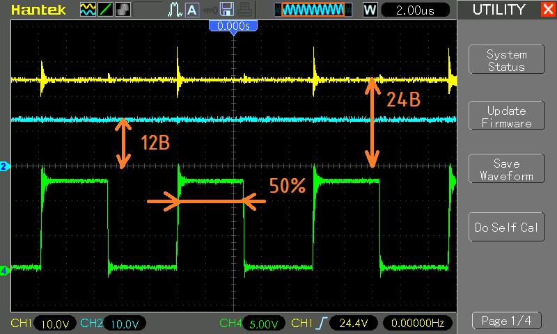
Now we understand how the boost converter works and the logic for controlling the output voltage. To consolidate the knowledge, we will analyze a couple of experiments on an oscilloscope and see these dependencies in practice.
Let’s take a stabilized 10V voltage source, for example, a laboratory power supply, for illustration purposes, and apply a PWM signal to the VT1 transistor, the duty cycle of which will be changed during the experiment. Oscilloscope probes are connected to the following points in the circuit:

- Experience No. 1. The input voltage (V in ) is 12V, the duty cycle of the PWM signal is 0.75:

- Experience No. 2. Input voltage (V in ) is 12V, PWM signal duty cycle is 0.5:
- Experience No. 3. The input voltage (V in ) is 12V, the duty cycle of the PWM signal is 0.25:

Now we have seen in practice that the output voltage linearly depends on the duty cycle, and therefore we can build a control system (CS) that will monitor the output voltage using the ADC and, depending on the measured value, reduce or increase it (duty).
Chapter 2 - Design limitations of boost converter
As you understand, an ideal topology does not exist, otherwise there would not be so many of them and everyone would use only it, for example, a full bridge. In this case, boost converters also have a number of features that impose restrictions on the use of this topology:
- The output voltage should not exceed the input more than 3 ... 4 times.
Experts will surely run up here and tell how they increased the voltage of the boost-ohm from + 5V by as much as + 180V using the MC34063 in an IN-12 watch! This is certainly wonderful, but let's estimate the duty cycle for this case, to raise the voltage from 5V to 180V, you need to make the converter work at a coefficient of about 0.972 (!). I think there is no need to tell that this is a bad idea, that at a high frequency the transients during switching transistors will have a comparable duration, and maybe even a longer one.
Also, with such a duty factor, it turns out that the transistor is almost always open, which means that current flows through it and we get the maximum possible value of static losses, and hence low efficiency.
What does this actually lead to ... at low power (the same case with mc34063), unstable operation, low reliability, current ripple and low efficiency combined with increased heating of power elements are guaranteed. At high power - broads.
For example, pay attention to PFC, they all work with a maximum ratio of 1: 4, namely the same universal input 85 ... 265VAC or a voltage regulator with their 90 ... 310VAC. As an example, you can consider network inverters with MPPT, where when the output is 800V, 200 ... 600VDC is fed to the input, that is, the ratio is 1: 4; - The voltage on the transistor. This limitation is closely related to the thesis about the ratio above and that’s why ... Transistor VT1 must have a drain-source voltage equal to the minimum output voltage, and in real devices also have a margin of at least 20% for ripple. High-voltage switches have a large channel resistance, and with a large ratio of voltage and input current will be very large, which will lead to large losses on the transistor;
- Diode voltage. If you carefully look at the converter circuit, it will become clear that a voltage equal to the output voltage is applied to the VD1 diode, that is, if you have a 400V output, then the diode must also withstand these 400V.
In this regard, this topology has an interesting plus, because Since the diode is high-voltage and the current flows in it several times lower than the current through the transistor, in many solutions the use of a Schottky diode or SiC diode will allow lower losses than the use of synchronous topology (half-bridge on transistors). This applies to solutions with an output of 200V or more, and the synchronous version of the topology is mainly relevant only up to a voltage of about 100V; - Capacitor voltage. It seems like an obvious point, but just in case, I’ll clarify - the output capacitor must withstand the voltage equal to the output, which in many tasks where boost is applied can be 400, 800, and even 1500VDC.
From the above, I think it is quite obvious that it is reasonable to use a step-up converter when it is necessary to increase the voltage by a maximum of 3 ... 4 times and at the same time do not need galvanic isolation, in other cases it is already necessary to look in the direction of push-pull or full bridge topologies. The power for boost converters, in principle, does not have an upper limit, there are PFCs of tens of kilowatts and inverters for solar power plants per megawatt, which are built on this topology.
Chapter 3 - Calculation of the power part of the Converter
It's time to calculate the main power elements for the assembly of the prototype. As a power source, I will use a laboratory power supply with a 12V output, as if someone wants to repeat, but there is no LBP, then you can use the usual Chinese Mean Well on 12V 5A. An incandescent lamp at 36V and a power of 60 watts will act as a visual load today. I specifically selected the source and load so that the layout could be assembled in any village, while being cheap and withstanding a 1: 3 ratio. Total we have the following input data:
- Input voltage: 12V
- Output voltage: 36 V
- Rated power: 60w
- Conversion Frequency: 100 kHz
Calculation and manufacture of a throttle
I'll start with the most interesting and important, because It is with the calculation of power inductance that developers usually have problems. I note right away that I will calculate the inductance value for the continuous current mode (CCM).
To begin, let's find the maximum value of the duty cycle at which our converter will work. This value will be set by the PWM controller with a minimum input voltage. For example, I plan to power the converter from a stabilized power supply, then V min = V nom. If you choose, for example, a lead-acid battery, then the voltage range is 10.2 ... 14.2V, and in this case, you need to take the value 10.2V for calculations, because it will achieve the maximum duty cycle. For a minimum I will take a value equal to 12V . The formula itself for the calculation is simple and looks as follows:

Now we need to calculate the ripple current in the inductor. Whoever read my article about buck converter probably remembered that we choose this value ourselves and usually it is laid down from 20 to 50%, but I will accept a 30% span and now we will find the current value itself:

Now we will calculate the minimum value of inductance that will be required to stay in continuous current mode:

For the manufacture of the throttle I will take the R26 / 14/11 throttle (R is the ring, and the numbers are the dimensions) from Kool Mu material with a permeability of 60, you can download the documentation for it and buy here - Lepkos .

Now let's find out how many turns we need to get this minimum inductance:

This is the minimum number of turns at which the converter will remain in continuous current mode with a minimum input voltage of 12V. For reliability, let's throw a few more turns

We got a new (final) value of the inductance and the number of turns, let's check if we have crossed the induction limit for this core:

The core is made of Kool Mu material for which the induction limit is 0.5 T. As you can see with this core, a five-fold margin is obtained.
Now let's decide on a winding wire. I have a lot of my favorite wire with a diameter of 0.6 mm in my warehouse, which corresponds to the cross section of one core of 0.283 mm 2 . The average current in the core will be about 5A, respectively, if wound in one core, then we get a current density of 5A / 0.283 mm 2 =17.66 A / mm 2 , which is a bit much and there will be excessive heating of the throttle. There are many places for winding, the core is large, so I will wind it in 2 cores , which will reduce the current density by 2 times to a value of 8.83 A / mm 2 . This will get overheated relative to the environment within 20 of S.
All throttle parameters determined: size R26 / 14/11, the material Kool Mu, the number of turns 29, the winding wire of 0.6 mm diameter and a winding core 2.

We went to wind it: We wound it, secured the end of the winding, we fixed the whole winding with tape - that's it. It remains to measure the actual value of the inductance of the inductor:

Got the required value! Now you can safely proceed to the calculation of the output capacity. The logic is basically simple - the larger the output capacity, the lower the ripple. True, it is worthwhile to understand that if you take the capacitance several orders of magnitude larger than the calculated one, the time constant will be too large and the control system (SU) will not work correctly, therefore, we calculate the minimum capacitance value for the capacitor (C2):

At frequencies within 200 kHz, where else cheap electrolytes are placed, I usually multiply this minimum value by 2 ... 3 and set this value. In the current task, I use a debugging power module, and electrolytes are already installed on it, which play the role of the output capacitance in the boost topology, which I will discuss in more detail in the next chapter.
The total capacity of electrolytes is 3000 μF, which is a lot in this task, because the board was designed for higher power. With such a large output capacitance, feedback is not sweet, but for experiments it will.
It remains to be said fluently about transistors. It is about transistors! I use a half-bridge module, and therefore implement a synchronous boost converter. The modules are equipped with IPP083N10N5AKSA1 transistors with a drain-source voltage of 100V, which gives an almost three-fold supply of voltage and therefore covers the task - we pass through the transistor VT1, and the diode VD1 is replaced by a similar transistor and, accordingly, we also pass.
Chapter 4 - Code for Drive Control
Since I will talk about control algorithms in a separate article, today the converter will be controlled by the same program that was used in the article, which talked about buck topology, you can read here . In the code chapter, you can read in detail about the initialization of HRPWM and ADCs, as well as about their synchronization.
Changes in the code occurred in only one place, namely in the interrupt handler with the ADC - the cutoff threshold changed, because I used a different voltage divider. Well, I corrected the condition so that there is no excessive overshoot:
void ADC1_2_IRQHandler (void) {
	ADC2->ISR |= ADC_ISR_EOC;
	adcResult = ADC2->DR;
	if (adcResult >= 3400) {
		dutyControl = dutyControl - 10;
	}
	else
	{
		dutyControl = dutyControl + 10;
	}
	SetDutyTimerA(dutyControl);
}
You will find the source project for TrueSTUDIO at the end of the article as an archive. Now that the principle of operation of the converter has been disassembled, all components have been counted, there is a control program, you can start assembling the layout and test it for operability and the correctness of the results.
Chapter 5 - Assembling the layout and testing the operation of the converter
We proceed to the most interesting and colorful stage, namely the assembly of the layout and verification of performance. At the beginning of the article, I mentioned the relationship between buck and boost topologies, let's now analyze this, because on the half-bridge module, this is extremely clear. First, let's look at the buck converter circuit: The

green frame highlights the components that are installed on the power module of the half-bridge , as you can see here C1 acts as an input capacitance, and capacitor C2 as an output capacitor. Now let's draw a boost converter circuit:

Who is attentive and noticed what has changed? Yes, in principle, nothing has changed, oddly enough, the only difference is that the input and output have changed places. As you can see, the topologies themselves are identical, and another interesting property follows from this - if a synchronous topology is applied, then the converter can work as a bidirectional converter!
Example? Easy! Imagine a portable device with a USB and Li-ion battery. When USB is connected, the converter operates in buck mode and charges the battery, as soon as the USB cable is disconnected, the converter goes into boost mode and lifts it from 5V to 5V from which the device is powered. Cool! And there are a lot of similar tasks where this feature is useful.
I assembled the layout according to the second scheme, and in it the capacitor C1 is just the output capacitance, that is, it is already installed and it is enough to throw a choke on the module, which we made and the input capacitance. In the role of the input capacitance C2, I used a pair of electrolytic capacitors at 4700 μF 25V and as a result we got such a model of the power section:

Now we connect the control module and the power source to the power section, in this case the laboratory power supply:

Now fill the firmware into the microcontroller, apply power from a laboratory technician, we will establish a duty cycle of 30,000 out of 45,000, which according to our formula will increase the input voltage by 3 times: V out = 12V / (1 - 0.66) = 12 / 0.33 = 36.36V. After that, we see that the lamp lights up brightly:

Now we connect the oscilloscope to the same points and see the following result:

As you can see, the device works correctly: the voltage really increased 3 times, the input consumption is about 60 watts ( yes, I am aware that the lamp needs 36V “change” ), the lamp itself consumes current 1.61 A. For clarity, I will leave a short video in work:
It remains to find out how much the converter heats up under these conditions. I suggested that overheating would be minimal, as everything was calculated correctly, and the components were taken with a margin, so he placed the transducer in the environment with a temperature of about + 10 o C in order to enhance the contrast of the temperature field.
The methodology for testing is simple and consists of three stages:
- I place the converter in an environment with a temperature of +10 o C and wait until it cools and becomes almost indistinguishable in the thermal imager against the general background;
- I turn on the converter, let it work for 5 minutes and measure the general view of the converter and separately the power components;
- I leave the converter to work for another 1 hour and measure it again, see how much the temperature of the components has risen.
After this experiment, it will be possible to draw approximate conclusions about the possibility of operating the converter in continuous operation, as well as to understand how the device overheats with respect to the ambient temperature, which will make it possible to predict the behavior of the device at higher ambient temperatures. And so let's get started:
- Измерение №1 — преобразователь поместили в окружающую среду с температурой около +10 oС:

Тут видно, что платы практически полностью слились с окружающей средой, а значит можно включать и приступать к оценке температур преобразователя уже под номинальной нагрузкой. - Измерение №2 — преобразователь работает на 100% номинальной нагрузке в течение 5 минут, температура окружающей среды около +10 oС:

После 5 минут работы картинка стала более контрастной и на ней отчетливо видно как сам преобразователь, так и основные нагревающиеся компоненты. Рекордсменами по перегреву стали изолированные dc/dc для драйверов транзисторов с температурой +29 oС, но тут ничего странного нет, т.к. температура перегрева +20...30 oС является для них номинальной о чем отражено в документации. Второе место занимается дроссель, температура которого составляет +28...29 oС, что более чем хорошо, т.к. часто рабочая дросселей вполне может достигать планки и в +80...100 oС. Температура радиатора составляет +20...21 oС, а транзисторы горячее всего на градус, а может и меньше, т.к. любой тепловизор на самом деле не самый точный на свете прибор. - Измерение №3 — преобразователь работает на 100% номинальной нагрузке в течение 1 часа, температура окружающей среды около +10 oС:

Через час работы температуры подросли и устаканились, пробовал еще измерять через 3 часа, но результат не изменился, вернее изменения на уровне погрешности измерения, поэтому эту стадию не стал добавлять. Пока же давайте посмотрим на температуры после выхода преобразователяна крейсерскую скоростьв номинальный режим.
Температура радиатора подросла на +4 oС, а транзисторы «слились» с ним, т.к. все прогрелось и тепловой поток равномерно распределился. Температура на изолированных dc/dc подросла на +9 oC and they reached the passport indicators of overheating, even the margin remained at a couple of degrees. The temperature of the throttle increased by +3 o C.
Let's summarize ... The temperature of the transistors is normal, which means that the losses are miserable and the power module itself works correctly, there are no through currents, there are no problems with the installation of transistors, by the way, they are sitting on a ceramic substrate in a drop of MX-4 thermal paste, you don’t need to add a lot of paste - will be worse.
The temperature of the inductor is also normal, which means that the inductance is calculated correctly and the core dimensions are also used suitable
Bonus inquisitive
Keep a light bulb in the thermal imager :))


Conclusion
Today I examined the next topology of converters, I hope the material will become a useful cheat sheet for you when developing both conventional and DSP-controlled boost converters. Next time I plan to talk about the equally popular, and perhaps most useful, topology of a full bridge or full bridge, I will talk about the calculations of the transformer and how to make it.
For support in creating the material for the article, I would traditionally like to thank the company PCBway , which facilitates the process of creating layouts for me with my boards and stencils.

And most importantly - the source code of the power module, control board and the code itself, as usual, are available for all to see. So far, only in the form of archives, how do you get your hands, you finally need to make a repository on github.
