How we developed the Librem 5 devkit completely on free software
- Transfer
 From the translator: Librem 5 (on the render) - a protected smartphone for Linux from the company Purism, which is created on the most open hardware and software through crowdfunding .
 Today we will talk about the development of the Librem 5 Developer Kit and how we used only 100% free software in its development.
The design of the devkit is published under the terms of the GNU GPLv3 + license, the Git hardware repository is here .
KiCad is an obvious choice of EDA.
Before the start of development, it was not entirely clear which way to develop the project. In particular, which tool to choose for automation electronics design (EDA). Initially, the idea was to change the i.MX 6QP OpenRex board from FEDEVEL to meet all the requirements for devkit, but we immediately faced two main problems: they used an archaic i.MX 6QP processor, and even worse, the board was developed in a proprietary Altium system . Fortunately, I already had the experience of designing electronics using EDA KiCad, so we managed to create a devkit design using 100% free software.
KiCad is an obvious choice not only because of the free license (GNU GPLv3 +), but also because it is a very functional set for designing electronics, which even surpasses some expensive proprietary tools.
Selection of components that meet the requirements
The first step in devkit development is to find components that meet the requirements defined during the campaign. In addition to compliance with the stated specifications, when searching for components, we decided to add a few additional bells and whistles; including:
- charge controller (BQ25896)
- 18650 battery holder for optional lithium-ion battery
- USB-C
- mini-HDMI
- SD card controller and micro-SD connector (since i.MX 8M has only two uSDHC controllers)
- Ethernet / RJ45
- audio codec
- headphone speaker
- microphone
- 4-pin CTIA / AHJ 3.5 mm headphone jack (with a choice between built-in and external microphone)
- GPG smart card reader and connector
- vibration motor
- programmable LED
- volume and power buttons
- hardware switches and boot mode switch
- 16Mb SPI NOR flash memory
- real time clock (RTC)
As planned, we added through holes for UART debugging pins that are not occupied by default (serial over USB works on the default image that comes with the devkit). Hint: if you don’t like to solder, then heders support press fit, look for part number Autosplice 23-1063. The board has a SMD 2 × 5 JTAG support surface, and its functionality has been tested on a prototype; If you want to play around, then look for the part number GRPB052VWQS-RC.
For the WWAN / baseband modem and WiFi + BT it was clear that you need to find some ready-made modules, for example, with surface mount. At an early stage, Nicole had the brilliant idea of using the mPCIe and M.2 modules to make modular modules, with the possibility of an upgrade in the future. In the end, we stopped at the SIMCom SIM7100A / E mPCIe modem module and the M.2 RedPine RS9116 Wi-Fi + BT module.
Drawing start
At the conclusion of the research phase, we had to start implementing our ideas. The i.MX 8M Quad processor has just appeared on the market. To get a breakthrough in development, as well as add modularity and the possibility of future upgrades, we chose the system-on-module (SOM) option , which includes SoC, SDRAM, eMMC and PMIC. But even in the early stages of development, when we were just starting to draw diagrams, the serial production of some of the SOMs of interest to us had not yet begun. Around mid-April, we established a good relationship with EmCraft, which just started the first major SOM production cycle and was close to issuing a hardware architecture specification. We decided that the EmCraft SOM and their resources are exactly what we need. As soon as a specific SOM was chosen, we immediately proceeded to drawing diagrams.
The process of selecting specific components for devits was carried out simultaneously with the mapping. All work was carried out in the Git version control system.
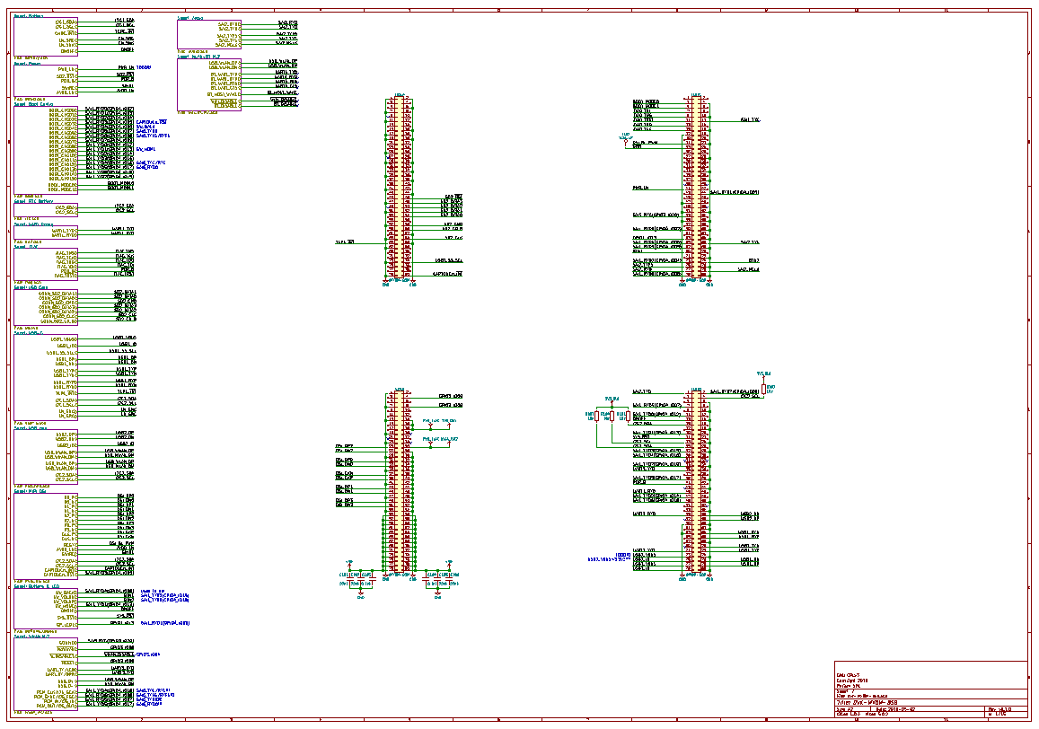
Fig. 1. Early edition of the scheme of May 2 (hash of git-commit 023915d5)
At the completion of the schemes we exported the netlist file , which brought us closer to bringing the devitch to life.
HP_DET simulation
In addition to KiCad, from free software, we also used a tool called Qucs-S and a SPICE-compatible Xyce emulation tool to emulate the headphone sensor chip, which includes a zener diode to protect the corresponding GPIO from too high or too low input voltage from the HP DAC output from audio codec. The combination of Qucs-S and Xyce made it possible to use in the chip the SPICE model of the MMSZ4688T1G diode , which best represents the physical state of the empty 3.5 mm jack with simultaneously active HP DAC.

Fig. 2. Simulation of the HP_DET scheme using Qucs-S and Xyce
This imitation, as well as the simple case of DC, where the internal 3.5 mm jack switch is open and 1MΩ only reaches the default voltage of 3V3_P - this made sure that a particular protection method really works.
Creating sites
Around the middle of June, we completed the compilation of a list of materials (BOM) , began to place orders for components and began to create the outlines of all the sites in the device (chips, connectors, modules, etc.). We took the recommended specifications from the documentation and checked four times that everything is correct.

Fig. 3. Platform of the charge controller BQ25896 (U301 on the dev-board, is under SOM)
In a magnificent mode of 3D viewing KiCad, we created three-dimensional outlines of almost all components.
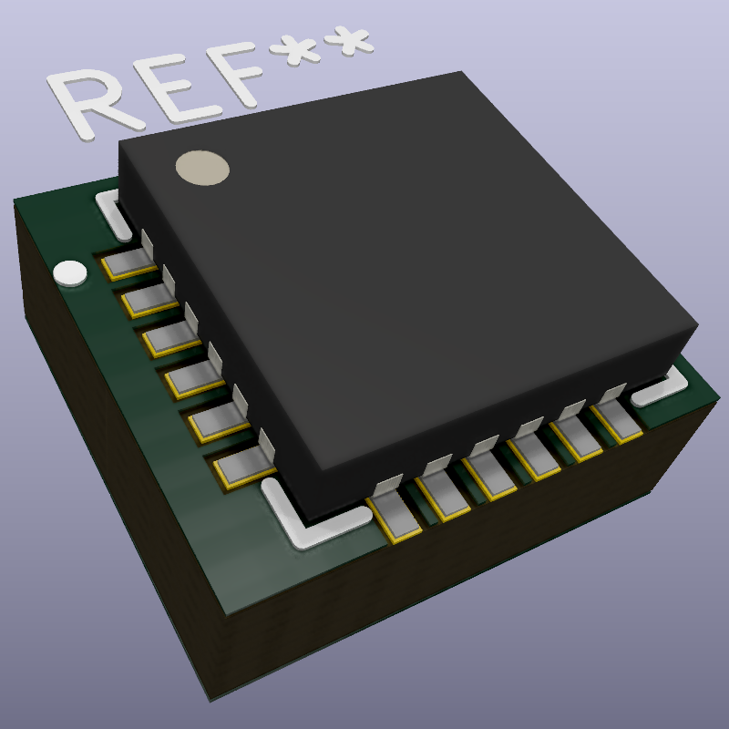
Fig. 4. 3D-model charge controller BQ25896
Level Planning, Layout and KiCad Update
At an early stage, a rough level plan was drawn up to quickly estimate what area of the integrated circuit would be used (90 × 180 mm) and where to place larger components (connectors, jacks, card slots, mPCIe and M.2 sockets, modules, and t d.) After placing on the layout, some of the details were still moving, but quickly consolidated on specific places.
At the end of June, we began to lay the layout, starting with USB-C (commit a1bfc689). This marked the beginning of the layout.
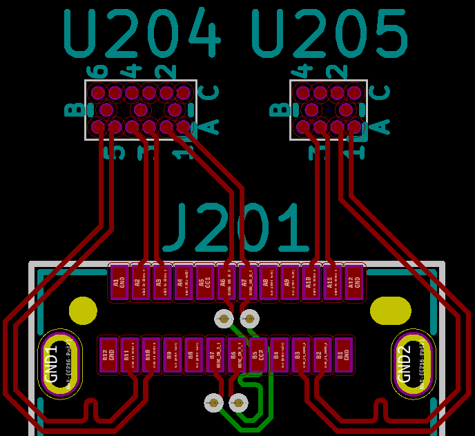
Fig. 5. The first commit to distributing

Fig. 6. What was the end result USB-C layout
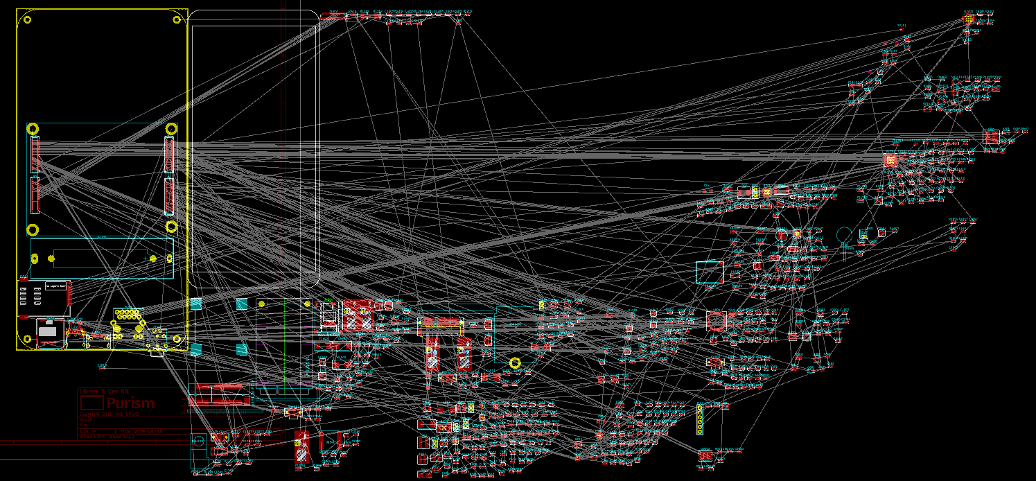
? 7. Early version of the scheme before placing components and wiring
The wiring process required a delicate balance between speed and checking that everything was done correctly without errors, including careful routing of resistance control tracks and sensitive analog lines.
Initially, there was no certainty how many layers are needed and whether components should be placed on both sides of the board. We knew that on the i.MX 8M board there are eight layers and components on both sides, but we were sure that we could reduce the number of layers. We quickly realized that the back side of the board would have to be placed components, because on the phone some modules are on the back side of the board (display side), including display connectors, proximity sensor / light sensor, programmable LED, speaker and microphone. The presence of components on both sides made the layout process somewhat easier, as it freed up a bit of space where you can place SPI NOR flash memory, card reader, RTC, 2.8V LDO, various ICs and other components. As for the number of layers, we decided to reduce it to six. Two additional layers decided to add only if we are stuck in a dead end and can’t pave any chains. Fortunately, this did not happen and the design with six layers remained.
We decided to use a common layout that provides the optimal balance between ease of wiring and reduces unintentional emissions. As a dielectric substrate, we took a laminate with a NP-180TL copper foil from NAN YA, which has a relative dielectric constant of about 4.11 at our average operating frequency of about 1.7 GHz. Our RF power line calculations for microstrip and coplanar waveguide power lines of the board (CPW) using this layout can be found in the Git repository.

Fig. 8: DevKit Layer Layout
Before the implementation of devikit in KiCad, we did not know whether to release alpha versions or stick to the classic more stable releases like 4.0.7. Although the “nightly builds” have a few useful features, we still decided to stick with stable releases, so that we don’t have to frequently update KiCad and risk the emergence of several simultaneous versions.
When we started, KiCad version 5.0.0 was released! On July 16, we upgraded the project to KiCad 5.0.0 without any problems (in particular, commits 4f70b865 and a4e3de8a). Fortunately, this update coincided with the transition of most of our passive components from 0603 to 0402, since the new sites in KiCad are slightly different from the old default values, and the rounded corners of the sites are more effective for lead-free solder.
After updating to 5.0.0, we focused on prototyping - and within a month (namely, on August 14, with a commit 9b4dd2e0), the number of undissolved chains was reduced to zero.

Fig. 9: Release candidate of August 14 with a commit 9b4dd2e0 fixed a zero number of undiluted chains.
After completing the routing and design rules check (DRC), we arranged the layout for a week.
When prototyping the board, the most useful resources were the reference book on prototyping integrated circuits from official documentation and the Toradex prototyping guide .
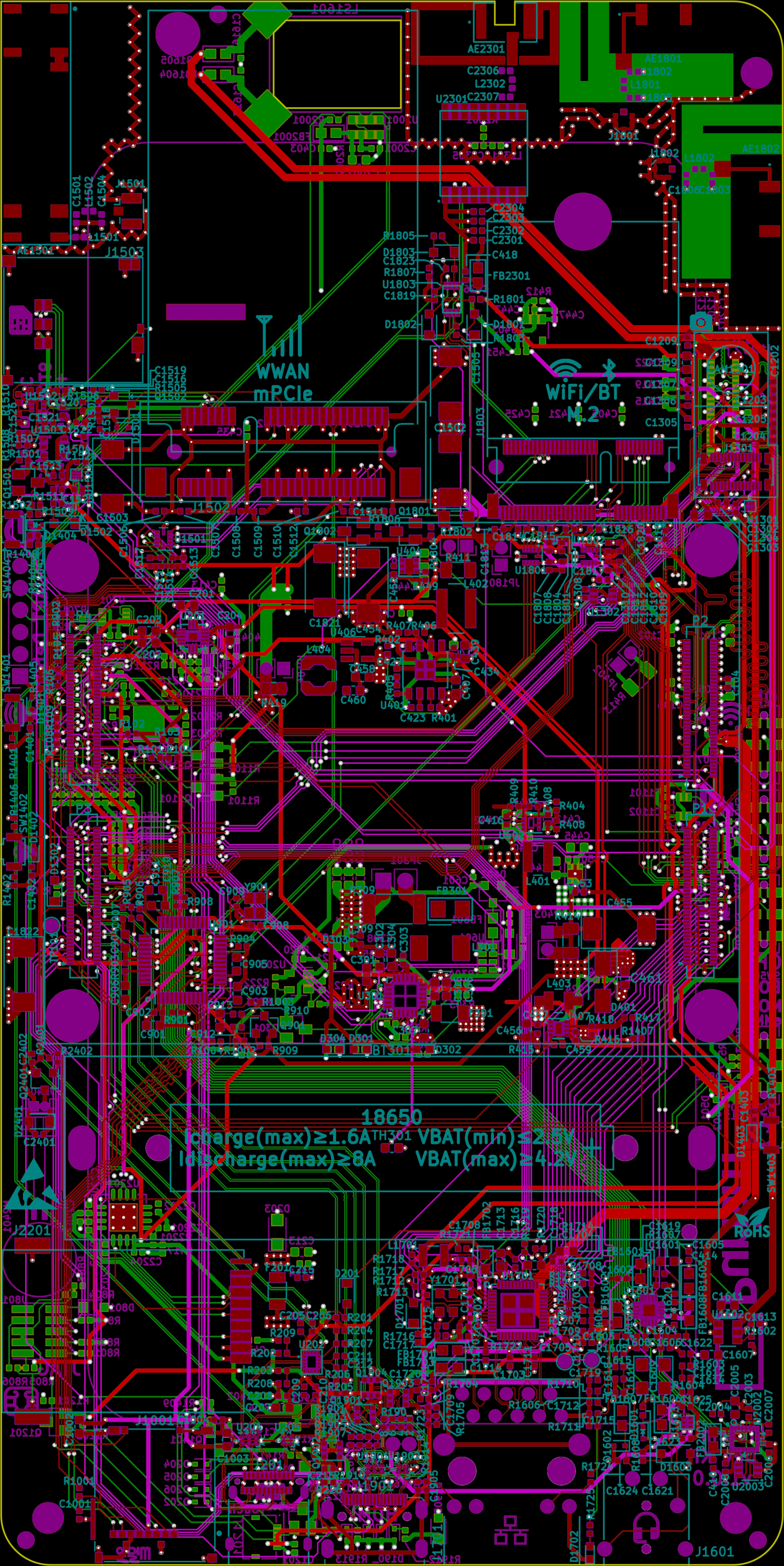
Fig. 10. Final layout (copper coated areas are hidden)
Exporting files and sending to production
After the layout was complete, it was necessary to export all the files necessary for the production and assembly of the boards. Exporting Gerber files to KiCad is fairly straightforward. However, the contractor requested another layout and layout for the assembly, which required some effort.
We usually used Gerbv from gEDA to preview the files on export. This is what our devkit in Gerblook looks like - this tool uses Gerbv and ImageMagick for web rendering.
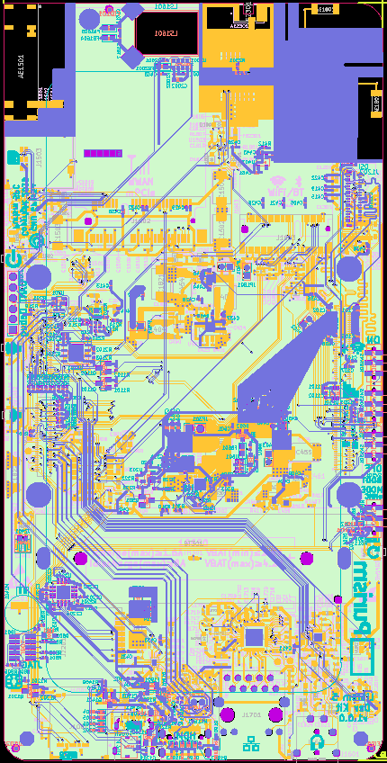
Fig. 11. Gerber devkit files when browsing in Gerbv
To create a drawing of the required type, we used the layers F.Fab / B.Fab. They display the locations, contours, polarity, and reference designations of all components on the board. Using the F / B.Fab layers for each site, we were able to create the final drawing by printing out F.Fab and B.Fab into separate PDF files, and then merging them into one document.

Fig. 12. Scheme by SOM
Even more had to work on the scheme for production. To do this, you had to export notes from the Cmts.User layer along with the board outline as one DXF archive, and then export all the marks for drilling holes as another DXF archive. After creating these two files, they are combined in the footprint drawing. Having received this special “footprint”, which combines two DXF files, we hide almost everything in the layout - and import this special footprint “for the plant” (without saving the temporary layout). At the moment everything you need is on the Dwgs.User layer; therefore, you can print it together with the frame into the final PDF for production.

Fig. 13. Marks for drilling holes
Together with all these files and documents, the IPC-D-356 netlist is used, with which the plant can carry out a test using the “flying probe” method and verify that there is no short circuit or an open circuit. We also prepared a CSV file (so that the factory knew where to place and how to orient all the components), and finally, a manually edited GenCAD file (for programming a factory soldering robot).
Prototype testing
We sent the final files for production, answered all the contractor’s questions and changed everything they asked. The files were sent around the end of August - and we waited impatiently for our design to hit the assembly line in Shenzhen. Unfortunately, as we told in the blog , significant delays in the production of prototypes occurred due to unforeseen circumstances, such as severe weather and Golden Week [a national holiday in China - approx. trans.]. Because of these delays, we decided to order the production of prototypes at a domestic plant that delivered us the boards two weeks faster than the Chinese.

Fig. 14. The prototype of the devkit panel v0.1.2 (before assembly)
After building a small batch of prototypes, they were quickly sent to our engineers for debugging and software development. Fortunately, due to public discussion and a comprehensive analysis of the design, there were very few errors in the hardware (three relatively minor adjustments to the layout / list of circuits and one mechanical correction). Over the next two months, prototypes were used to polish the software.
Final production and supply
Around early-mid-November, after making minor adjustments to the design and testing of almost all hardware subsystems, we conducted a re-export procedure and re-released the files for production and final assembly. Some of our employees spent December 10-22, helping to assemble, test, pack, and send devits to our bakers (many delivered before Christmas!)
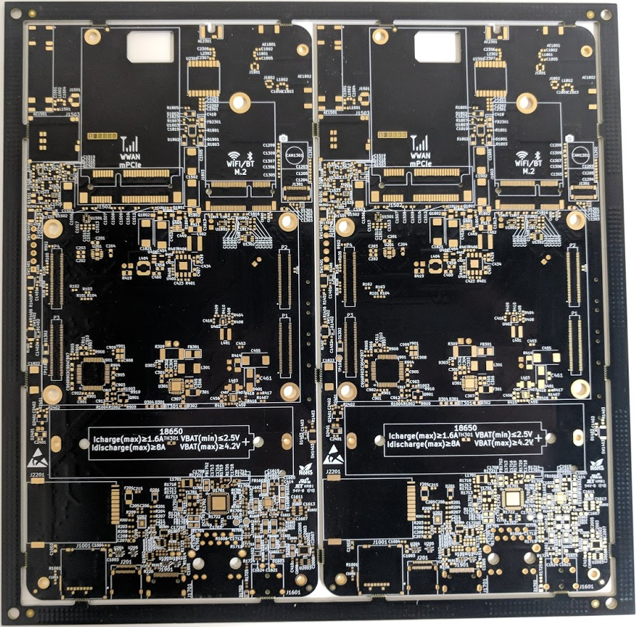
Pic. 15. The final view of the v1.0.0 devkit panel (before assembly)
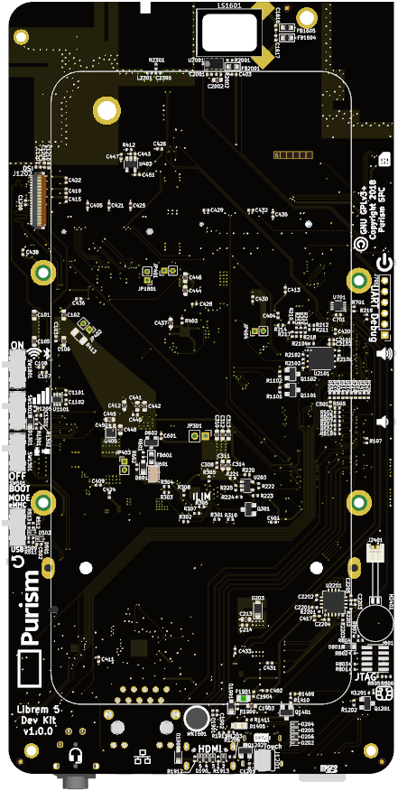

. Figure 16. Fully assembled device compared to 3D model (display side)


. 17. Fully assembled device compared to 3D model (SOM side)
The whole process required a lot of effort, but it was worth it. Especially when we saw how fruitfully the community can use the results of our work. Some have already begun to develop 3D printed enclosures for a devkit. I can't wait to see what cool software and what use cases you will come up with for these amazing cards! Feel free to report all the cool stuff by email to
feedback@puri.sm. If this is really great, we will talk about your development in future blog posts. Now we have all the time it takes to send out Librem 5 phones. So until next time, do not lose resource!